具有輕掺雜汲極之複晶矽薄膜電晶體電性模型建立
70
0
0
全文
(2) 具有輕掺雜汲極之複晶矽薄膜電晶體電性模型建立 The I-V Model of Poly-Si TFTs with LDD Structure 研 究 生:高士欽 指導教授:冉曉雯. Student: Shih-Chin Kao 教授. Advisor: Dr. Hsiao Wen Zan 國立交通大學. 光電工程所碩士班 碩士論文 A Thesis Submitted to Institute of Electro-Optical Engineering College of Electrical Engineering and Computer Science National Chiao Tung University in partial Fulfillment of the Requirements for the Degree of Master in Electro-Optical Engineering June 2005 Hsinchu, Taiwan, Republic of China. 中華民國九十四年六月.
(3) 具有輕掺雜汲極之複晶矽薄膜電晶體電性模型建立 研究生:高 士 欽 . 指導教授:冉 曉 雯 教授. 國立交通大學 光電工程研究所碩士班 中文摘要 複晶矽薄膜電晶體在面板技術的應用上,由於其具有高遷移率,可以實現系 統面板(System on Panel)的技術,也就是可以將周邊電路直接以複晶矽薄膜電晶 體實現在玻璃基板上,與面板矩陣電路結合成所謂的系統面板。然而,在這樣的 技術發展中,準確的元件模型是SPICE tool中最重要的基礎,在本論文中,我們 特別針對具有輕摻雜汲極(Lightly-Doped Drain, LDD)結構之N型低溫複晶矽薄膜 電晶體建立DC電性模型。 首先,我們研究輕摻雜汲極寄生電阻的萃取方法。利用變化不同的通道長度 和不同的輕摻雜汲極長度,可以萃取出不同的寄生電阻。然後我們建立包含寄生 電阻效應的元件等效電路,根據等效電路,推導出元件的電性模型。模型產生的 電性,可以準確描述元件在通道長度6 µm - 30 µm以及LDD長度0 µm - 3 µm 的輸出特性。除了基本的電流輸出特性,我們也分析元件的轉導特性以及輸出阻 抗特性在不同偏壓下的變化,並利用前述的模型解釋寄生阻抗所造成的影響;另 外,由於複晶矽薄膜特有的DIGBL(Drain-Induced Grain Barrier Lowering)效應, LDD區域的阻抗效應其實會在LDD長度越長通道長度越短的狀況下影響到元件 的線性區特性,我們也針對LDD結構在不同偏壓下的等效阻抗變化做了初步的模 型;最後,我們並結合了元件在變溫量測下定義出的晶粒邊界位障,成功建立了 包含薄膜差異性、元件LDD結構差異對元件特性影響的模型。. I.
(4) The I-V Model of Poly-Si TFTs with LDD Structure Student: Shih-Chin Kao. Advisor: Dr. Hsiao Wen Zan. Institute of Electro-Optical Engineering National Chiao Tung University Abstract. To realize the system-on-panel (SOP) technology, in which we combine the peripheral circuit and panel array circuit on the same glass substrate, it is essential to develop accurate device I-V model for Poly-Si TFTs. In this thesis, we especially focus on the modeling of n-channel devices with LDD(Lightly-Doped Drain) structure. Firstly, parasitic resistance parameters were extracted from devices with various channel length and LDD length. Then, the device equivalent circuit had been developed including the extracted parasitic resistance parameters. An accurate I-V model was established by combining basic TFT model and the parasitic resistance effects. The model had been verified for devices with channel length varied from 6. µm to 30 µm. The transconductance and output resistance behavior are also well explained by our proposed model. The special DIGBL effect of poly-Si film is also observed when the devices with large LDD length and short channel length. We used testkey structure to clarify this effect and established adequate model to explain this phenomena. Finally, the model was combined with the grain barrier height model by extracted the grain barrier height from the Arrenhius plot. Good agreements are found when comparing the simulated results and the experimental results.. II.
(5) Acknowledgement 誌謝 在口試結束後,腦中湧起了碩士班這兩年間種種的過程。有溫馨、有歡樂、 有難過也有挫折的回憶,讓我在這兩年間不斷的成長及進步。有許多人我要謝謝 他們ㄧ路的陪伴。首先感謝我的指導教授冉曉雯老師提供這麼好的環境,讓我能 專心地做研究,不管在學術上或生活上,她都能對我提供意見以及解惑。另外也 感謝在交大裡教過我的老師們,把這麼多的知識ㄧㄧ地傳授給我。 此外,我要感謝清大電子所的世青學長帶我去NDL學機台,以及教我如何使 用4156的量測機台,也指導我如何處理繁複的數據。還有感謝戴老師實驗室的承 和、彥甫、宏光、承丘和士哲在電資601室陪伴我ㄧ起量測數據,和給我在數據 分析上的協助。此外也感謝他們和他們的學弟可欽、建焜和皓麟以及劉老師實驗 室的興華學長和學弟逸哲、ㄧ德和建文在假日時陪伴我ㄧ起出遊和玩樂。尤其是 一德,更是陪伴我ㄧ起游泳的好伙伴,讓我在實驗室的日子中不會發福得太嚴重。 同時也感謝實驗室的兆仟跟我ㄧ起做計劃,在這一年來我們一起趕計畫結案 一同去參加Conference,留下很多值得回憶的日子。也謝謝中良在量測機台上對 我的協助,讓我在量測上遇到的問題可以獲得解決。另外,銘龍和凱傑,我要謝 謝他們花這麼多的時間跟我討論元件物理的模型,以及提供了許多意見讓我的論 文可以更加充實。還有國錫學長、德章、交大電子所政偉和李老師實驗室的士強、 讚文和資岳…等,ㄧ路陪伴我在電資601室的日子,讓我度過這麼有意義的碩士 班生活。 最後感謝我的家人在背後對我的支持,讓我可以專心的讀完碩士班。也謝謝 他們常常上來新竹陪伴我,讓我在北部也能感受到家人的關懷。在這裡,我想對 我的家人、老師們和學長學弟們說,要是沒有你們的幫忙與協助就沒有現在的 我,真的是謝謝你們。 高士欽 2005 仲夏 於交大電資大樓. III.
(6) Contents Chinese Abstract. I. English Abstract. II. Acknowledgment (Chinese). III. Contents. IV. Table Captions. VI. Figure Captions. VII. Chapter 1.. Introduction. 1-1.. Overview of Polysilicon Thin Film Transistor Technology. 1. 1-2.. Defects in Poly-Si Film. 1. 1-3.. RPI Model. 5. 1-4.. Motivation. 8. 1-5.. Thesis Outline. 9. Chapter 2. Characteristics of thin film transistor with different LDD structures 2-1.. Device structure and fabrication process. 10. 2-2.. Parameter extraction. 10. 2-3.. Characteristics for devices with different channel length. 11. 2-4.. Characteristics for devices with different LDD length. .12. 2-5.. Comparison between self-aligned devices and GOLDD devices. 12. Chapter 3. Poly-Silicon Model for LDD Structure 3-1.. Above-Threshold Model. 14. 3-2.. DIBL in LDD region. 17 IV.
(7) 3-3.. Grain Barrier Height Model. 19. Chapter 4. Conclusion 4-2.. Parameters of parasitic resistance in device. 23. 4-3.. LDD Model of TFT device. 23. Reference. 25. V.
(8) Table Captions Chapter 3 Table3-1.. Extracted RP and l0 for devices with different LDD lengths. Table3-2.. Key parameters extracted for the proposed modes. Table3-3.. Parameters related to kink effect for devices with different LDD lengths. Table3-4.. Key Parameters of Grain Barrier Model for devices with different film properties. VI.
(9) Figure captions Chapter 1 Fig.1-2- 1. Simplified distribution of charges within the grain and at grain boundaries. At grain boundaries, the trap state density is defined per surface unit, while ND is a doping volume concentration. Chapter 2 Fig.2-1-1. Polysilicon TFT device structure. Fig.2-2- 1. ON resistance as a function of channel length at different gate voltages. Fig.2-2- 2. The comparison of calculated and measured transconductance. W / L = 6 µm / 13.5 µm, LDD length = 3 µm, and VD = 0.1 V. Fig.2-3-1. (a) and (b) we found that second saturation of drain current at VG = 4 V. Fig.2-3-2. shows that the transconductance GM of the GOLDD TFT and the two peak were observed at VD = 9 V. Fig.2-3-3. we can observe the second saturation of drain current in output resistance. Fig.2-3-4. the length of LDD region would affect the transconductance GM. For both channel length L = 6 µm and 12 µm, the transconductance GM decreased with increasing LDD length. Fig.2-4-1. the effect of LDD length and channel length was shown. Fig.2-4-2. (a) show that the I-V curve of drain current with different LDD length and (b) show that drain current increases with increasing temperature. Chapter 3 Fig.3-1-1. equivalent circuit VII.
(10) Fig.3-1-2. Above-threshold experimental (symbols) and simulated (solid line) I-V characteristics for poly-Si TFTs with different LDD lengths. Fig.3-1-3. The calculated and measured conductance GD and ON resistance RON. Fig.3-1-4. Above-threshold experimental (symbols) and calculated (solid) transconductance of LDD-TFTs with different channel length. Fig.3-2-1. (a) and (b) show that drain current increase with increasing temperature. Fig.3-2-2. (a) and (b) show that ON resistance increase with increasing temperature. Fig.3-2-3. the barrier height can be extracted from I-V at different temperature. Fig.3-2-4. the barrier height dependents on electrical field. Fig.3-2-5. parameters of barrier height were extracted from linear regression line. Fig.3-2-6. shows that voltage in LDD region dependent on drain voltage. Fig.3-2-7. the variation of parasitic resistance dependent on drain voltage was showed. Fig.3-3-1. The relationship of activation energy versus drain voltage for different gate voltages. The solid lines represent the simulated result and the symbols represent the experimental data (W/L = 6µm /13.5µm). Fig.3-3-2. Barrier height as a function of gate voltage for (a) devices with as-deposited poly-Si film and (b) devices with ELA poly-Si film. The symbols are experimental data and the solid line is the simulated result. Fig.3-3-3. NT was extracted from curve in the plot of EB-1/γ. vs. VG (W/L =. 6µm/10.5µm, ELA sample, VD = 0.1V) Fig.3-3-4. (a) VT was extracted from x-axis intersection in the plot of EB-1/γ vs. VG (W/L = 6µm/10.5µm, ELA sample, VD = 0.1V) (b) α was extracted VIII.
(11) from the intersection of EB-1/γ vs. VG at different drain voltage conditions (W/L = 6µm/10.5µm, ELA sample) Fig.3-3-5. The comparison of experimental (symbols) and simulated (solid line) I-V output characteristics for poly-Si TFTs with (a) no LDD and (b) 3-µm-thick LDD structures. IX.
(12) Chapter 1 Introduction 1-1.. Overview of Polysilicon TFT Technology. In recent years, polycrystalline (poly-Si) silicon thin film transistors (TFTs) become more noticeable because of their widely applications in active matrix liquid crystal displays[1-3], some memory devices such as dynamic random access memories (DRAMs)[4], static random access memories (SRAMs)[5], electrical programming read only memories (EEPROMs)[6], electrical erasable programming read only memories (EPROMs)[7], linear image sensors[8], thermal printer heads[9], photodector amplifier[10], scanner, neutral network[11] and three dimension LSIs[12]. Commercially, amorphous silicon (a-Si) TFTs has been used in large area LCDs and the pixel array, but the connection of the external driving circuits and pixel array is necessary. This increases the assembly complexity. For poly-Si TFTs, carrier mobility larger than 100 cm2/V-s is easily achieved by present mature technology, which is enough to be used as peripheral driving circuits [5]. Therefore, it is possible to integrate the pixel array and the driving circuits on the same glass to reduce the assembly complexity and cost. In addition, because of the higher mobility of poly-Si TFTs, the dimension of the poly-Si TFTs can be made smaller than that of amorphous silicon TFTs for high density’ high resolution AMLCDs.. 1-2.. Defects in Poly-Si Film. The poly-Si material is a heterogeneous material made of very small crystals of silicon of silicon atoms in contact with each other constituting a solid phase material.. 1.
(13) These small crystals are called crystallites. The main difference with a monocrystalline material is the presence of these crystallites that have any type of orientation that means a break in the crystal from one crystallite to the other. Because the material remains solid, the atoms at the border of a crystallite are also linked to the neighbor crystallite ones. However, these atom bonds are disoriented in comparison with a perfect lattice of silicon. This border is called a grain boundary. The break in the lattice at grain boundary creates a break in the periodicity of the potential in the material, and as a mater of fact, creates new energy states in the band gap of the silicon. In other words, this means that energy states are created at grain boundaries, which can govern the electrical behavior of the film and consequently of the devices based on the polycrystalline material. These states can be spread all over the band gap in function of the nature of the break. For example dangling bonds create deep states in the band gap that can be very electrically active. They can act as acceptor-like traps or donor-like ones depending on the position of the Fermi level in the band gap. This type of defect has to be minimized in the layer. Some special treatments such as hydrogen plasma can decrease the number or the equivalent density of these defects. The poly-Si material is, as previously mentioned, a heterogeneous material due the presence of grain boundaries. These grain boundaries act as energy barriers that the carriers have to overcome. The conduction is affected by the grain boundaries in comparison with its monocrystalline counterpart. To describe the conduction in the polycrystalline material, the first point is to calculate the energy barrier present at grain boundaries, which limits the transport of carriers from one crystallite to the other. J.Y. Seto proposed the first credible model.[13] Seto’s model assumptions The Seto’s model is based on the following assumptions: 2.
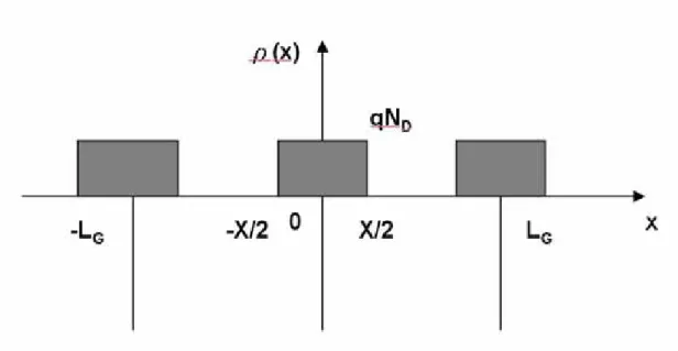
(14) z. Poly-Si film has small grain size,. z. The single crystalline silicon energy band structure is assumed to be applicable inside the crystallites,. z. Doping concentration in poly-Si is uniform,. z. All the doping atoms are ionized,. z. All the grains have the same size, cubic shape,. z. The representation is mono-dimensional,. z. The grain boundaries have no thickness,. z. The defects are carrier traps that are located in the grain boundaries. In this condition, the trap concentration is defined per surface unit. The trap is assumed to be initially neutral and become charged by trapping carriers,. z. The traps are acceptors in the n-type and donors in the p-typed semiconductor,. z. The trap energy level is unique and located more or less in middle of the forbidden band.. Barrier height calculation: We consider the different following parameters: X, extension of the space charge region; ND, donor doping atom concentration; NTA, acceptor like trap surface density at grain boundaries; ε0, permittivity in vacuum; εs, semiconductor permittivity; LG, size of the grain; φ, the electrostatic potential; x, the position coordinate. The distribution of the charges in the material is schematically described Figure 1-2-1. At grain boundaries, the surface trap charge density is qNTA, which thus compensates the charge of the volume ionized doping atom concentration (qND). An abrupt depletion approximation is used to calculate the energy band diagram in the crystallite. 3.
(15) In the space charge region, for. 0 < x<. d 2ϕ. X 2. dx. 2. d 2ϕ. LG X Out of the space charge region, 2 < x< 2. dx 2. =−. qN D. ε rε0. (1-2-1). =0. (1-2-2). Considering that at the border of the space charge region the electric field is null: dϕ X [ dx ]X/2 = 0 for 0< x< 2 L X < x< G 2 2. qN D ⎛ X ⎞ dϕ qN D : dx =− ε s ε 0 x+cst = ε s ε 0 ⎜⎝ 2 − x ⎟⎠ ⎛X⎞. qN. ⎛X. ⎞. 2. ⎛X⎞. D : ϕ (x )=ϕ ⎜ 2 ⎟ : ϕ (x )=− 2ε ε ⎜ 2 − x ⎟ +ϕ ⎜ 2 ⎟ s 0⎝ ⎝ ⎠ ⎝ ⎠ ⎠. Thus the energy barrier height (EB) is defined at grain boundaries as the energy X. difference between the positions x = 0 and x = 2 . 2 2 ⎛ ⎛ X ⎞⎞ q ND ⎛ X ⎞ E B =−⎜⎜ qϕ (0 )−qϕ ⎜ ⎟ ⎟⎟=+ ⎜ ⎟ ⎝ 2 ⎠ ⎠ 2ε s ε 0 ⎝ 2 ⎠ ⎝. E B =+. q2 ND 2 X 8ε s ε 0. (1-2-3). The value of X has to verify for the electrical neutrality of the global material, which means XqND+=qNTA-. NTA- is the ionized part of NTA. The Seto’s model defines a critical concentration (ND*), which corresponds to this limit:. X LG = 2 2. N. * TA → X = LG → N D = L G. (1-2-4). For a fixed trap density, if the effective doping concentration is higher than the critical concentration, the space charge extension is lower than the crystallite site. On the contrary, the crystallite is fully depleted.. ND>ND*. N TA : X= N D. q 2 NTA 2 = + E and B 8ε ε N s 0 D. The expressions of the potential in the both regions are shown as follows:. 4. (1-2-5).
(16) X 0 < x< 2. qN D ⎛ N TA ⎞ −x ⎟ ϕ (x )=− ⎜ 2ε s ε 0 ⎜⎝ 2 N D ⎟⎠. L X < x< G 2 2. ϕ (x )=0. ND<ND*:. X=LG with LGND=NTA. E B =+. 2. q2 N D 2 L 8ε s ε 0 G. (1-2-6). (1-2-7). (1-2-8). The potential variation in the crystallite is expressed by the following:. ϕ (x )=−. 1-3.. qN D ⎛ LG ⎞ − x ⎟⎟ ⎜ 2ε sε 0 ⎜⎝ 2 ⎠. 2. (1-2-9). RPI Model for Poly-Si TFT. The poly-Si TFT models could be divided into three categories: the models that try to incorporate the physics related to individual grain boundaries[14], the models that use close form analytical expressions for current-voltage characteristics[15,16], and the models based on effective medium. In recent years, several models for poly-Si TFTs have been proposed. Lin et al. obtained an expression for grain barrier height as a function of gate bias and the lateral electric field from a quasi-two-dimensional formulation of Poisson’s equation. This solution was incorporated in an expression for the drain current in poly-Si TFTs. Further insight relating the characteristics to the poly-Si material parameters was provided by Fortunato and Magliorato [17]. Other solutions use Poisson’s equation with the inclusion of space charge due to traps. Still others seek formulations with a minimum of empirical approximations. Although useful for the insight they provide, these expressions tend to be too complication for implementation in circuit simulators. The effective medium approach permits the development of comparatively simple models with only a few easily extractable parameters. Although these parameters cannot always be directly related to material 5.
(17) properties, such models are attractive for use in SPICE type circuit simulators. The above models are mainly developed for long-channel poly-Si TFTs although later versions by Jacunski et al. [18,19] have included physics based formulations of important mechanisms such as the kink effect, the field effect mobility in moderate inversion, and the subthreshold current. Finally, the most recent models based on these semi-empirical effective medium approach also include short-channel effects, drain induced barrier lowering (DIBL), velocity saturation, temperature effects, and mobility degradation at high gate bias.[18,20-22] The poly-Si TFT models developed by Jacunski et al.[18] are essentially unified models for long-channel devices. Above threshold, the conducting channel (Ia) in the non-saturated regime is given by an expression similar to that used for long-channel. Vdse W⎛ = − I C V µ ⎜ a FET ox gt ⎜ crystalline MOSFETs: L⎝ 2α sat. ⎞ ⎟⎟Vdse ⎠. (1-3-1). Here, µFET is the gate voltage dependent field-effect mobility that includes the effects of the trap states; Cox=εi/di is the oxide capacitance per unit area, where εi is the dielectric permittivity and di is the thickness of the gate oxide; W and L are the gate width and length, respectively; αsat is the body constant; Vgt ≣ Vgs-VT is the effective extrinsic gate voltage swing, where Vgs and VT are extrinsic gate-source voltage and threshold voltage given by the following interpolation function that tends to Vds in the linear regime and to the saturation voltage Vsat in saturation. Vdse =. Vds ⎛ ⎛V ⎜ 1+⎜ ds ⎜ ⎝ Vsat ⎝. ⎞ ⎟ ⎠. mss ⎞. ⎟ ⎟ ⎠. 1/ mss. (1-3-2). The parameter mss controls the transition at saturation. The above threshold ∂I a. saturation voltage in this model is defined as the value of Vds for which ∂V =0 , ds 6.
(18) which gives. Vsat =(2 )1/ mss α satVgt For the long-channel case, we typically have mss>>1, in which case Vsat~αsat Vgt. Below threshold, the current is dominated by diffusion and is given by: I sub = µ s C ox. ⎛ V gs −VT W ( ηVth )2 exp⎜⎜ L ⎝ ηVth. ⎞⎡ ⎟ ⎢1−exp⎛⎜ −Vds ⎜ ηV ⎟ ⎝ th ⎠⎣. ⎞⎤ ⎟⎟⎥ ⎠⎦. (1-3-3). where η is the subthreshold ideality factor, and µs is subthreshold mobility, and Vth=kBT/q is thermal voltage. A unified model can be obtained for the drain current (Id) by combining the above-threshold and the subthreshold currents as follows:. 1 1 1 = + I d I sub I a. (1-3-4). To make this possible, we extend the range of equation (1-3-1) into the subthreshold regime and retain equation (1-3-3) into the above-threshold regime in such a way that Id approaches the correct limiting behavior in both regimes. This is possible if Vgt in equation (1-3-1) is replaced by the following effective gate voltage overdrive, which is valid above and below threshold:[25,26] ⎡ 2⎤ V gt ⎞ ⎥ ⎢ 2 ⎛⎜ V gt ⎟ V gte =ηVth ⎢1+ + δ + −1 ⎜ 2ηVth ⎟ ⎥ 2ηVth ⎝ ⎠ ⎥ ⎢ ⎣ ⎦. (1-3-5). where δ is a transition parameter with a typical value of about 2. From Eq. (1-3-5), we have Vgte~ηVth below threshold and Vgte~Vgs-VT above threshold. In poly-Si TFTs, not all charge carriers induced in the channel by the gate voltage will be free to contribute to the drain current. Instead, a significant of the carriers will be captured by traps associated with the grain boundaries, especially near and below 7.
(19) threshold. This effect can be taken into account by proposing so-call field effect mobility as follows: 1. µ FET. 1. =. µ1. 2V gte. mu. +. 1. µ0. (1-3-6). ηVth. where mµ, µ0 and µ1 are extractable mobility parameter. Semi-empirical, accounting for feedback and using results from the impact ionization rate theory, the increase of the drain current caused by the kink effect can be modeled as follows[19,22]: ⎛L I kink =⎜⎜ kink ⎝ L. ⎞ ⎟⎟ ⎠. m kink. ⎛ Vds −Vdse ⎜⎜ ⎝ Vkink. ⎞ ⎛ −Vkink ⎟⎟exp⎜⎜ ⎠ ⎝ Vds −Vdse. ⎞ ⎟⎟ I d ⎠. (1-3-7). where Vkink, Lkink and mkink are model parameters, and Id is the primary drain current discussed above.. 1-4.. Motivation. Because the mobility is high as 150 cm2/V-s, the impact ionization current is needed to suppress. Usually we use LDD structure to suppress the Kink effect, the parasitic resistance can lowing the electrical field at drain region. Above these models for Poly-Si Thin Film Transistor, they did not detail to discuss the effect of parasitic resistance. If we use existing SPICE tool to simulate I-V of Thin Film Transistor with LDD structure, the characteristic of drain current would be inaccuracy. We can say that inaccuracy of drain current is due to the lack of the parameters of parasitic resistance. For this reason, we plan to investigate parasitic resistance in different temperature and electrical field. We would analyze the measured data to obtain useful parameters to define some fundamental physical phenomenon such as threshold voltage and effective channel length. In this study, the model of poly-Si TFTs with 8.
(20) LDD structure had been proposed.. 1-5.. Thesis Outline. In the chapter 1, we discuss the effect of trap in the grain boundary and explain the meaning of grain barrier height. The grain barrier height equation is deduced based on the Seto’s model. But it is inapposite for big grain size of thin film transistor. Then we discuss RPI model that is for implementation in a SPICE circuit simulator. The intrinsic DC model describes all four regimes of operation: leakage, subthreshold, above threshold, and kink. In the chapter 2, first we briefly describe poly-Si thin film transistor structure in this study and the main steps of process. We measured different structures of thin film transistor with LDD. The study shows the characteristics of different LDD structure, for example, self align LDD and gate overlap LDD. And we extracted sufficient parameters of parasitic resistance for our model. In the chapter 3, we deduce the LDD model for Poly-Si TFT by using equivalent circuit. In 3-2, the parasitic resistance model was using simulate the characteristic of current in the linear region. Then we discuss the grain barrier model and describe the current model. In the chapter 4, we would discuss the limit of voltage region about these parasitic resistance models.. 9.
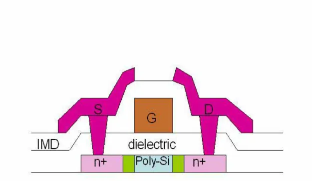
(21) Chapter 2 Characteristics of thin film transistor with different LDD structures 2-1.. Device structure and fabrication process. The figure 2-1-1 shows that cross-sectional view of a poly-Si TFT with self-align LDD. These devices were fabricated on glass substrate with the channel film deposited as amorphous silicon to a thickness of 50 nm. The film was crystallized by excimer laser annealing (ELA). After the device islands were defined, a 100-nm gate oxide was deposited. In this study we need gate overlap LDD and self-align LDD. Therefore, gate overlap region is defined by mask and self-align region is defined by gate metal. We can manufacture different length of GOLDD and SALDD.. 2-2.. Parameter extraction. In this study, the parasitic resistances dominated by the LDD regions are extracted from device characteristics directly. It is well known that the turn-on resistance (RON) for devices operated in linear region can be express as:. RON. ∂V = D ∂I D. VG. = Rch + 2 RP. (2-2-1). VD → 0. where Rch and Rp represent channel resistance and parasitic resistance. The channel resistance in the linear region can be given approximately by:. Rch =. L Wµ 0Cox (VG − VT ). (2-2-2). where Cox is the capacitance per unit area, W, L, and VT are intrinsic channel width, length, threshold and voltage, respectively. VT is defined, for devices with long 10.
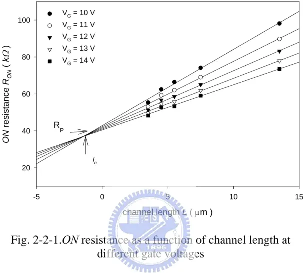
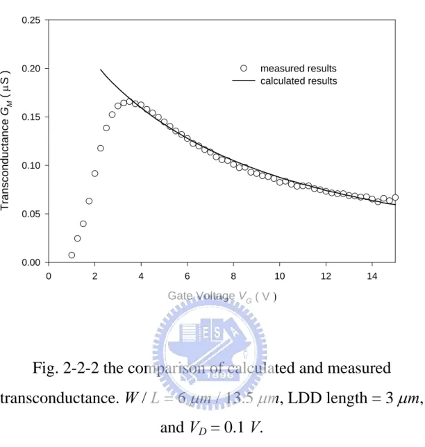
(22) channel length, as the gate voltage when the normalized drain current equal to 10-8 A under small drain bias. With characteristics of devices with different channel length, the parasitic resistance Rp can be extracted by plotting R on ⋅ W versus L as in figure 2-2-1 [23, 24]. It is found that all the lines merge at L = A 0 and has a residual value of gate-voltage independent Rp. A 0 can be considered as a characteristic length that replaces the L to be Lmask- A 0 in our model. The physical meaning of A 0 relates to the carrier redistribution effect when A 0 being larger than zero and represents the current spreading effect when A 0 being negative. The extracted Rp and A 0 for devices with various LDD lengths are listed in Table I. It is found that the extracted Rp value is almost proportional to the LDD lengths. By replacing the extracted Rp and L =Lmask- A 0 into equation 2-2-2, under small drain bias, the transconductance can be written as [23]. GM ≡. ∂I lin Rch ≅ AVD ( )2 ∂VG R p + Rch. = AVD [ AR p (VG − VT ) + 1] where. A≡. (2-2-3). −2. Wµ0Cox . As a result, the intrinsic mobility µ0 can be defined by Lmask − l0. comparing the calculated transconductances and the measured ones under large gate bias and small drain bias as shown in Figure 2-2-2.. 2-3.. Characteristics of device with GOLDD structure. In the section, we would discuss the characteristics of devices with gate overlapped lightly doped drain architecture (GOLDD) structure. For device with 11.
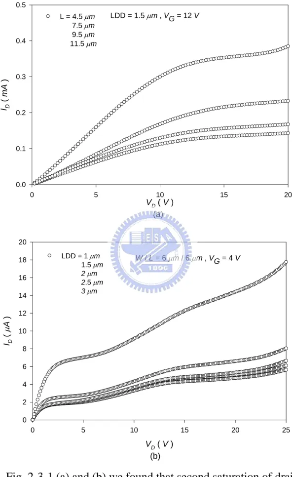
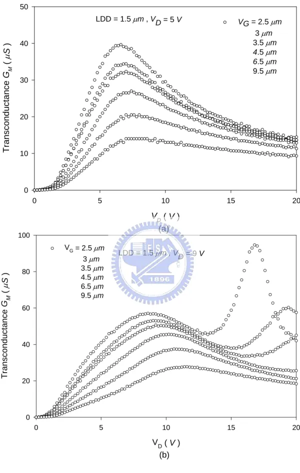
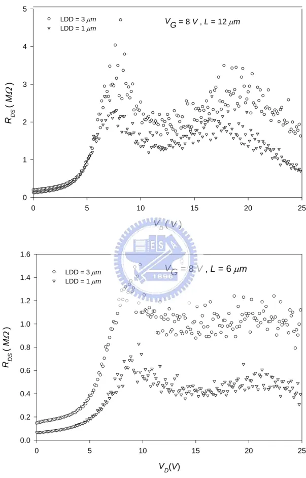
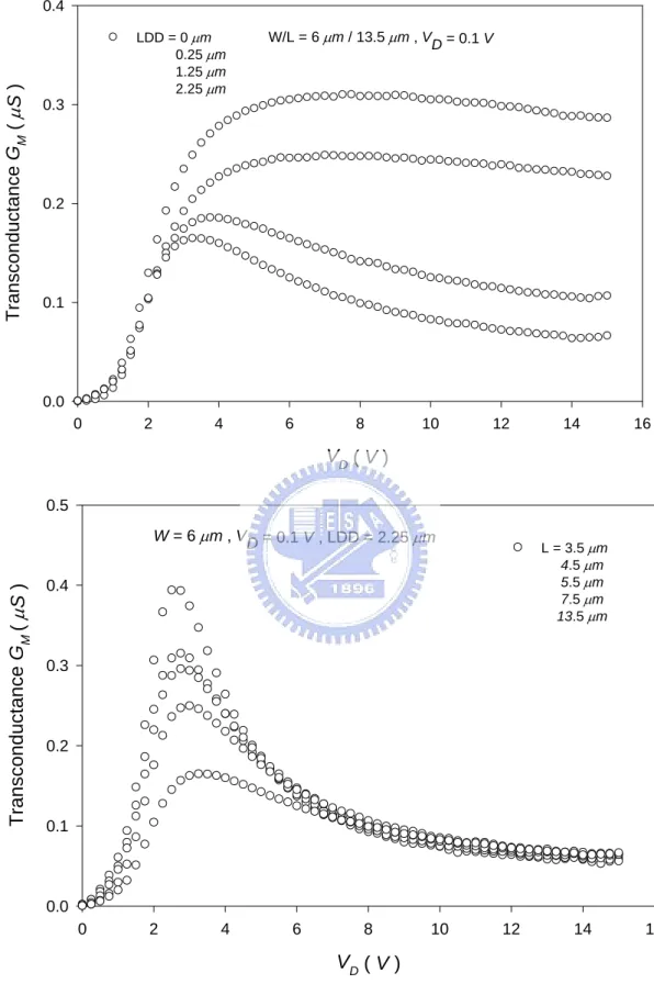
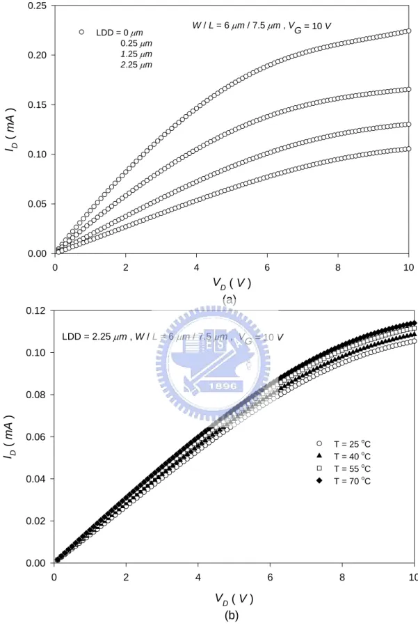
(23) GOLDD in this experiment, the length of gate overlapped lightly doped drain region is 0.75 µm and total lightly doped drain region have seven variable lengths: 0, 0.5, 1, 1.5, 2, 2.5 and 3 µm. In figure 2-3-1 the output characteristics, measured at VG = 4 V, are shown. As can be noted the output characteristics show that there are a second saturation of the drain current for 10 V < VD < 15 V. The second saturation of the drain current previously was discussed [27], and they used two subtransistors model to simulate the output characteristics of the GOLDD TFT. In figure 2-3-2 (a) and (b) show that the transconductance GM of the GOLDD TFT and the two peak were observed at VD = 9 V. In the same way, we also can observe the second saturation of drain current in output resistance, as shown in figure 2-3-3 (a) and (b). In figure 2-3-4 (a) and (b), the length of LDD region would affect the transconductance GM. For both channel length L = 6 µm and 12 µm, the transconductance GM decreased with increasing LDD length.. 2-4.. Characteristics of device with SALDD structure. In this paper, the structure of device that was used to develop TFT model with LDD structure which is self align lightly doped drain structure. First, we introduce the characteristics of TFT with SALDD structure. In figure 2-4-1 (a) and (b), the effect of LDD length and channel length was shown. We found that the transconductance GM would trend to a same value with increasing drain voltage, as shown in figure 2-4-1 (b). The output characteristics of drain were shown in figure 2-4-2 (a), and we observed the effect of grain barrier height dependent on temperature, as shown in figure 2-4-2 (b).. 2-5. Comparison between self-aligned devices and GOLDD devices 12.
(24) After briefly introducing, the characteristics of TFT with SALDD and GOLDD were obviously compared. The GOLDD architecture is more effective in reducing the electrical field of drain region and second saturation of drain current only was observed in GOLDD structure. Therefore, we can understand that the parasitic transistor in gate overlap region can suppress drain field and induce the second saturation. However, the process of GOLDD structure is more complicated than SALDD structure. In order to simplify the analysis of electrical field, we adopted the SALDD structure in this paper. In chapter 3, the LDD model was developed based on SALDD TFT.. 13.
(25) Chapter 3 Poly-Silicon Model for LDD Structure 3-1.. Above-Threshold Model. 3-1-1. Equivalent Circuit of Polysilicon Thin Film Transistor with LDD Structure For devices with LDD structure, the lightly doped regions give rise to large series resistance. The lateral voltage drop across the inversion channel region is therefore not the external drain to source voltage drop (represents by VD when the source is connected to ground) anymore. As a result, the device output characteristics should be modified with this parasitic resistance influence in the LDD regions. By taking into account that the devices are fabricated by a self-aligned process, the source and drain side LDD regions should be almost identical. Therefore, in this proposed model, the source side parasitic resistance and the drain side parasitic resistance are of the same value Rp. From the equivalent circuit as shown in Figure 3-1-1, the internal bias condition across the inversion channel region (e.g., Vds and Vgs) can be express as. Vds = VD − 2RP I D. (3-1-1). Vgs = VG -RP I D. (3-1-2). Therefore, the linear region drain current (Ilin) can be modified as:. I lin =. W 1 ⎡ ⎤ µFETCox ⎢(VGT − I D RP )(VD − 2I D RP ) − (VD − 2I D RP )2 ⎥ L 2 ⎣ ⎦. where. 1. µ FET. =. 1. µ0. +. (3-1-3). 1 2qVGT mµ is the empirical mobility model considering the µ1 ( ) ηkT. gate voltage dependence on effective mobility [28]. µ1, η and mµ are fitting 14.
(26) parameters. µ0 is the intrinsic mobility under high gate bias when the grain barrier no longer influences the carrier transport. The deviation of µFET from µ0 mostly occur when gate voltage is smaller than 10 V and the deviation is about 10~20%. After expansion of Eq. (3), the linear region drain current can be rewritten as. I lin. W 1 µ FET Cox (VG − VT − VD ) ⋅ VD L 2 = W 1 1 + µ FET Cox (VG − VT − V D ) ⋅ 2 R P L 2. (3-1-4). The output current in saturation region (Isat) should take into account the velocity saturation effect and also the channel length modulation effect. According to the simple velocity saturation model proposed by M. Shur [28] for MOSFET devices, the saturation current can be express as:. Isat =. W µFETCox(VG −VT )2(1+λVD) L 2. ⎛V −V ⎞ W W 1+ µFETCoxRP(VG −VT ) + 1+2 µFETCoxRP(VG −VT ) +⎜⎜ G T ⎟⎟ L L ⎝ VL ⎠. (3-1-5). Here, Vsat is the saturation voltage. VL = FsL, where Fs is the saturation field and L is the channel length. λ is the fitting parameter that represents the channel length modulation effect. After the saturation current was decided, Vsat can be defined by. V sat. ⎡ ⎛ V − VT = V G − VT − V L ⎢ 1 + ⎜⎜ G ⎢ ⎝ VL ⎣. 2 ⎤ ⎞ ⎟⎟ − 1⎥ + 2 R P I sat ⎥ ⎠ ⎦. (3-1-6). The total drain current is therefore can be written as. I DS. W 1 µ FET C ox (VG − VT − V DSE ) ⋅ V DSE (1 + λV D ) 2 = L W 1 1 + µ FET C ox (VG − VT − V DSE ) ⋅ 2 R P L 2. 15. (3-1-7).
(27) with V DSE =. VD ⎡ ⎛V ⎢1 + ⎜⎜ D ⎢⎣ ⎝ V sat. ⎞ ⎟⎟ ⎠. m ss. ⎤ ⎥ ⎥⎦. (3-1-8). 1 m ss. where mss is a parameter that determines the shape of the characteristics in the knee region. Then, the channel length modulation coefficient λ can be defined by comparing saturation current Isat with measured one. After calculating the corresponding saturation voltage Vsat, the total output drain current is obtained. Figure 3-1-2 (a) and 3-1-2 (b) depict the calculated results and the measured results for devices with different LDD length (LDD length = 1µm and 3 µm, respectively). Good agreements are found when comparing these two results. The related parameters are listed in Table II. Figure 3-1-3 (a) and 3-1-3 (b) compares the calculated and the measured conductance GD and ON resistance RON, respectively. It is found that the parameters related to kink effect can be defined more accurately by comparing the calculated RON and the measured one as shown in figure 3-1-3 (b). The results are listed in Table III for devices with different LDD length. Finally, the kink effect was considered by adding. I kink. ⎛L ⎞ = ⎜ kink ⎟ ⎝ L ⎠. mkink. ⎛ VD − VDSE ⎜⎜ ⎝ Vkink. ⎞ − Vkink ⎟⎟ exp( ) I DS V − V D DSE ⎠. (3-1-8). into Equation 3-1-7 [28, 29], where Vkink, Lkink and mkink are model parameters. For devices with channel length longer than 6 µm, the kink effect is not a pronounced factor. It should be taken into consideration only when comparing the calculated RON and the measured one. Noticeably, the scattering effect is not included in this model. The calculated and 16.
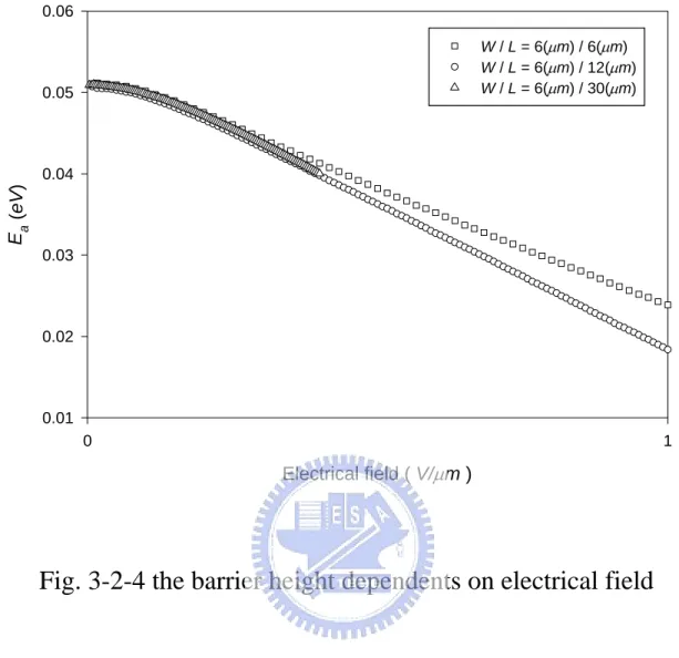
(28) simulated GM for devices with different channel lengths are depicted in figure 3-1-4 (a) and 3-1-4 (b). It is found that the degradation of GM under large gate bias is more pronounced for devices with short channel length. This is due to the influence of large parasitic resistance for short-channel devices. It can be concluded that our model reproduces device characteristics very well not only in a large range of bias condition but also for devices with various LDD length and channel length.. 3-2.. DIBL in LDD region. Although we use simple equivalent circuit to obtain LDD model in 3-1, we can not explain some phenomenon. For example, at high gate voltage and low drain voltage condition, we found that the I-V characteristic of device which was operated in linear region is curved. If parasitic resistance is constant, the characteristic of linear region would be straight. Therefore parasitic resistance may be not constant. In 3-2, we try to prove that the value of resistance is variable and dependent on temperature. First, we focus on the measurement of resistant testkey at different temperature. Figure 3-2-1 show that current vs. voltage plots for with W/L = 3 (µm)/3 (µm) and W/L = 6 (µm)/6 (µm). In figure 3-2-1 (a) and (b) show current as a function of voltage at different temperature. We found that the value of resistance would change depend on voltage and temperature. The figure 3-2-2 (a) and (b) show that plot of RON as a function of voltage for resistance testkeys with W/L = 3 (µm)/3 (µm) and W/L = 6 (µm)/6 (µm). We observed for all devices that RON decrease with increasing temperature. It is obvious that the grain barrier exists in resistance. We can construct a plot of activation energy at a function of gate voltage, as given in figure 3-2-3 (a) and (b). Therefore, the resistance equation which includes the grain barrier height model was considered to be defined as: 17.
(29) ⎛E R= R0 exp⎜⎜ B ⎝ kT. ⎞ ⎟⎟ ⎠. (3-2-1). We found EB that it depends on electrical field, as shown in figure 3-2-4. Hence, EB can be extracted from that activation energy barrier slope varies with applied voltage in figure 3-2-5. We defined EB equation as:. E B = Ea − S. V LDD. (3-2-2). where Ea is the barrier height at voltage V = 0, S is the slope of the linear regression and LDD is the length of resistance. On the side, when the value of extra voltage V is very high, the value of resistance would be tending towards a constant. Finally, we need an equation to combine the different regions. The effective resistance was calculated according to the following equation: ⎡ V ⎞ ⎢ ⎛⎜ ⎛ ⎜ E a −S ⎟ LDD ⎟ ⎢1+⎜ RLOW REFF = R0 exp⎜ ⎢ ⎜ kT ⎛E ⎜ ⎟⎢ ⎜ ⎜ ⎟ R exp⎜ B ⎝ ⎠⎢ ⎜ 0 ⎝ kT ⎣⎢ ⎝. ⎞ ⎟ ⎟ ⎞ ⎟⎟ ⎟⎟ ⎠⎠. 3⎤. 1/ 3. ⎥ ⎥ ⎥ ⎥ ⎥ ⎦⎥. (3-2-3). RLOW was defined as the lowest of resistance value. R is the effective resistance given by the following interpolation function that tends to R in low voltage and to RLOW in high voltage. In the following, we need the correct voltage which drops across the parasitic resistance in TFT device with LDD structure. Because the value of drain current which passes LDD region and channel region is same, we use equation (3-2-3) and MOSFET current equation to deduce the value of voltage in the LDD region. The figure 3-2-6 shows that voltage in LDD region dependent on drain voltage. The variation of parasitic resistance dependent on drain voltage was showed in the figure 3-2-7. 18.
(30) ⎡ ⎛ ⎢ ⎜ ⎢ ⎜ ⎢ ⎜ ⎢ ⎜ R LOW V * ⎢1+⎜ V V ⎞ ⎢ ⎜ ⎛ ⎛ ⎜ E a −S ⎟ ⎢ ⎜ ⎜ Ea −S LDD LDD ⎟ ⎢ ⎜ R0 exp⎜ R0 exp⎜ kT kT ⎜ ⎟ ⎢ ⎜ ⎜ ⎜ ⎟ ⎜ ⎝ ⎠ ⎢ ⎝ ⎝ ⎣. ⎞ ⎟ ⎟ ⎟ ⎟ ⎟ ⎞⎟ ⎟⎟ ⎟⎟ ⎟⎟ ⎟ ⎠⎠. 3⎤. −1/ 3. ⎥ ⎥ ⎥ ⎥ ⎥ ⎥ ⎥ ⎥ ⎥ ⎥ ⎦. −. 1 W ⎡ ⎤ *µ * (V −V −V )(V D −2V )− (VD −2V )2 ⎥ =0 2 L FET ⎢⎣ G T ⎦. (3-2-4) Resistance R is replaced by REFF (3-2-3) in equation (3-1-4).. I=. W 1 ⎛ ⎞ C ⎜V −V − V ⎟V µ L FET OX ⎝ G T 2 D ⎠ D ⎡ ⎛ ⎢ ⎜ ⎛ E B ⎞ ⎢ ⎜ R LOW W 1 ⎞ ⎛ C ⎜V −V − V ⎟* 2 R0 exp⎜⎜ µ ⎟⎟* ⎢1+⎜ L FET OX ⎝ G T 2 D ⎠ ⎝ kT ⎠ ⎢ ⎜ R exp⎛⎜ E B ⎜ kT ⎢ ⎜ 0 ⎝ ⎢⎣ ⎝. ⎞ ⎟ ⎟ ⎟ ⎞⎟ ⎟⎟ ⎟ ⎠⎠. 3⎤. ⎥ ⎥ ⎥ ⎥ ⎥ ⎦⎥. 1/ 3. (3-2-5) +1. The results were shown in figure 3-2-8 (a) and (b). We can observe that the characteristics of linear region match measured data. Therefore, we prove that the value of parasitic resistance is variable and depends on the voltage and temperature.. 3-3.. Grain Barrier Height Model. Equation (3-3-1) is the well-know grain boundary barrier height model proposed firstly by Seto et al.[13]. EB represents the grain boundary barrier energy in above-threshold region. NT represents the effective grain boundary trap density and n is the gate-induced carrier density. When there is no other temperature-sensitive mechanism, the measured activation energy could be served as the grain boundary energy barrier. EB =. qNT 2 8εn. (3-3-1). In our experiment, the measured activation energy versus bias drain voltage is plotted 19.
(31) in figure 3-3-1. When drain voltage is high, it has been proposed that the drain-induced grain barrier lowering (DIGBL) effect would influence carrier transport seriously [30, 31, 32]. When the device is operated in the linear region and the drain voltage is low, the barrier increases with increasing drain voltage. This can be explained by the influence of drain bias on the surface potential along the channel. The average carrier density is therefore expressed as:. n=. (. Cox VG −V fb −αVD. ) (3-3-2). qtch. where Cox is capacitance per unit area, Vfb is the flatband voltage, and α is a parameter indicating the influence of drain voltage. tch is the channel thickness. According to the grain boundary barrier height given by Ref. [33], the barrier height considering the influence of the drain voltage and the DIGBL effect is given by VD ] L EB = 8ε s Cox (VG − VT − αVDSe ) tch [(qNT ) 2 − 4qNT ε sη. (3-3-3). For MOSFET devices, the channel thickness is reversely proportional to the gate bias and can be expressed as:. t ch = 8. εs Vth tox ε ox VG − VT. (3-3-4). where tox is the oxide thickness and Vth is thermal voltage. However, in poly-Si TFTs, the channel thickness would be further affected by the screening effect of trapped charges. So we modified the channel thickness as:. ⎛ Vth ⎞ ⎟⎟ tch = 8⎜⎜ ⎝ VG − Vt ⎠. γ −1. tox. εs ε ox. (3-3-5). where γ is the parameter that represents the trapped charge screening effect. Finally,. 20.
(32) grain barrier height model of polysilicon TFT is expressed as: V ⎞ ⎛ t ox ⎜⎜ q 2 N T 2 −4 qN T ε sη D ⎟⎟Vth γ −1 L ⎠ EB = ⎝ ε ox ε s C ox (VG −VT −αV DSe )γ. (3-3-6). Parameter extraction:. γ, VT, NT extraction: using long channel length device (ex. L = 30 um). Under small VD bias. Firstly, γ can be defined by best fitting of the EB vs. VG curve as in figure 3-3-2 (a) and figure 3-3-2 (b). It is found that γ is closer to 2 when the film property is better. This prove the above screening effect mechanism. Table IV lists values of γ for different grain growth conditions. Then the plot of EB-1/γ vs. VG is shown in figure 3-3-3. The VT and NT can be extracted from the x-axis intersection and the slope of the curve. Figure 3-3-4 (a) shows that the line merges at x-axis. The value of x-axis is defined as threshold voltage VT.. α,η extraction: By increasing VD bias, the x-axis intersection of the EB-1/γ vs. VG curve will shift to larger x value. This relationship gives the α value. As seen in figure 3-3-4 (b) the value which merges at x-axis is defined as α. After the determination of. γ, VT, NT and α, η can be obtained by calculation from the experimental data. The related parameters are listed in Table IV. After defining the grain boundary barrier height model, the mobility model can be defined as. 1 µFET. ≡. 1 + µG. 1 ⎛ − EB ⎞ µ0 exp⎜ ⎟ ⎝ kT ⎠. (3-3-7). µ0 represents the intrinsic mobility in the grain region; µG stands for the influence of scattering effect on mobility under large gate voltage. As temperature increases, the field effect mobility µFET increases without incorporating other empirical equations. Finally, we combine the proposed mobility model in equation (3-3-7) into the I-V model in equation (3-1-7). The calculated results and the measured results for devices 21.
(33) with different LDD lengths are depicted in figure 3-3-5 (a) and figure 3-3-5 (b). Good agreement is found in figure 3-3-5 (a), which verifies our proposed model. Some under-estimation is observed in figure 3-3-5 (b). This is due to the voltage dependence of LDD resistance that need to be further studied in our future work.. 22.
(34) Chapter 4 Conclusion The Poly-Si TFT model with self-align LDD was successfully developed and the parameters of parasitic resistance and grain barrier height were extracted from characteristics of devices. The results would be obtained and discussed as follows:. 4-1.. Parameters of parasitic resistance in device. We used the characteristic of TFT device which was operated at linear region to extracting the parasitic resistance value. In order to ignore the effect of drain voltage, we needed a large gate voltage. However, excessive gate voltage would cause the decreasing of parasitic resistance and damage the gate oxide interface. The range of gate voltage has to carefully be determined. In different devices, we have different range of gate voltage to extract the parasitic resistance. On the side, the resistance was extracted from low drain voltage which can not represent correct at any drain voltage.. 4-2.. LDD model of TFT device First we tried to use the present mobility model to combine our model. But. present mobility model can not dependent on gate voltage very well. Therefore we adopted the empirical mobility model to fit the real mobility. In 3-1 section, we can saw that the empirical mobility model predict correctly the characteristics of TFT device with LDD structure. Next step, the variable resistance was used to simulate the characteristic of TFT with LDD structure. The grain barrier height was observed in resistance testkey and we extracted the EB from I-V plots. Because the resistance model includes exponential term, we can not obtain an analytical solution. The modified LDD model can improve accuracy of linear region. Finally, we consider the. 23.
(35) grain barrier which exits in channel region of device. We demonstrated the poly-Si TFT modeling incorporating with the experimentally defined grain barrier height model. It was also found that bias condition and film property had influences on grain barrier and therefore strongly affected the device characteristics. When comparing the experimental results and the simulated results, good agreements were found for devices with different channel length and LDD lengths.. 24.
(36) References [1]A. G. Lewis, I-W. Wu, T. Y. Huang, A. Chiang, and R. H. Bruce, “Active matrix liquid crystal display design using low and high temperature processed polysilicon TFTs,’’ in IEDM Tech. Dig., 1990,pp.843-846 [2]Y. Matsueda, M. Ashizawa, S. Aruga, H. Ohshima, and S. Morozumi, “New technologies for compact TFT LCDs with high-aperture ratio, ’’soc. Information Display, Tech. Dig., pp, 315-318, 1990. [3]R. G. Stewart, S. N. Lee, A. G. Ipri, D. L. Jose, D. A. furst, S. A. Lipp, and W. R. Roach, “A 9V polysilicon LCD with integrated gray-scale drivers,” soc. Information Display, Tech. Dig., pp, 319-322, 1990. [4]T. Yamanaka, T. Hashimoto, N. Hasegawa, T. Tanaka, N. Hashimoto, A. Shimizu, N. Ohki, K. Ishibashi, K. Sasaki, T.Nishida, T. Mine, E. Takeda, and T. Nagano, ”Advanced TFT SRAM Cell Technology Using a Phase-Shift Lithography,’’ IEEE Trans. Electron Devices, Vol. 42, No. 7, pp.1305-1313, 1995. [5]S. D. S. Malhi, H. Shichijio, S.K. Banerjee, R. Sundaresan, M. Elahy, G. P. Polack, W. F. Richardaon, A. h. Shah, L. R. Hite, R. H. Womoack, P. K. Chatterjee, and H. W. Lan, “Characteristics and Three-Dimenssional Integration of MOSFETs in Small-Grain LPCVD Polycrystalline Silicon,’’ IEEE Trans. Electric Devices, Vol.32, No.2, pp.258-281, 1985. [6]K. YoShizaki, H. Takahashi, Y. Kamigaki, T.Yasui, K. Komori, and H. Katto, ISSCC Digest of tech. Papers, p.166, February 1985. [7]N. D. Young, G. Harkin, R. M. Bunn, D. J. McCullloch, and I.D. French, “The Fabrication and Characteristization of EEPROM Arrays on Glass Using a Low-Temperature Poly-Si TFT Process,’’ IEEE Trans. Electron Devices, Vol. 43, 25.
(37) NO.11, pp.1930-1936, 1996. [8]T. Kaneko, Y. Hosokawa, M. Tadauchi, Y. Kita, and H. Andoh, “400 dpi Integrated Contact Type Linear Image Sensors with poly-Si TFT’s Analog Readout Circuits and Dynamics shift Registers,” IEEE Trans. Electron Devices, Vol.38, No.5 ,pp.1086-1039,1991. [9]Y. Hayashi, H. Hayashi, M. Negishi, T. Matsushita, “A Thermal Printer Head with Cmos Thin-Film Transistors and Heating Elements Integrated on a Chip,’’ IEEE Solid-State Circuits Conference (ISSCC), p.266, 1998. [10]N.. Yamauhchi,. Y.. Inaba,. and. M.. Okamamura,. “An. Integrated. Photodector-Amplifier using a-Si p-i-n Photodiodes and Poly-Si Thin Film Transistors, ’’ IEEE Photonic Tech. Lett., Vol.5, p.319, 1993. [11]M. G. Clark, “Current Status and Future Propects of Poly-Si,’’ IEEE proc. Circuits Devices Syst., Vol. 141, No.1, p3.3, 1994. [12]K. Nakazawa, J. Appl. Phys., 69(3), pp.1703, 1992. [13] J. Y. Seto, “The electrical properties of polycrystalline silicon films,” J. Appl. Physics, 46, 5247, (1975) [14]P.-S. Lin, J-Y. Guo, and C.-Y. Wu, “A Quasi-Two Dimensional Analytical Model for the Turn-On Characteristic of polysilicon Thin-Film Transistors,’’ IEEE Trans. On Electron Devices, 37 (3), 666-674 (1990). [15]S. Chen, F. Shone, and J. Kuo, “A closed form inversion type polysilicon thin-film transistor DC/AC model consonsidering the kink effect,’’ J. Appl. Phys., 77, 1776(1995). [16]H. Chern, C. Lee, and T. Lei, “An analytical model for the above threshold characteristics of polysilicon thin-film transistors,’’ IEEE Trans. Electron Devices, 26.
(38) 42, 1240(1995). [17]G. Fortunate and P. Migliorato, ”Model for the abovethreshold characteristics and threshold voltage in polysilicon thin-film transistors,” J. Appl. Phys., 68, 2463(1990). [18] M. Jacunski, “Characterization and Modeling of Short-Channel Polysilicon Thin Film Transistors,’’ Ph. D. Dissertation University of Virginia, 1997. [19] M. Jacunski, M. shur, and A. A. Owusu, T Ytterdal, M. Hack, and B. iniguez, “A Short Channel DC SPICE Model for Polysilicon Thin Film Transistors Including Temperature Effects,’’ IEEE Trans. on Electron Devices, 46(6), 1146-1158(1999). [20]S. S. Sung, D. C. Chen, C. T. Cheng and C. F. Yeh, “ A physically-Based Built-in Spice Poly-Si TFT Model for Circuit Simulation and Reliability Evaluation,’’ Proceedings of IEDM, 139-142, December 1996. [21]M. D. Jacunski, M. shur, T. Ytterdal, A OWusu, and M. Hack, “AC and DC Characterization and SPICE Modeling of Short-Channel Polysilicon TFT’s,’’ presented at 1996 Mater. Res. Soc. Spring Meet., San Francisco, Ca., Apr. 1996. [22]B. Iniguez, Z. Xu, T. A. Fjeldly, and M. Shur, “Unified Model for short-Channel Poly-Si TFTs,’’ Solid-State Electronics, 43, 1821-1831(1999). [23]Hsiao Wen Zan, Ting-Chang Chang, Po-Sheng Shih, Du-Zen Peng, Po-Yi Kuo, Tiao-Yuan Huang, Chun Yen Chang, and Po-Tsun Liu, “A Study of Parasitic Resistance Effects in Thin-Channel Polycrystalline Thin-Film Transistors with Tungsten-Clad Source/Drain,” IEEE Electron Device Letters., pp. 509-511, Aug. 2003. [24]Shengwen Luan and Gerold W. Neudeck, “An experimental study of the source/drain parasitic resistance effects in amorphous silicon thin film transistors,” J. Appl. Phys., Vol. 72, No. 2, 15 July 1992. 27.
(39) [25]K. Lee, M. Shur, T. A. Fjeldy and T. Ytterdal , Semiconductor Device Modeling for VLSI, Prentice-Hall, 1993. [26] T. A. Fjeldy, T. Ytterdal and M. Shur, Introduction to Device Modeling and Circuit Simulation, New York: John Wiley & Sons, 1998. [27] A. Bonfiglietti, M. Cuscuna, A Valletta, L. Mariucci, A. Pecora, G. Fortunato, S. D. Bortherton, and J. R. Ayres “Analysis of. Electrical Characteristics of Gate. Overlapped Lightly Doped Drain (GOLDD) Polysilicon Thin-Film Transistors With Different LDD Doping Concentration,” IEEE Transactions On Electron Devices, Vol. 50, No.12, 2003 [28] Michael Shur “SEMICONDUCTOR DEVICE MODELING FOR VLSI” Prentice Hall International 1993 [29] Benjamin Iniguez, “Unified model for short-channel poly-Si TFTs,” Solid-State Electronics 43 1999 [30] P. S. Lin, Jwin-Yen Guo and Ching-Yuan Wu,“A quasi-two-dimensional analytical model for the turn-on characteristics of polysilicon thin-film transistors,” IEEE Trans. Electron Devices, Vol. 37, No. 3, March 1990 [31] H. L. Chen and Ching-Yuan Wu, “A New I-V Model Considering the Impact-Ionization Effect Initiated by the DIGBL Current for the Intrinsic n-Channel Poly-Si TFT’s,” IEEE Trans. Electron Devices, Vol. 46, No. 4, April 1999 [32] R. E. Proano, R. S. Misage and D. G. Ast, ”Development and Electrical Properties of Undoped Polycrystalline Silicon Thin-Film Transistors” IEEE Transaistors on Electron Devices. VOL.36. September 1989 [33] Gi-Young Yang; Sung-Hoi Hur; Choong-Ki Kim; Chul-Hi Han, “A Physical-Based Analytical Turn-On Model of Polysilicon Thin Film Transistors for Circuit Simulation,” IEDM, pp.953-956 1995. 28.
(40) Table 3-1 Extracted RP and l0 for devices with different LDD lengths LDD. 0 µm. 1 µm. 2 µm. 3 µm. RP ( ohm ). 1000. 2500. 16000. 32000. L0( µm ). 2.5. 0.5. -1. -1.5. 29.
(41) Table 3-2 Key parameters extracted for the proposed model Parameter. Definition. Units. Value. µ0. High field long-channel zero-bias mobility Long-channel zero-bias threshold voltage. cm2/Vs. 150. V. 1.7. Vt mss. Vdse transition parameter. µ1. Low field mobility. mµ. Low field mobility exponent. 1.4. η. Zero-bias ideality factor. 7. vs = µ0Fs. Saturation velocity. 30. 4 cm2/Vs. cm/s. 15. 1.5×10⁶.
(42) Table 3-3 Parameters related to kink effect for devices with different LDD lengths LDD. 1 µm. 2 µm. 3 µm. Lkink. 1.5 µm. 1.5 µm. 1.5 µm. mkink. 0.01. 0.01. 0.1. Vkink. 11 V. 11 V. 9V. 31.
(43) Table 3-4 Key Parameters of Grain Barrier Model for devices with different film properties. NT ( 1012cm-2 ). VT ( V ). 1. 2.33. 5.945. 1. 1.95. 3. 1.3. 1.93. 2.98. 1.3. 1.89. 0.41. 1.3. 1.51. 0.27. 1.55. 0.6. 0.26. γ As-Deposited (plasma=0 Hrs) As-Deposited (plasma=2 Hrs) SPC (plasma=0 Hrs) SPC (plasma=1 Hrs) SPC (plasma=2 Hrs) ELA. 32.
(44) Figure 1-2-1. Simplified distribution of charges within the grain and at grain boundaries. At grain boundaries, the trap state density is defined per surface unit, while ND is a doping volume concentration.. 33.
(45) Fig. 2-1-1.Polysilicon TFT device structure. 34.
(46) VG = 10 V. 100. VG = 11 V. ON resistance RON ( kΩ ). VG = 12 V VG = 13 V. 80. VG = 14 V. 60. RP. 40. lo. 20. -5. 0. 5. 10. channel length L ( µm ). Fig. 2-2-1.ON resistance as a function of channel length at different gate voltages. 35. 15.
(47) Transconductance GM ( µS ). 0.25. measured results calculated results. 0.20. 0.15. 0.10. 0.05. 0.00 0. 2. 4. 6. 8. 10. 12. 14. Gate Voltage VG ( V ). Fig. 2-2-2 the comparison of calculated and measured transconductance. W / L = 6 µm / 13.5 µm, LDD length = 3 µm, and VD = 0.1 V.. 36.
(48) 0.5. L = 4.5 µm 7.5 µm 9.5 µm 11.5 µm. ID ( mA ). 0.4. LDD = 1.5 µm , VG = 12 V. 0.3. 0.2. 0.1. 0.0 0. 5. 10. 15. 20. VD ( V ) (a) 20 LDD = 1 µm 1.5 µm 2 µm 2.5 µm 3 µm. 18 16. ID ( µA ). 14. W / L = 6 µm / 6 µm , VG = 4 V. 12 10 8 6 4 2 0 0. 5. 10. 15. 20. 25. VD ( V ) (b). Fig. 2-3-1 (a) and (b) we found that second saturation of drain current at VG = 4 V 37.
(49) 50. Transconductance GM ( µS ). LDD = 1.5 µm , VD = 5 V. VG = 2.5 µm 3 µm 3.5 µm 4.5 µm 6.5 µm 9.5 µm. 40. 30. 20. 10. 0 0. 5. 15. 20. 15. 20. VD ( V ) (a). 100. VG = 2.5 µm. Transconductance GM ( µS ). 10. 3 µm 3.5 µm 4.5 µm 6.5 µm 9.5 µm. 80. LDD = 1.5 µm , VD = 9 V. 60. 40. 20. 0 0. 5. 10. VD ( V ) (b). Fig. 2-3-2 show that the transconductance GM of the GOLDD. TFT and the two peak were observed at VD = 9 V. 38.
(50) 5 LDD = 3 µm LDD = 1 µm. VG = 8 V , L = 12 µm. RDS ( MΩ ). 4. 3. 2. 1. 0 0. 5. 10. 15. 20. 25. VD ( V ) 1.6. VG = 8 V , L = 6 µm. LDD = 3 µm LDD = 1 µm. 1.4. RDS ( MΩ ). 1.2 1.0 0.8 0.6 0.4 0.2 0.0 0. 5. 10. 15. 20. 25. VD(V). Fig. 2-3-3 we can observe the second saturation of drain current in output resistance 39.
(51) 10. Transconductance GM ( µS ). LDD = 3 µm , V = 5 V D. L = 6 µm L = 12 µm. 8. 6. 4. 2. 0 0. 5. 10. 15. 25. 30. VG ( V ) (a). 20. LDD = 1 µm , V. 18. Transconductance GM ( µS ). 20. D=5V. L = 6 µm L = 12 µm. 16 14 12 10 8 6 4 2 0 0. 5. 10. 15. 20. 25. 30. VG ( V ) (b). Fig. 2-3-4 the length of LDD region would affect the transconductance GM. For both channel length L = 6 µm and 12 µm, the transconductance GM decreased with increasing LDD length 40.
(52) Transconductance GM ( µS ). 0.4 LDD = 0 µm 0.25 µm 1.25 µm 2.25 µm. W/L = 6 µm / 13.5 µm , V = 0.1 V D. 0.3. 0.2. 0.1. 0.0 0. 2. 4. 6. 8. 10. 12. 14. 16. VD ( V ) 0.5. Transconductance GM ( µS ). W = 6 µm , VD = 0.1 V , LDD = 2.25 µm. L = 3.5 µm 4.5 µm 5.5 µm 7.5 µm 13.5 µm. 0.4. 0.3. 0.2. 0.1. 0.0 0. 2. 4. 6. 8. 10. 12. 14. 16. VD ( V ). Fig. 2-4-1 the effect of LDD length and channel length was shown. 41.
(53) 0.25 LDD = 0 µm 0.25 µm 1.25 µm 2.25 µm. ID ( mA ). 0.20. W / L = 6 µm / 7.5 µm , V. G = 10 V. 0.15. 0.10. 0.05. 0.00 0. 2. 4. 6. 8. 10. VD ( V ) (a) 0.12 LDD = 2.25 µm , W / L = 6 µm / 7.5 µm , VG = 10 V. 0.10. ID ( mA ). 0.08. 0.06. T = 25 oC T = 40 oC T = 55 oC o T = 70 C. 0.04. 0.02. 0.00 0. 2. 4. 6. 8. 10. VD ( V ) (b). Fig. 2-4-2 (a) show that the I-V curve of drain current with different LDD length and (b) show that drain current increases with increasing temperature. 42.
(54) Fig.3-1-1 equivalent circuit. 43.
(55) 100. LDD = 3 µm, W / L = 6 µm / 13.5 µm. Drain Current ID ( µA ). 80. VG = 12 V 10 V 8V 6V 4V. 60. 40. 20. 0 0. 2. 4. 6. 8. 10. Drain Voltage VD ( V ). Drain Current ID ( µA ). (a). 140. LDD = 1 µm, W / L = 6 µm / 13.5 µm. 120. VG = 12 V 10 V 8V 6V 4V. 100 80 60 40 20 0 0. 2. 4. 6. 8. 10. Drain Voltage VD ( V ) (b). Fig.3-1-2 Above-threshold experimental (symbols) and simulated (solid line) I-V characteristics for poly-Si TFTs with different LDD lengths. 44.
(56) 16. LDD = 3 µm, W / L = 6 µm / 13.5 µm. Conductance GD ( µS ). 14. VG = 12 V 10 V 8V 6V 4V. 12 10 8 6 4 2 0 0. 2. 4. 6. 8. 10. Drain Voltage VD ( V ) (a) 1200. LDD = 3 µm W / L = 6 µm /13.5 µm. VG = 4 V 6V 8V. ON resistance RON ( MΩ ). 1000. 800. 600. 400. 200. 0 0. 2. 4. 6. 8. 10. Drain Voltage VD ( V ) (b). Fig.3-1-3 The calculated and measured conductance GD and ON resistance RON.. 45.
(57) Transconductance GM ( µS ). 8. LDD = 3 µm, W/L =6 µm / 13.5 µm. VD = 4.1 V 3.1 V 2.1 V 1.1 V 0.1 V. 6. 4. 2. 0 0. 2. 4. 6. 8. 10. 12. 14. Gate voltage VG ( V ) (a) 12. LDD = 3 µm, W/L = 6µm / 7.5µm. VD = 4.1 V 3.1 V 2.1 V 1.1 V 0.1 V. Transconductance GM ( µS ). 10. 8. 6. 4. 2. 0 0. 2. 4. 6. 8. 10. 12. 14. Gate voltage VG ( V ) (b). Fig.3-1-4 Above-threshold experimental (symbols) and calculated (solid) transconductance of LDD-TFTs with different channel length.. 46.
(58) W / L = 3(µm) / 3(µm) 0.25 T = 25 oC T = 40 oC T = 55 oC T = 70 oC T = 85 oC. 0.20. I ( mA ). 0.15. 0.10. 0.05. 0.00 0. 1. 2. 3. 4. 5. 6. VD ( V ) (a). W / L = 6(µm) / 6(µm) 0.20 T = 25 oC T = 40 oC T = 55 oC T = 70 oC T = 85 oC. I ( mA ). 0.15. 0.10. 0.05. 0.00 0. 1. 2. 3. 4. 5. 6. VD ( V ) (b). Fig.3-2-1 (a) and (b) show that drain current increase with increasing temperature 47.
(59) W/L = 3(µm) / 3(µm) 70. T = 25oC o T = 40 C T = 55oC o T = 70 C T = 85oC. 60. RON ( kΩ ). 50. 40. 30. 20. 10. 0 0. 1. 2. 3. 4. 5. 6. VD ( V ) (a). W/L = 6(µm) / 6(µm) 70. 60. T = 25oC T = 40oC T = 55oC T = 70oC o T = 85 C. RON ( kΩ ). 50. 40. 30. 20. 10. 0 0. 1. 2. 3. 4. 5. 6. VD ( V ) (b). Fig.3-2-2 (a) and (b) show that ON resistance increase with increasing temperature 48.
(60) W / L = 3(µm) / 3(µm) 0.06. 0.05. Ea ( eV ). 0.04. 0.03. 0.02. 0.01. 0.00 0. 2. 4. 6. 8. 10. VD ( V ) (a). W / L = 6(µm) / 6(µm) 0.06. 0.05. Ea ( eV ). 0.04. 0.03. 0.02. 0.01. 0.00 0. 2. 4. 6. 8. 10. VD ( V ) (b). Fig.3-2-3 the barrier height can be extracted from I-V at different temperature 49.
(61) 0.06 W / L = 6(µm) / 6(µm) W / L = 6(µm) / 12(µm) W / L = 6(µm) / 30(µm). 0.05. Ea (eV). 0.04. 0.03. 0.02. 0.01 0. 1. Electrical field ( V/µm ). Fig. 3-2-4 the barrier height dependents on electrical field. 50.
(62) W / L = 6( µm ) / 6 ( µm ) 0.06. Linear Regression Line measured results 0.05. Ea ( eV ). 0.04. 0.03. 0.02. 0.01. 0.00 0. 1. Electrical field ( V/µm ). Fig.3-2-5 parameters of barrier height were extracted from linear regression line. 51. 2.
(63) 56. LDD = 2.75 ( µm ). 54. VG = 6 V 9V 12 V 15 V. Resistance ( k Ω ). 52 50 48 46 44 42 40 38 0. 1. 2. 3. VD ( V ). The Fig. 3-2-6 shows that voltage in LDD region dependent on drain voltage. 52.
(64) 25 VG = 15 V 12 V 9V 6V. ID ( µA ). 20. LDD = 2.75 µm , W/L = 6 µm /13.5 µm. 15. 10. 5. 0 0. 1. 2. 3. VD ( V ). Fig. 3-2-7 the variation of parasitic resistance dependent on drain voltage was showed. 53.
(65) 0.05 VG = 4 V VG = 6 V. Drain Current Activation Energy ( eV ). 0.04. VG = 8 V VG = 10 V VG = 12 V. 0.03. 0.02. 0.01. 0.00. -0.01 -2. 0. 2. 4. 6. 8. 10. 12. Drain Voltage VD ( V ). Figure 3-3-1 The relationship of activation energy versus drain voltage for different gate voltages. The solid lines represent the simulated result and the symbols represent the experimental data (W/L = 6µm /13.5µm). 54.
(66) 0.8 0.7. EB~(VG-VT)-1. 0.6. EB ( eV ). 0.5 0.4 0.3 0.2 0.1 0.0 0. 5. 10. 15. 20. 25. VG ( V ). (a). 0.15. EB ( eV ). 0.10. EB~(VG-VT)-1.55. 0.05. 0.00. -0.05. 0. 2. 4. 6. 8. 10. 12. 14. VG ( V ). (b). Fig.3-3-2. Barrier height as a function of gate voltage for (a) devices with as-deposited poly-Si film and (b) devices with ELA poly-Si film. The symbols are experimental data and the solid line is the simulated result. 55.
(67) 50. 0.16 0.14. EB ( eV ). 0.10 30 0.08 0.06 20 0.04 0.02. (1/EB)1/1.55 ( eV-1/1.55 ). 40. 0.12. 10. 0.00 -0.02. 0 -2. 0. 2. 4. 6. 8. 10. 12. 14. VG ( V ). Fig.3-3-3 NT was extracted from curve in the plot of EB-1/γ vs. VG (W/L = 6µm/10.5µm, ELA sample, VD = 0.1V). 56.
(68) 35. Experiment linear fitting. EB-1.55 ( eV-1.55 ). 30 25 20 15 10 5. VT = 0.26 V. 0 -2. 0. 2. 4. 6. 8. 10. 12. X-axis intersection of EB-1/γ vs VG ( V ). VG ( V ) (a) 5. Experiment Linear Fitting (α=0.5771). 4 3 2 1 0 -1. 0. 1. 2. 3. 4. 5. 6. 7. VD ( V ) (b). Fig.3-3-4 (a) VT was extracted from x-axis intersection in the plot of EB-1/γ vs. VG (W/L = 6µm/10.5µm, ELA sample, VD = 0.1V) (b) α was extracted from the intersection of EB-1/γ vs. VG at different drain voltage conditions (W/L = 6µm/10.5µm, ELA sample) 57.
(69) 300. LDD = 0 µm W / L = 6µm / 5.5µm. 250. VG=10 V. ID ( µA ). 200. 150 VG= 8 V 100. 50. VG=6 V. 0 0. 2. 4. 6. VG=4 V 8. 10. VD ( V ). (a) 80. LDD = 3 µm W / L = 6 µm / 13.5 µm. VG=10V. ID ( µA ). 60. VG=8V. 40. VG=6V. 20. VG=4V. 0 0. 2. 4. 6. 8. 10. VD ( V ). (b). Fig.3-3-5. The comparison of experimental (symbols) and simulated (solid line) I-V output characteristics for poly-Si TFTs with (a) no LDD and (b) 3-µm-thick LDD structures.. 58.
(70) 簡 歷 姓名:高士欽. 生日:中華民國六十九年十一月廿六日. 籍貫:台灣省雲林縣. 住址:雲林縣斗六市林頭里南聖路 70 巷 23 號. 學歷: 國立清華大學 原子科學系(88.9~92.6) 國立交通大學 光電工程研究所 碩士班 (92.9~94.6). 論文題目: 具有輕掺雜汲極之複晶矽薄膜電晶體電性模型建立 The I-V Model of Poly-Si TFTs with LDD Structure. 59.
(71)
數據
+7
相關文件
在1980年代,非晶矽是唯一商業化的薄膜型太 陽能電池材料。非晶矽的優點在於對於可見光
"Extensions to the k-Means Algorithm for Clustering Large Data Sets with Categorical Values," Data Mining and Knowledge Discovery, Vol. “Density-Based Clustering in
Wang, Solving pseudomonotone variational inequalities and pseudocon- vex optimization problems using the projection neural network, IEEE Transactions on Neural Networks 17
Define instead the imaginary.. potential, magnetic field, lattice…) Dirac-BdG Hamiltonian:. with small, and matrix
雙極性接面電晶體(bipolar junction transistor, BJT) 場效電晶體(field effect transistor, FET).
Microphone and 600 ohm line conduits shall be mechanically and electrically connected to receptacle boxes and electrically grounded to the audio system ground point.. Lines in
These images are the results of relighting the synthesized target object under Lambertian model (left column) and Phong model (right column) with different light directions ....
The corresponding order for progres- sive alignment would be to align sequences from human and galago, then to align the resulting pairwise alignment with the rabbit sequences,
