國
立
交
通
大
學
照明與能源光電研究所
碩
士
論
文
設計 ITO/TiO
2光子晶體基板達成非晶矽太陽電池的吸收提升
Design of High Absorption Structure Using ITO/TiO
2Photonic
Crystal Substrate for a-Si Thin Film Solar Cells
研究生:施懷翔
.指導教授:郭浩中教授
林建中教授
設計 ITO/TiO
2光子晶體基板達成非晶矽太陽電池的吸收提升
Design of High Absorption Structure Using ITO/TiO
2Photonic
Crystal Substrate for a-Si Thin Film Solar Cells
研究生:施懷翔 Student:Huai-Shiang Shih
指導教授:郭浩中 教授 Advisor:Hao-Chung Kao
林建中 教授 Chien-Chung Lin
國 立 交 通 大 學
照明與能源光電研究所
碩 士 論 文
A ThesisSubmitted to Institute of Lighting and Energy Photonics College of Photonics
National Chiao Tung University in partial Fulfillment of the Requirements
for the Degree of Master
in
Lighting and Energy Photonics July 2012
Tainan, Taiwan, Republic of China
i
設計 ITO/TiO
2光子晶體基板達成非晶矽太陽電池的吸收提升
研究生:施懷翔 指導教授:郭浩中、林建中
國立交通大學照明與能源光電研究所 碩士班
論文摘要
我們藉由設計光子晶體結構來提升反射與達到光誘捕效果,以提升非晶矽薄膜太陽 能電池主動區的光學吸收路徑,增加吸收效率。在這篇文章中,我們建立光子晶體在非 晶矽太陽能電池中的模擬模型,分別位於背光面作為背反射器;以及位於主動區的入光 面作為光子晶體基板,再經由嚴格耦合波分析(RCWA)法計算並分析模擬結果。 在主動區背光面的光子晶體結構,我們選擇材料 ITO(折射率約 2.01)和 a-Si(折 射率約 4.25)以六角最密堆積交互排列。經優化後,兩種不同的 ITO 結構——孔洞與柱 狀,分別提高了吸收效率 2.89%與 3.26%。而利用最佳化結構有效增加長波長區吸收的 特性,可以達到減少主動區厚度節省材料的效果。 在主動區入光面的光子晶體結構,由於 ITO/a-Si 光子晶體結構會造成能量損失,因 此我們選用 TiO2(折射率約 2.49)取代 a-Si。ITO/TiO2光子晶體結構優化後,孔洞結構 提升吸收約 16.97%;柱狀結構提升約 18.93%。在短長波區,此結構減少了反射,並在 長波長區提供光散射增加吸收長度。最後,我們模擬光子晶體基板的光學特性。反射和 穿透頻譜顯示,光子晶體基板在入射光由正向到大角度的變化下,都有助於減少反射、 增加穿透來提升主動區的吸收。ii
Design of High Absorption Structure Using ITO/TiO
2Photonic
Crystal Substrate for a-Si Thin Film Solar Cells
Student: Huai-Shiang Shih Advisors: Prof. H. C. Kuo, Prof. C. C. Lin
Institute of Lighting and Energy Photonics
National Chiao Tung University
ABSTRACT
We demonstrate a flatted photonic crystal (PhC) structure to serve both function of reflection and light trapping effect in a-Si thin film solar cells. In this work, we build a model in simulation of PhC structures in different side of solar cells, rear and front, which is calculated by rigorous coupled-wave analysis (RCWA) method.
In rear side of cell, we chose materials of ITO (n=2.01) and a-Si (n=4.25) to for construction of hexagonal hole and rod array. The optimum structure enhance absorption at about 3.26% by hole and about 2.89% by rod. In other hand, optimized PhC structures can reduce thickness of active layer at about 35% by enhance optical path length in long wavelength region.
In front side, we replace a-Si by TiO2 (n=2.49) to avoid energy loss brought by a-Si in
PhC structures. The optimized ITO/TiO2 PhC structure enhance at about 18.93% by hole and
at about 16.97% by rod. The ITO/TiO2 PhC structures at front side provide anti-reflective
effect in short wavelength region and light scattering effect in long wavelength region. Finally, we simulated optical properties of two substrates possess the same dimension of the front PhC structures. The reflectance and transmittance spectrum show that the PhC substrates contribute more absorption in active layer at large angles of incident light.
iii
Acknowledgements
兩年的研究生生活一轉眼就過去了,如今馬上就要畢業。首先,我要感謝我的指導 教授郭浩中老師和林建中老師。郭老師從我入學以來就時常給我意見,關心我的近況。 林老師則是在臺南念書的半年間給予了我許多意見和幫助。兩位教授也在 CLEO 時,和 王興宗教授和施閔雄教授一同,為我們一行人提供不論吃飯、生活、還是上台的準備各 方面的建議。此外也要感謝余佩慈老師,讓我能自由使用實驗室的量測儀器,並信任我 能妥善管理。以及感謝賴芳儀老師兩年當中就算懷有身孕也還是遠道而來參加我們的小 組討論。最後則是感謝李柏璁老師和謝嘉民老師參加我們的口試,並肯定我的研究成 果。 再來是感謝實驗室的各位學長姊和同學。學長們首先要感謝閔安學長和 Michael 學 長,閔安學長當時身為太陽能組的帶頭大哥,將太陽能組在郭老師個旗下成功蓬勃發展, 讓我們能獲取許多的資源。在學長的嚴厲督促下讓我的研究生活有穩定的進展,也在我 光電年會的投稿題目上給予意見與幫助。有幸參加學長的婚禮給予祝福讓我深感榮幸。 Michael 學長為實驗室留下的許多貢獻,實驗儀器軟硬體的架設,讓我們這些學弟妹做 實驗時事半功倍。此外超強的物理概念和研究知識讓每次去請教問題的我都深感佩服, 相信以學長的本事,未來的研究生涯也能一帆風順。兩位學長雖然只和我們相處一年多 就畢業了,但卻留下了會伴隨到我們畢業;甚至是出社會後也很重要的知識與經驗。然 後我要感謝李博和鏡學,你們兩位就像實驗室的老大哥,縱使總是被郭老師重點關注, 但是你們對實驗室的貢獻我們學弟妹都有感受到。接著要感謝信助學長和國儒學長,由 於你們很好相處讓我總是沒甚麼顧慮,但是你們也是會認真關心我的研究進度,提供想 法與意見。前往 CLEO 時也是有你們兩位的照顧;加上板弟、映佑、Bobo、Jo 博,讓 這趟旅程充滿歡樂。信助學長在閔安學長之後帶領整個太陽能團隊,少了閔安學長那種 緊迫的壓力有好有壞,但我相信每個人都會肯定你的付出。國儒學長在我辦理各項出國 手續時不厭其煩地一一回答我的問題,讓對這些瑣事一竅不通的我順利踏上異國土地在 平安歸來,學長可說是最大功臣。還有就是 Joseph 學長、家華學長和 Gibu 學長,Jo 博iv 在每一次的大咪中主持會議,在我們碩一時挑出報 paper 的問題;碩二以後關心我們的 進度。在我們參加 CLEO 期間還願意飛越整個美洲跑來幫忙讓我們玩得更盡興。家華學 長架設管理的許多儀器相信不只是我,實驗室其他人都是受用無窮。縱使在當初不熟練 操作時闖了不少禍,學長也還是幫我把問題解決,也答應讓我改裝電燈開關,讓我們實 驗沒有太大壓力。Gibu 學長在我實驗遇到問題時前往請教時總是能提供幫助,讓我每多 遇到一次問題,就能從學長身上多學到一點東西。 下面要感謝的是肉哥和 Jolin 兩位學長,兩位學長在碩二時就一一地將各項實驗室 的注意事項、儀器使用、做研究的方法教給剛進實驗室的我們。當我們升上碩二時,兩 位學長直升博班讓我和 13 兩個人依然有隨時解決問題的對象。肉哥我知道你總是對我 的進度感到不耐煩,所以一再的對我督促,我很感謝你這樣子的事能不厭其煩地持續到 我畢業。雖然我就要畢業了,但是肉哥你博班的生涯才正要忙碌起來,不過以學長你的 本事,我想縱使無法事事順利,也一定能在最後有不錯的結果。Jolin 學長身為太陽能組 的製程一哥,對實驗室帶來的貢獻絕對非同小可,和你的討論雖然不多,但是我很清楚 你總是會認真回答我的問題,和肉哥的組合對我和 13 來說是我們最大的靠山。還有臺 南林老師實驗室的威麟學長,雖然我們相處只有我在臺南念書的半年,但是很感謝學長 在吃飯和交通上給予的許多幫助。繼續要感謝祐廣、Bobo、蛋黃、名璿、珣彣幾位學長 姊,祐廣你和我們同時加入實驗室,這兩年間互相扶持各有所獲。Bobo 雖然和你相處 的時間不長,但是在 CLEO 期間真的受到你很多幫助。蛋黃和名璿當你們在賴老師那邊 時就我們有所交流提供一些意見,來到郭老師這裡念博班後對我們的幫助更是直接。珣 彣學姊妳也常常對我們提供意見,讓我們有新的想法可以嘗試。還有要感謝板弟、映佑、 小健、David,板弟和映佑兩位學長在聖荷西和三藩市帶領我們一行人度過有趣的兩週, 很感謝你們能包容包括那兩週在內,我在實驗室兩年間所帶來的麻煩。小健和 David 我 是真的從學長們身上學到不少東西,和你們的相處帶給我不少樂趣。 實驗室的各位同學們:13、老漢、炫廷、布璽、魔王、球男、萬海、雨婷;以及林 老師實驗室的:一正、印聰、禹軒、磬毓;還有余老師、盧老師、賴老師的學生們:阿
v 賢、國軒、呈穎、秉承、小蔡、銘洋。和你們一起相處的這段時間,讓我的研究生生活 除了實驗和研究外豐富了許多多采多姿的經歷,能和你們相遇並互相合作奮鬥的這兩年, 一定是相當寶貴的經歷。然後還有鈞凱和芸伶兩位學弟妹,就連我經過實驗室兩年的洗 鍊也能在此時畢業,相信你們也一定能順利完成這個學業。 最後我要感謝我的家人,有你們無條件的支持我才能無後顧之憂的將精力投注在課 業上。很遺憾祖父母和外婆在這段期間相繼離開我們,但是能讓祂們知道有個讀交大的 孫子一直是我的驕傲。我很明白你們對我的期待,我也很感謝你們無私的付出,在未來 的路上我一定會好好努力,活用知識讓自己過上好生活並回報你們,祝你們長命百歲, 永遠健康快樂。 2012.07 施懷翔 於交通大學
vi
Content
論文摘要...i Abstract...ii Acknowledgements...iii Content...vi List of Tables...viii List of Figures...ixChapter 1.Introduction...1
1.1 Brief development of the solar cells...2
1.2 The advantages and the challenge of a-Si thin film solar cells...5
1.3 Motivation...8
Chapter 2.The physics of a-Si thin film solar cells...10
2.1 The physics of solar cells...10
2.2 The fundamental structure of thin film solar cells...11
2.3 Introduction of a-Si thin film solar cells...14
2.3.1 Brief history of a-Si...14
2.3.2 The characteristics of a-Si...16
Chapter 3. Simulation Method: RCWA...25
Chapter 4. Light Management...30
4.1 Light trapping...30
4.2 Reflection...32
vii
Chapter 5. Simulation...34
5.1 Structure in rear side...35
5.1.1 Optimized Structure...36
5.1.2 Spectrum analysis...39
5.2 Structure in front side...41
5.2.1 Spectrum analysis...42
5.2.2 Optimized Structure...44
Chapter 6. Conclusion...50
viii
List of Table
Table 4.1 Refractive indices of selected semiconductors and AR coat materials...31 Table 5.1 The optimum result of ITO/a-Si PhC structure in rear side...39 Table 5.2 The optimum result of ITO/TiO2 PhC structure in front side...47
ix
List of Figures
Figure 1.1 The amount of energy usage in next 100 years (German Advisory Council on Global Change WBGU Berlin 2003) ...2 Figure 1.2 This is the classification of various materials and the efficiency of solar cells
under the standard solar simulator irradiation measurement...4 Figure 1.3 (Upper panel) Spectra of the optical absorption coefficient α(hν) as a function of
photon energy hν for crystalline silicon (c-Si) and for hydrogenated amorphous silicon (a-Si:H). (Lower panel) The solid curve indicates the irradiance of photons in the solar spectrum with energies hν or larger...6 Figure 1.4 (a) Absorption coefficients of a number of different photovoltaic materials. (A
derivative of the organic semiconductor polyphenylene vinylene (MDMO-PPV) is included for comparison.); (b) Maximum photon current available from each material under AM1.5 illumination, as a function of film thickness, assuming perfect collection of all photogenerated charges. The saturation photocurrent is a function of band gap. The maximum photocurrent supplied by the Am1.5 spectrum is around 49 mA/cm2...8 Figure 2.1 In a pn photodiode, excess electrons are donated from the n-type to the p-type layers, leaving the charges and electric fields illustrated. Each photon absorbed in the undoped, intrinsic layer generates an electron and a hole photocarrier. The electric field causes these carriers to drift in the directions shown...10 Figure 2.2 Bandedge and Fermi-level profiles in a pin solar cell under open-circuit conditions. The open-circuit voltage is precisely the value of EFh at the left interface (x = 0).
The built-in potential VBI is illustrated. Note that the p-layer has a slightly (0.2 eV)
larger band gap than the i-layer; the calculation assumes symmetrical offsets of the valence and conduction bands at the p/i interface...11
x
Figure 2.3 In a pin photodiode, excess electrons are donated from the n-type to the p-type layers, leaving the charges and electric fields illustrated. Each photon absorbed in the intrinsic layer generates an electron and a hole photocarrier. The electric field causes these carriers to drift in the directions shown. pin diodes are incorporated into solar cells in either the superstrate or substrate designs. For amorphous silicon-based cells, photons invariably enter through the p-type window layer as shown here...12 Figure 2.4 Current density versus voltage under solar illumination for a very early
single-junction amorphous silicon solar cell (Carlson and Wronski) and from a recent “triple-junction” cell (Yang, Banerjee, and Guha). The stabilized efficiency of the triple-junction cell is 13.0%; the active area is 0.25 cm2... 15 Figure 2.5 (a) hydrogenated amorphous silicon model. The gray areas show that the silicon atoms; white ball represents hydrogen, indicating that the clustered and relatively isolated dilute configuration (b) the a-Si:H dangling bond density and hydrogen density relationship. Data from the deuterium and defect profiles (350◦C deuterium). The curve of Zafar and Schiff from analog...17 Figure 2.6 The density of defects (dangling bonds) in the light a-Si: H film under
measurement by Park, Liu, and Wagner...18 Figure 2.7 Seasonal variations in the average conversion efficiency (solid symbols) of an
amorphous silicon triple-junction module, along with the daily mean temperature (open symbols)...19 Figure 2.8 In hydrogenated amorphous silicon electronic density of states g(E). The shaded areas indicate delocalized states in the bands; these band tail-like state exponential distributions. The middle band is a serious defect, such as suspension Si bond displayed about two-band peak of the EF...20
xi
Figure2.9 (a) Absorption coefficient spectra for a-SiGe alloys; the optical band gaps and corresponding Ge fractions x are 1.25 to 0.58, 1.34 to 0.48, 1.50 to 0.30, 1.72 to 0.0. (b) Typical optical band gaps for a-Si1−xGex:H alloys for varying Ge-ratio x
and atomic fraction h of hydrogen...24
Figure 3.1 Geometry for planar-grating diffraction...25
Figure 4.1 Light trapping structures with a tilted rear surface, illustrating a “double bounce” light path...31
Figure 5.1 The photonic crystal (PhC) structure in our design...34
Figure 5.2 The parameters of (a) thickness, (b) period, and (c) ITO ratio...35
Figure 5.3 The simulation model with ITO/ a-Si PhC structure in rear side...36
Figure 5.4 (a) Hole structure. (b) Rod structure... 36
Figure 5.5 Integrated current density with different thickness of ITO PhC structure with a-Si filling in between PhC...37
Figure 5.6 The absorption of a-Si layer in different thickness of rod structure. The peak of red curve move to short wavelength region and the peak of green curve move to long wavelength region. Only blue curve in thickness 150nm has the best enhancement... 38
Figure 5.7 Integrated current density in different period and ITO ratio of (a) hole PhC structure and (b) rod PhC structure in rear side. The thickness of PhC structures are 150nm both...39
Figure 5.8 The absorption spectrum in different cases. Hole: period 300nm, thickness 150nm, ITO ratio 55%. Rod: period 300nm, thickness 150nm, ITO ratio 65%...40
Figure 5.9 Current density of optimum hole (period 300nm, thickness 150nm, ITO ratio 55%) and rod (period 300nm, thickness 150nm, ITO ratio 65%) PhC structures with different thickness of a-Si active layer. The current density of reference cell with 430nm active layer is 10.78mA/cm2... 41 Figure 5.10 (a) The simulation model with ITO/TiO2 PhC structure in front side. (b) Hole
xii
structure. (c) Rod structure...42 Figure 5.11 The absorption of ITO/a-Si PhC structure in front side of a-Si thin film solar cell, parameters: period 600nm, thickness 250nm, ITO ratio 50%...43 Figure 5.12 The absorption of ITO/TiO2 PhC structure in front side of a-Si thin film solar cell,
parameters: period 600nm, thickness 250nm, ITO ratio 50%...43 Figure 5.13 (a) The integrated current density and (b) average reflection in different thickness
of PhC structure with period 600nm, ITO ratio 50%...45 Figure 5.14 Integrated current density in different period and ITO ratio of (a) hole PhC structure and (b) rod PhC structure in front side. The thickness of PhC structures are 200nm both. ...46 Figure 5.15 The electric field by finite-difference time-domain (FDTD) method in ITO/TiO2
PhC structures (a) hole, (b) rod...47 Figure 5.16 The electric field by finite-difference time-domain (FDTD) method in a-Si back ground with optimum ITO/TiO2 PhC structures (a) hole, (b) rod...48 Figure 5.17The optical properties versus different incident angle of light, the reflection of (a) reference, (c) hole structure, (e) rod structure, and the transmission of (b) reference, (d) hole structure, (f) rod structure...49
1
Chapter 1. Introduction
In recent years, smart phones and 3C products is becoming increasingly popular, thus demand for energy is increasing. But the most important source of energy, fossil fuels, is approaching depletion slowly. Today, worldwide, 68% comes from fossil fuels (41% coal, 21% gas, 5.5% oil), 13.4% from nuclear fission and 19% from hydro and other renewable sources [1]. There is no prospect that we can do without any of these.
International Energy Agency (IEA) mentioned in 2007 and 2030 global energy demand will grow 1.5% at World Energy Outlook 2009. However, according to the BP2009 World Nuclear Association, about 1.258 trillion barrels of oil reserves which about 42 years usage amount, and 185 trillion cubic meters fuel gas reserves which about 60 years usage amount, about 826 billion metric tons coal reserves which is about 122 years usage amount [2].
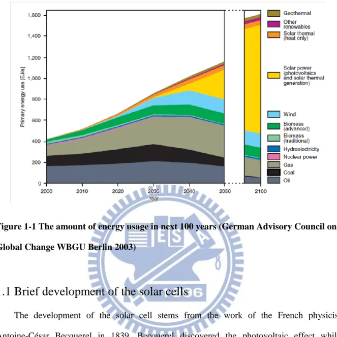
In this regard, an energy revolution can be expected, and the rise of green energy will play a big lead of the energy revolution. The green energy is a reusable and less polluting energy sources, such as wind, solar, geothermal, tidal, etc. Solar energy has a very large number of sources of supply. Because the sun produces about 1.76 × 10⁵ MW energy per year, of which 600 MW irradiation on the surface of the earth are available. Its energy is 100,000 times than the global average power. With technological advances, our solar energy use efficiency is also increased. It is expected for a large proportion in the next available energy sources account. From Figure 1.1, we can see the future of solar energy usage is expected to continue to rise.
2
Figure 1-1 The amount of energy usage in next 100 years (German Advisory Council on Global Change WBGU Berlin 2003)
1.1 Brief development of the solar cells
The development of the solar cell stems from the work of the French physicist Antoine-César Becquerel in 1839. Becquerel discovered the photovoltaic effect while experimenting with a solid electrode in an electrolyte solution. About 50 years later, Charles Fritts constructed the first true solar cells using junctions formed by coating the semiconductor selenium with an ultrathin, nearly transparent, layer of gold. But transform of Fritts's devices less than 1 percent of the absorbed light into electrical energy.
By 1927 another metal-semiconductor-junction solar cell, in this case made of copper and the semiconductor copper oxide, had been demonstrated. By the 1930s both the selenium cell and the copper oxide cell were being employed in light-sensitive devices, such as photometers, for use in photography. These early solar cells, however, still had
3
energy-conversion efficiencies of less than 1 percent. Finally, the silicon solar cell was been achieve development by Russell Ohl in 1941.
In 1954, three other American researchers, G.L. Pearson, Daryl Chapin, and Calvin Fuller, demonstrated a silicon solar cell capable of a 6-percent energy-conversion efficiency when used in direct sunlight. By the late 1980s silicon cells, as well as those made of gallium arsenide, with efficiencies of more than 20 percent had been fabricated. In 1989 a concentrator solar cell, a type of device in which sunlight is concentrated onto the cell surface by means of lenses, achieved an efficiency of 37 percent due to the increased intensity of the collected energy. In general, solar cells of widely varying efficiencies and cost are now available [3].
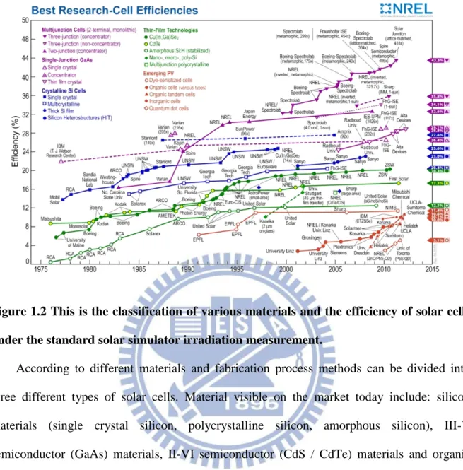
After the oil crisis, the most of the world’s countries alerted the important of new alternative energy development. The sun is just inexhaustible natural energy, neither energy depletion concerns, but also avoids the problem of energy monopoly. Therefore, countries actively developed the application of solar energy technology, expected by increasing the use of solar energy to reduce dependence on primary energy. The solar cell conversion efficiency research began to flourish. Today's market-oriented solar cells can be focus on the conversion efficiency of about range of 10% to 36% [4], while the theoretical maximum efficiency can reach 86% [5]. It can be seen that in the photoelectric conversion efficiency we have a lot of space to develop these technologies which will be a great help to solve the international community energy crisis in the future.
4
Figure 1.2 This is the classification of various materials and the efficiency of solar cells under the standard solar simulator irradiation measurement.
According to different materials and fabrication process methods can be divided into three different types of solar cells. Material visible on the market today include: silicon materials (single crystal silicon, polycrystalline silicon, amorphous silicon), III-V semiconductor (GaAs) materials, II-VI semiconductor (CdS / CdTe) materials and organic materials (TiO2) and etc. Figure 1.2 is the current solar cell material types and their efficiency
comparison chart. The GaAs solar cells is highest for the current efficiency, its efficiency can be as high as 30% or more, but it is expensive and containing highly toxic. In the early, it is used on the defense industry and space satellites, most recently the III-V semiconductor (GaAs) materials has been used to people’s livelihood for the high-efficiency concentrator solar power system. However, the organic solar cells are used in the commercial market yet, but it is really the direction of study at domestic and international. Although the photoelectric conversion efficiency of organic solar cells is currently low, but the process is simple, low cost, and has advantages of transmittance, large area manufacturing and can combine with the
5
flexible substrate. CIGS solar cell with low cost, long life and high efficiency potential is a lot of companies to invest in emerging industries, but there is no standardization of products and technical specifications. The CIGS solar cells used the indium material to fabricate. According to scholar’s statistic, the indium material left about 10,000 tons in the whole world. The next problem that CIGS solar cell has to face is lack of material in the future. Silicon solar cell technology is currently the most mature and widely applied. There are three types of silicon solar cells, including single-crystal silicon, polycrystalline silicon, and amorphous silicon solar cells. And single-crystal silicon and polycrystalline silicon solar cells are technically more mature and can be mass production.
1.2 The advantages and the challenge of a-Si thin film solar cells
The advantages of amorphous silicon solar cells fabricated by Carlson and Wronski are: The technology involved is relatively simple and inexpensive compared to the
technologies for growing crystals.
The optical properties of amorphous silicon are very promising for collecting solar energy
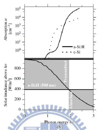
In Figure 1.3, the upper panel shows the spectrum for the optical absorption coefficients α(hν) for amorphous silicon and for crystalline silicon [6]. In the lower panel of the figure, we show the spectrum of the “integrated solar irradiance;” this is the intensity (in W/m2) of the solar energy carried by photons above an energy threshold hν [7].
6
Figure 1.3 (Upper panel) Spectra of the optical absorption coefficient α(hν) as a function of photon energy hν for crystalline silicon (c-Si) and for hydrogenated amorphous silicon (a-Si:H). (Lower panel) The solid curve indicates the irradiance of photons in the solar spectrum with energies hν or larger.
In this example, the figures used of a-Si:H and thin-layer thickness d = 500nm. Such a layer with the absorption of the photon's energy is basically greater than 1.9 eV. We assume the reflection of sunlight has been minimized and solar radiation can be found in the marked gray area of the absorption layer base to absorb the energy transfer of about 420 W/m2. The results of absorption in 500 nm thick layer of crystalline silicon less than 200 W/m2. In order to achieve 500nm a-Si: H thin layer of the same energy absorption as c-Si must be thicker. This means that the solar cells produced by the a-Si and c-Si is relatively only a very few materials.
But amorphous semiconductors contain intrinsic defects which increases the density of traps and recombination centers. For solar cells, this has the consequence that:
7
Diffusion lengths are shorter, so the material needs to be a strong optical absorber. Alternatively, multiple junctions must be used to make the device optically thick. In the case of very short diffusion lengths, it may be necessary to use extended built-in electric field to aid carrier collection. This is the case in amorphous silicon, where p-i-n structures are preferred.
Losses in the layers close to the front surface are greater, so it is advantageous to replace the emitter with a wider band gap window material.
The presence of defect states in the band gap can make the materials difficult to dope, and limit the built-in bias available from a junction through Fermi level pinning.
The presence of grain boundaries and other intrinsic defects increases the resistivity of the film particularly at low doping densities, and males the conductivity dependent on the carrier density, so influencing the electrical characteristics of devices.
The presence of defects similarly means that minority carrier lifetime and diffusion constant are carrier density dependent.
Good thin film materials should be low cost, non-toxic, robust, and stable [8]. They should absorb light more strongly than silicon. Higher absorption reduces the cell thickness and relaxes the requirement for long minority-carrier diffusion lengths, allowing less pure polycrystalline or amorphous materials to be used. Figure 1.4 compares the absorption coefficients for several photovoltaic materials and the maximum photo current which can be generated in a thin film as a function of its thickness. Notice how weakly crystalline silicon absorbs, in comparison with the other materials. Suitable materials should transport charge efficiently, and should be readily doped. Materials are particularly attractive if they can be deposited in such a way that arrays of interconnected cells can be produced at once (Figure. 1.4). This greatly reduces the module cost.
8
Figure 1.4 (a) Absorption coefficients of a number of different photovoltaic materials. (A derivative of the organic semiconductor polyphenylene vinylene (MDMO-PPV) is included for comparison.); (b) Maximum photon current available from each material under AM1.5 illumination, as a function of film thickness, assuming perfect collection of all photogenerated charges. The saturation photocurrent is a function of band gap. The maximum photocurrent supplied by the Am1.5 spectrum is around 49 mA/cm2. [9]
9
The future solar cell are as following, thin film, low-cost, high efficiency, so the amorphous silicon (a-Si) thin film solar cell was considered for future generation of photovoltaics applications. It can also be deposited on flexible substrate for versatile applications. Large area modules of a-Si solar cells have been widely commercialized. It can reduce the cost of fabrication process. However, a-Si thin film solar cells don’t have enough optical paths for incident light, but increase active layer due to poor carrier diffusion property and increase the cost. Therefore, we design adding anti-reflective and scattering structure, we attend to solve these problems and improve the efficiency of thin film solar cell.
So we want to use anti-reflection (AR) and light scattering structure in our design. Using AR coating can reduce reflection of sunlight, increasing the photons that enter the active layer to be absorption. In other hand, the light scattering structure increases optical length by changing the direction of incident-light-propagation, and also traps photons in the active layer by total reflection.
In this study, we have designed a photonic crystal structure. Due to the periodic change in refractive index with period ranging over lengths close to optical wavelength, anti-reflection and light scattering can be achieved. In addition, the photonic crystal layer was designed with a flat surface in order to avoid the decrease in Voc and F.F. caused by a rather
10
Chapter 2. The physics of a-Si thin film solar cells
2.1 The physics of solar cells
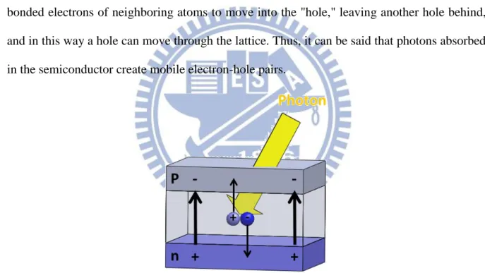
When a photon is absorbed, its energy is given to an electron in the crystal lattice. Usually this electron is in the valence band, and is tightly bound in covalent bonds between neighboring atoms, and hence unable to move far. The energy given to it by the photon "excites" it into the conduction band, where it is free to move around within the semiconductor. The covalent bond that the electron was previously a part of now has one fewer electron — this is known as a hole. The presence of a missing covalent bond allows the bonded electrons of neighboring atoms to move into the "hole," leaving another hole behind, and in this way a hole can move through the lattice. Thus, it can be said that photons absorbed in the semiconductor create mobile electron-hole pairs.
Figure 2.1 In a pn photodiode, excess electrons are donated from the n-type to the p-type layers, leaving the charges and electric fields illustrated. Each photon absorbed in the undoped, intrinsic layer generates an electron and a hole photocarrier. The electric field causes these carriers to drift in the directions shown.
A photon need only have greater energy than that of the band gap in order to excite an electron from the valence band into the conduction band. However, the solar frequency spectrum approximates a black body spectrum at about 5,800 K,[10] and as such, much of the solar radiation reaching the Earth is composed of photons with energies greater than the band
11
gap of silicon. These higher energy photons will be absorbed by the solar cell, but the difference in energy between these photons and the silicon band gap is converted into heat (via lattice vibrations — called phonons) rather than into usable electrical energy.
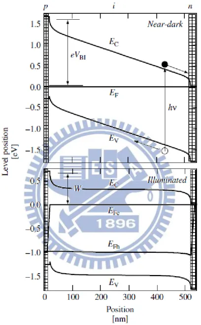
Figure 2.2 Bandedge and Fermi-level profiles in a pin solar cell under open-circuit conditions. The open-circuit voltage is precisely the value of EFh at the left interface (x =
0). The built-in potential VBI is illustrated. Note that the p-layer has a slightly (0.2 eV)
larger band gap than the i-layer; the calculation assumes symmetrical offsets of the valence and conduction bands at the p/i interface
12
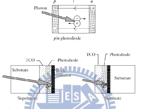
Figure. 2.3 shows the efficiency of amorphous silicon solar cell in the past 25 years. The basic concept of the three high-efficiency device: (1) PIN photodiode structure, (2) substrate and superstrate design, (3) multi-junction photodiode structure.
Figure 2.3 In a pin photodiode, excess electrons are donated from the n-type to the p-type layers, leaving the charges and electric fields illustrated. Each photon absorbed in the intrinsic layer generates an electron and a hole photocarrier. The electric field
causes these carriers to drift in the directions shown. pin diodes are incorporated into solar cells in either the superstrate or substrate designs. For amorphous silicon-based cells, photons invariably enter through the p-type window layer as shown here. [11]
The deposition of amorphous silicon solar cells have three layers deposited in either the p-i-n or the n-i-p sequence. The three layers are very thin (typically 20nm) p-type layer, a much thicker (typically a few hundred nanometers) undoped intrinsic layer (i-layer), as well as a very thin n-type layer. In this structure, excess electrons from the n-type layer toward the p-type layer, the positive charge and negative charge separation, creating a huge ‘built-in” electric field (usually more than 104 V/cm).
Sunlight enters the photodiodes as a flux of photons that pass through the p-type layer. p-type layer as almost transparent window layer. Solar photons mostly are absorbed in the much thicker intrinsic layer. The absorption of each photon will generate an electron and a
13
hole [12, 13]. By the built-in electric field separates the photocarriers to n-type layer and p-type layer, resulting in solar power.
Doped a-Si minority carrier mobile is not very far, only a p-n structure will collect the photogenerated carriers from the photon to produce a very thin layer of doped a-Si. In fact, in the analytical performance of a-Si solar cell, one normally considers any photons absorbed by the doped layers to be “wasted.” know-how to keep the doping atomic absorption layers of this layer is to make thick enough to capture the most sunlight.
One of the advantages of a-Si thin film solar cells is the ability to absorb sunlight very effectively, but the total absorption layer thickness is less than 1 micron. Therefore, these layers must have a thicker substrate support. Two totally different designs for amorphous silicon solar cells have evolved corresponding to transparent and opaque substrates. Show in Figure 2.3. In the “superstrate” design, sunlight enters through the transparent substrate, which is usually glass or a transparent plastic. The insulating substrate needs a conductive layer; which is typically transparent conductive oxide (TCO) such as tin dioxide (TiO2). The
amorphous silicon photodiode are deposited onto the TCO, start with a p-type window layer deposition. Finally, a back-reflection layer deposited onto the photodiode to act as an electrode to the n-type photodiode layer.
In the “substrate” design, the order of the sunlight enters the superstrate design compared to the opposite. The reflection fabricated on the substrate, followed by deposition of a photodiode and finally a TCO at the top layer as the electrode.
These two designs permit a very wide range of applications of amorphous silicon solar cells. The superstrate design (light enters through the substrate) is particularly suited to building-integrated solar cells in which a glass substrate can be used as an architectural element. The substrate design has generally been applied to solar cells using flexible, stainless steel (SS) substrates. The detailed construction of a deposition facility of course depends upon
14
whether the substrate is rigid or flexible. Finally, it turns out that there is a profound effect of the substrate upon the properties of the first photodiode layers deposited upon it; this effect has led to fairly different photodiode structures for the superstrate and substrate designs.
2.3 Introduction of a-Si thin film solar cells [11]
2.3.1 Brief history of a-Si
There are also many noncrystalline semiconductors. In these materials the chemical bonding of atoms is nearly unchanged from that of crystals. Nevertheless, a fairly small, disorderly variation in the angles between bonds eliminates the regular lattice structure. Such noncrystalline semiconductors can have fairly well electronic properties-sufficient for many applications. The first commercially important example was xerography in 1960s [14, 15]. Sterling and Swann exploited the photoconductivity of noncrystalline selenium. Selenium absorbs those photons from an incident light beam that have photon energies exceeding some threshold energy. The photon that is absorbed generates a positively charged “hole” and a negatively charged electron that are separated and swept away by the large electric fields used in x glow discharge.
However, solar cells require that photogenerated electrons and holes be separated by relatively modest electric fields that are “built-in” to the device. Selenium and many other noncrystalline semiconductors proved unsuitable for making efficient cells.
Around 1973, Walter Spear and Peter LeComber in Dundee, Scotland discovered that amorphous silicon prepared using a “glow discharge” in silane (SiH4) gas had unusually good
electronic properties. Its basis by Chittick, Sterling and Alexander established at an early stage [16]. Spear and LeComber in 1975, the electrical conductivity of amorphous silicon by mixing silane and phosphine (PH3) gas or some diborane (the B2H6) gas to increase. Like such
15
conductivity (n-type) and boron doping to enhance hole conduction (p-type).
In 1974, at the Radio Corporation of America (RCA) Research Laboratory in Princeton, David Carlson discovered that he could take advantage by using the silane glow discharge deposition to make the fairly efficient of thin films solar cells. In 1976, he and Christopher Wronski published an amorphous silicon based solar cell [17] conversion efficiency of about 2.4% [18, 19].
Carlson and Wronski amorphous silicon battery output voltage and current density in Figure 2.4. The scientists found that amorphous silicon thin films made by glow discharge (or “plasma deposition”) are very much superior to the amorphous silicon thin films prepared, for example, by simple evaporation of silicon.
Figure 2.4 Current density versus voltage under solar illumination for a very early single-junction amorphous silicon solar cell (Carlson and Wronski [17]) and from a recent “triple-junction” cell (Yang, Banerjee, and Guha [20]). The stabilized efficiency of the triple-junction cell is 13.0%; the active area is 0.25 cm2 [11]
After several years of development, there has been containing a substantial proportion of hydrogen atoms combine to plasma deposition of amorphous silicon structure, and these
16
hydrogen atoms is essential in improving the electronic properties of plasma deposited materials [21]. Therefore, the amorphous silicon (a-Si) has been generally known as hydrogenated amorphous silicon (a-Si: H). In recent years, many researchers have used in the hydrogenation of the amorphous silicon, hydrogen-free amorphous silicon so far only a few people in the study.
2.3.2 The characteristics of a-Si 2.3.2.1 Atomic Structure
The basic structure of the silicon atoms and amorphous silicon is roughly the same: each silicon atom is covalently attached to four other silicon atoms are arranged as a tetrahedron. Different amorphous structure compared to the crystal structure, connected with each other has curved amorphous covalent bond, there will be more than atoms and stick them in the fourth key, forming a perfect amorphous structure, and has a “dangling bonds.” Amorphous structure achieve the same crystal silicon atom bond length and bond angle values alloys [22, 23], such as As2Se3, the formation of amorphous cooling liquid.
For hydrogenated amorphous silicon (a-Si: H) in the Si-H bonds to resolve this structural problem. Percentage less silicon atoms make silicon covalent bond neighbors only three silicon neighbors, the fourth covalent bond silicon hydrogen atoms. The two principal “phases” of hydrogen evidenced by proton magnetic resonance are termed the dilute and clustered phases [24]. Distance of about 1 nm in the dilute phase hydrogen atom between two or more hydrogen atoms adjacent in the clustered phase. Structure is shown in figure 2.5 (a). The density of hydrogen depends on the conditions under which the material is made.
2.3.2.2 Defects and Metastability
Although the basic structure of amorphous Figure 2.5 shows, but it is also an ideal chemical structure: each atom to form a normal number of chemical bonds (four silicon atoms
17
and one hydrogen atom). This structure largely determines the overall electronic and optical properties, however, many a-Si:H electronic properties is also strongly influenced by the chemical bond defects [25]. Of a-Si:H defect atomic structure has been extensively studied in the electron spin resonance.
Figure 2.5 (a) hydrogenated amorphous silicon model. The gray areas show that the silicon atoms; white ball represents hydrogen, indicating that the clustered and relatively isolated dilute configuration (b) the a-Si:H dangling bond density and hydrogen density relationship. Data from the deuterium and defect profiles (350◦C deuterium). The curve of Zafar and Schiff from analog. [11]
A dangling bond [26] structure is illustrated in Figure 2.5 Imagine hydrogen atoms from a dilute phase is removed, leaving the lower right corner of the corner of a single non-bonding electron (referred to as the dangling bonds). Real-world observations, with the heating of the a-Si:H caused an increase in hydrogen to remove the dangling bond density. A measurement of this relationship has been proposed, as shown in Figure 2.5 (b) [27, 28] below. Need to pay attention to the density of the dangling bonds are generally much lower than the loss of density of hydrogen; it is difficult to produce hydrogen in the clustered phase dangling bonds.
18
Figure 2.6 The density of defects (dangling bonds) in the light a-Si: H film under measurement by Park, Liu, and Wagner [11, 29].
The most important of the a-Si:H defect study did not focus on the relationship between the hydrogen defects, but the effect of the light irradiation. But in the high-intensity lighting, the defect density reaches a steady state of about 1017/cm3. This is a very important purpose of the engineering and commercial applications, said the long light of a-Si:H will reach a steady state.
Hydrogen atoms and the a-Si:H between defects in close contact to understand the defects in the conditions created. The idea of this condition is to provide the energy required for lighting by the dilute phase away from the hydrogen atom transfer, thus creating a dangling bond, and by the change of a-Si:H preparation conditions reduce the impact of this effect [30].
Steady state of a-Si:H cell and thin film has considerable temperature dependence. For example, Figure 2.7 shows that the module efficiency is greatly affected by the season and highest following the hottest day of. The measurement may be understood by considering that the stabilized condition is due to competition between two rates: the creation of metastable defects by light and a thermally activated process that anneals them away.
19
Figure 2.7 Seasonal variations in the average conversion efficiency (solid symbols) of an amorphous silicon triple-junction module [31], along with the daily mean temperature (open symbols) [11]
2.3.2.3 Electronic Density-of-states
Optical and electronic properties of semiconductor are the most important concept to understand the electronic density-of-states g(E). If a single electron is added to a solid, it may be viewed as occupying a well-defined state (or molecular “orbital”) at a particular energy level E. Within a range of energy ∆E, the number of such states per unit volume of the solid is g(E)∆E
Figure 2.8 shows the density of states in hydrogenated amorphous silicon as it has emerged primarily from measurements of electron photoemission [32, 33], optical absorption [34], and electron and hole drift mobilities [35].. In the dark at low temperatures, the energy below the Fermi level states are electronic, the Fermi energy level above the state bit is empty. Two energy bands are as follows: an occupied valence band (E <EV), with Si-Si and
20
Figure 2.8 In hydrogenated amorphous silicon electronic density of states g(E). The shaded areas indicate delocalized states in the bands; these band tail-like state exponential distributions. The middle band is a serious defect, such as suspension Si bond displayed about two-band peak of the EF. [11]
2.3.2.4 Bandtails, Bandedges, and Band gaps
Any semiconductor, crystalline or amorphous, must have such an energy gap. For a perfect crystal, the valence band and conduction band edge EV and EC can be well defined,
and the energy gap of Eg = EC - EV. Disordered semiconductors are the exponential
distribution with a tail (bandtail) distributed in the bandedge near. For the valence band, can be written as g (E) = gvexp [- (E-EV) / ΔEV]. The width ΔEV for the interpretation of optical
absorption experiments the exponential distribution, significant spectrum in Figure 1.4. For a-Si:H, typical ΔEV = 50 × 10-3 eV, ΔEV also been used to explain the hole in the electric field
of the slow drift (the hole mobility) [35, 36]. Guide width ΔEC in the best a-Si: H material is
much narrower, about 22×10-3eV, but significant increase in the amorphous silicon germanium alloy.
In view of the index bandtails the presence of the bandedge the value has been questioned. Most people think of the band edge is separate from the electronic orbital energy. The bandedges accordingly referred to as the conduction band and valence band edge.
21
However, the amorphous semiconductor not exist a fixed bandedges state density; it is difficult to determine some of the ambiguities. Amorphous silicon used in solar cells, with different energy gaps, the most common measurement method is the analysis of optical absorption coefficient α (hυ) = (A/hυ)(hυ−ET)2
. is similar to Figure 1.4; one typical analysis yields an “optical” or “Tauc” band gap ET. The proportionality constant A just a
proportionality constant [38].
The bandgap of a-Si:H is usually about 1.75eV, essentially alloy or carbon germanium deposition and the environment will result in changes. The definition of higher than the Tauc band gap photon energy absorption coefficient α, α = 3×10³/cm production value (denoted as E3.5). Finally, learned that the optical band gap estimated and real gap of Eg = EC - EV is a
difference. Internal photon measurement [39] of the energy gap of about greater than of Tauc can gap 50 to 100 meV.
2.3.2.5 Defects and Gap States
The observation bandtails defect levels between the different energy levels in undoped a-Si: H, these levels is due to the dangling bonds (“D-centers”) by electron spin resonance measurements. For example, the infrared absorption of photon energy around 1.2 eV, and optical separation process so that the transfer of electrons from the valence band into the conduction band to produce a defect, the infrared absorption coefficient is proportional to the D-center density over a range of at least a factor of 100 in the density [40].
The next need to be resolved is the appropriate level, as shown in Figure 2.7. Able to gap the three charge states (with + e, 0 and -e), resulting in two levels (0/+ and -/0 charge state). Rough estimate of the near-dark conditions, (-/0) 0.6 eV, below about undoped a-Si:H low defect density EC [41]. The (+/0) level lies about 0.3 eV below the (-/0) levels; the difference
22
Apparently actually different densities in a-Si:H change doping, may be different between the samples of the dark and illuminated state [43].
2.3.2.6 Doping
Doped layer is an integral solar cell. This is by intentionally doped, such as phosphorus, boron atom, to change the Fermi energy. However, in amorphous silicon, doped with work and compared to crystalline silicon is very different. For example, in crystalline silicon, phosphorus (P) has five valence electrons in the lattice instead of silicon atoms, four electrons to participate in the adjacent silicon atom bonded. The fifth free electrons occupy the bottom of the conduction band, so that the doped Fermi level to about this level.
In amorphous silicon, phosphorus atom has only three neighbors. This is actually a favorable chemical structure, because the phosphorus atom in the form usually only three bonds (p orbitals of the three valence electrons). The last two electrons in the s orbital is not involved in binding, and maintain close links P atom. This makes the occurrence of a more powerful combination of amorphous silicon than crystalline silicon, but the lack of a rigid array. In amorphous silicon, it is necessary to rearrange the silicon lattice and leave a number of silicon dangling bonds, so that the P atoms in this configuration. For this reason, most of the excess energy for the rearrangement is expected to get a better P doping.
Therefore, phosphorus doping is a paradox in amorphous silicon. Street for the first time in 1982 to solve this problem. He recognized that the formation of a positively charged at the same time, coordination P4+ and negatively charged dangling bonds D- can occur occasionally
bonding, rather than the ideal tripartite coordination. This theory led to two important consequences [44]. Inefficient Si doping, most of the dopant atom does not help to provide free electrons, this cannot improve so that the Fermi level. Second, each atom of phosphorus dopant does provide electronic, but to be silicon dangling bonds. These defects, the doping
23
level is far below the conduction band. Since the electron and hole is photovoltaic (PV) energy conversion essential, doping will not contribute to the solar cell photovoltaic generation.
2.3.2.7 Alloying and Optical Properties
By substantially changing the deposition conditions affect the structural and optical properties. For example, to change the substrate temperature or diluted silane plasma deposition, lead to changes in a-Si:H thin-film optical energy gap, these changes can be attributed to the micro-structural changes in thin films of hydrogen in the range of 1.6 to 1.8eV [45]. Even larger elements of the alloy changes, such as Ge, can have an impact, the alloy of germanium, carbon, oxygen and nitrogen by mixed silane (SiH4) gas, such as GeH4,
methane, oxygen, or NO2 and NH3. The resulting alloy has a very wide range of band gap
a-Si1-xGex:H as an example in Figure 2.8. Simplicity, these alloys usually refers to the use of
the apostrophe: the a-SiGe or a-Si1-xGex:H.
There has been some material proved to be useful. In particular, a-SiGe alloy energy gap down to about 1.45 eV as the solar cells absorb a layer of narrow bandgap, so that amorphous silicon allows increasing the absorption to lower photon energy [46]. Figure 2.9 (a) shows the spectral absorption coefficient α(hυ), and change the a-SiGe alloy atomic percentage x the energy gap relationship. These data have two features to attract attention. First, the slope of the differences within the scope of the entire energy gap unchanged (about 50 meV). Second, the high absorption coefficient of the photon energy from the minimum steady increase in the energy gap decreases, the symbol of a corresponding increase in defect density.
Figure 2.9 (b) shows the change of a-Si1-xGex: H optical bandgap of Ge-ratio x and with
atomic fraction h of hydrogen. The figure reflects experimental results for a-Si:H alloys of varying H-fraction [47] and for a-SiGe:H alloys for which both x and h were reported [48].
24
For constant fraction h, the band gap decreases about 0.7 eV as the Ge ratio x increases from 0 to 1. The band gap increases with atomic fraction of hydrogen h. Energy gap with Figure 2.9 (b) as a useful approximation, especially the atomic ratio of h is the hydrogen in the a-SiGe microstructure, resulting in the possibility of contour map quantitative deviation. In addition, there are also some of the materials as a useful representative of the absorbing layer. In particular, Ge ratio x up to about 0.5, the optical performance becomes very poor, these alloys are no longer applicable to the solar cell [48]. Similarly, only a limited range of H atomic ratio of h yield useful absorption layer.
Figure2.9 (a) Absorption coefficient spectra for a-SiGe alloys; the optical band gaps and corresponding Ge fractions x are 1.25 to 0.58, 1.34 to 0.48, 1.50 to 0.30, 1.72 to 0.0 [45]. (b) Typical optical band gaps for a-Si1−xGex:H alloys for varying Ge-ratio x and atomic
fraction h of hydrogen. [11]
It might be thought that a-SiC is also applied to a wider range of bandgap absorption [49]. The widespread uses of B-doped a-SiC alloy material for the p-type window layer [50]. a-SiO and a-SiN is used as the insulator thin film transistor [51], but not the main solar modules.
25
Chapter 3. Simulation Method: RCWA
Figure 3.1 Geometry for planar-grating diffraction
The Rigorous Coupled-Wave Analysis (RCWA) is a method to compute diffraction of a field by a given grating structure [52-56]. Therefore the electric field will have only one component (in the y direction of Figure. 3.1). The relative permittivity in the modulated region (0 < z < d) is
where ε2 is the average dielectric constant, ∆ε is the amplitude of the sinusoidal relative
permittivity, ϕ is the grating slant angle, and K = 2π/Λ, where Λ is the grating period. The dielectric constant in the unmodulated regions (z < 0 and z > d) is ε1 and ε3, respectively. It is
assumed that each of the three regions has the permeability of free space.
The general approach to the planar-grating problem involves finding a solution of the wave equation in each of the three regions and then matching the tangential electric and (3-1)
26
magnetic fields at the two interfaces (z = 0 and z = d) to determine the unknown constants (resulting from solving the differential-wave equation). In region 1, backward-diffracted waves exist. In general, these waves are produced both by diffraction from within the grating volume (bulk diffraction) and by diffraction from the periodic boundary at z = 0 (boundary diffraction).
These diffraction processes produce spectrum of plane waves traveling back into region 1 (z < 0). The normalized wave amplitudes in region 1 may be expressed as [57-59]
where βi= k1sinθ - iKsinϕ for any integer i (the wave index); ξli2= kl2 - βi2 for l = 1, 3 (the region index); kl = 2πε1/2/λ for l = 1, 2, 3; λ is the free-space wavelength; j = (-1)1/2; θ is the angle of incidence in region 1; and Ri is the normalized amplitude of the ith reflected wave and is to be determined from the matching of the electric and magnetic fields.
In region 3 (z > d), the spectrum of transmitted plane waves may be expressed as
where Ti is the normalized amplitude of the ith transmitted wave to be determined from the field matching.
In region 2 (0 < z < d), the electric field may be expressed as
where ξ2i = k2cosθ' - iKcosθ, θ' is the angle of refraction inside the modulated region, and Ŝi (z)
is the normalized amplitude of the ith wave field at any point within the modulated region. For a given value of i, the wave field inside the grating is not a simple plane wave. It may be expressed as a superposition of an infinite number of plane waves (inherent in the coupled-wave formulation). This superposition includes forward-traveling waves (3-2)
(3-3)
27
(components in +z direction) and corresponding backward-traveling waves (components in -z direction). These amplitudes are to be determined from solving the modulated-region wave equation
To find Ŝi(z), Eqs. (3-1) and (3-4) are substituted into Eq. (3-5) with (ϕ = 0) resulting in the system of coupled-wave equations with Si (u) = Ŝi(z)
where ρ = 2λ2/(Λ2∆ε) = 2μ2ε2/∆ε, B = 2Λε21/ 2 cos (ϕ-θ')/λ, and u = jπ∆εz/(2λε21/2cos (ϕ-θ')) =
jγ(z/d). Here B is the Bragg condition parameter, which is unity for first Bragg incidence. The quantity ρ is the regime parameter, which is shown in this article to determine the boundary for the two-wave Bragg diffraction regime (ρ>10) for reflection gratings. Thus, this parameter is shown to have significance for reflection gratings similar to its significance in transmission gratings.
Equation (3-6) can be written in matrix “state equation” form as
where S, S', and S" are the column vectors Si(u), dSi(u)/du, and d2Si(u)/du2, respectively, and [brs] is the coefficient matrix determined from Eq. (3-6). The solution of Eq. (3-7) gives the
field amplitude Si(u) as
where q are the eigenvalues of the matrix [ω] composed by the eigenvectors of the coefficient matrix [b]. Note that ωim is the mth element of the row of the matrix [ω] that corresponds to the ith wave (not the ith row). The coefficients Cm together with Ti and Ri are determined by matching the tangential electric and magnetic fields at the two boundaries (z=0 amd z=d). The (3-5)
(3-6)
(3-7)
28 boundary conditions give
where δi0 is the Kronecker delta function and
In regions 1 and 3, ξli is either positive real (propagating wave) or negative imaginary (evanescent wave). The system of linear equations given by Eqs. (3-9) and (3-10) can be solved for Cm, and then Ri and Ti.
when tangential electric field at z = 0:
tangential magnetic field at z = 0:
tangential electric field at z = d:
tangential magnetic field at z = d:
Note that the number of equations available is exactly equal to the number of unknowns. For example, if n waves are retained in the analysis, then there will be n unknown values each of Ri and of Ti and 2n unknown values of Cm. This is because the coefficient matrix [b] in Eq. (3-7) is a 2n × 2n matrix and therefore has 2n eigenvalues, and thus there are 2n unknown values of Cm. Alternatively, this may be viewed as being due to the n coupled-wave equations, (3-11) (3-12) (3-13) (3-14) (3-15) (3-16) (3-10) (3-9)
29
each being a second-order differential equation, and thus there are 2n roots or eigenvalues and 2n unknown constants Cm to be determined from the boundary conditions. Therefore the total number of unknowns is 4n, and Eqs. (3-13)~(3-16) provide 4n linear equations in these unknowns.
To summarize, the algorithm used to solve this problem proceeds as follows: First the coefficient matrix [b] is constructed, and then eigenvalues and eigenvectors are calculated (typically by using a computer library program). The system of linear equations, Eqs. (9) and (10), is then constructed and solved for Cm (using a technique such as gauss elimination). Equations (13) and (14) are then used to calculate the diffracted amplitudes Ri and Ti. Power conservation requires that the sum of the efficiencies for all of the propagating waves be unity. That is,
where DE1i and DE3i are the diffraction efficiencies in regions 1 and 3, respectively. These diffraction efficiencies are given by
and
The real part of the ratio of the propagation constants occurs when the time-average power-flow density is obtained by taking the real part of the complex Poynting vector. The quantity Re(ξli/ξ10) is just the usual ratio of the cosine of the diffraction angle for the ith wave to the cosine of the angle of the 0th-order wave for the lth medium. The results a function of the grating strength parameter γ (= κd/cos θ') and as a function of d/Λ for a pure transmission grating (ϕ = π/2), for general slanted gratings (ϕ = π/3, π/6), and for a pure reflection grating (ϕ = 0).
(3-17)
(3-18)
30
Chapter 4. Light Management
4.1 Light trapping
Light confinement increase the fraction of photons admitted to the cell, and concentration which increase the incident flux, light confinement techniques increase the path length of photons inside the cell. Increasing the path length increases the probability of photogeneration per incident photon, particularly when the absorption coefficient is small, increasing the absorbed fraction. Light trapping is normally considered in the regime of geometrical optics where structures are large compared to the coherence length of the light, and light rays with different history do not interfere. This is a good approximation in silicon where cells are hundreds of microns thick. In micron scale structures, light should be treated as coherent and interference becomes important. In such systems, classical ray tracing approaches are not valid, and the photogeneration rate must be found from the gradient of the Poynting vector.
The simplest light trapping scheme is to introduce an optical mirror at the rear surface of the cell, either by metallizing the rear cell surface or by growing the active layers on top of a Bragg grating structure. The mirror typically reflects over 95% of rays striking the rear surface. Reflective light subsequently reach the front, semiconductor-air, surface are likely to pass through since the reflectivity of that interface must be small for efficient light capture. So the rear mirror effectively doubles the path length of the light. For an ideal mirror (with R = 1) and ideal front surface (with R = 0) the path length is 2w.
The simplest is where one surface is tilted relative to the other. Consider a rear surface tilted at an angle θtilt relative to the planar front surface, as in Figure 4.1. When θtilt > θc,
normally incident rays will be reflected from the rear surface at an angle greater than θc, and
31
second pass, it will be reflected at an even wider angle, and trapped again. For uniform cell width, both positive and negative tilt angles must be present, so that trapped rays will eventually be reflected at narrower angles and escape. If the positive and negative tilt angles are equal, then each ray makes a multiple of four passes across the cell.
Figure 4.1 Light trapping structures with a tilted rear surface, illustrating a “double bounce” light path [60].
4.2 Reflection
The optical properties of a solid are described by the dielectric constant, εs. εs is a
complex quality and obeys
where ns in the refractive index of the material and the imaginary part ks is related to the
absorption coefficient of the material through
In general, εs, ns and ks are wavelength dependent, and may be direction dependent.
Differences in refractive index determine the reflection and transmission of light at the interface between two materials. For thin films, light should be treated as coherent, and Maxwell’s equations can be solved to find the relative amplitudes of transmitted and reflected waves. In the simplest case, that of a plane boundary between materials of refractive index n0 and ns, light striking the interface at normal incidence is reflected with probability
(4-1)
(4-2)
32
For a semiconductor, ns is typically 3~4 at visible wavelengths (Table 4.1), so that some
30~40% of light normally incident on the surface from free space will be reflected.
Table 4.1 Refractive indices of selected semiconductors and AR coat materials.
At oblique incidence the reflectivity is angle and polarization dependent. If the incident ray makes an angle θ0 with the surface normal, and the transmitted ray an angle θs with the
surface normal inside the semiconductor then
where
for p polarized light (with the electric field vector in the plane of incidence and
and for s-polarized light (electric field vector normal to the plane of incidence). θ0 and θs
are related through Snell’s law
For unpolarized light, considered as an equal mix of s and p polarizations, the net reflectivity generally increases with angle (for the s polarized component it increase while for (4-4)
(4-5)
(4-6)

![Figure 2.4 Current density versus voltage under solar illumination for a very early single-junction amorphous silicon solar cell (Carlson and Wronski [17]) and from a recent “triple-junction” cell (Yang, Banerjee, and Guha [20])](https://thumb-ap.123doks.com/thumbv2/9libinfo/8734502.202459/29.892.212.700.474.932/current-illumination-junction-amorphous-carlson-wronski-junction-banerjee.webp)
![Figure 2.6 The density of defects (dangling bonds) in the light a-Si: H film under measurement by Park, Liu, and Wagner [11, 29]](https://thumb-ap.123doks.com/thumbv2/9libinfo/8734502.202459/32.892.233.724.121.337/figure-density-defects-dangling-bonds-light-measurement-wagner.webp)
![Figure 2.7 Seasonal variations in the average conversion efficiency (solid symbols) of an amorphous silicon triple-junction module [31], along with the daily mean temperature (open symbols) [11]](https://thumb-ap.123doks.com/thumbv2/9libinfo/8734502.202459/33.892.217.733.109.473/figure-seasonal-variations-conversion-efficiency-amorphous-junction-temperature.webp)
