金氧半導體元件雜訊對射頻積體電路的影響
97
0
0
全文
(2) 金氧半導體元件雜訊對射頻積體電路的影響. Impacts of Noise on the CMOS RF Integrated Circuits 研究生:許孟庭. Student: Meng-Ting Hsu. 指導教授:高曜煌 博士. Advisor: Dr. Yao-Huang Kao. 國立交通大學 電信工程學系 博士論文 A Dissertation Submitted to the Institute of Communication College of National Chiao Tung University In Partial Fulfillment of the Requirements For the Degree of Doctor of Philosophy In Communication Engineering June 2004 Hsinchu, Taiwan, Republic of China. 中華民國 九十三 年 九 月.
(3) 金氧半導體元件雜訊對射頻積體電路 的影響 研究生:許孟庭. 指導教授:高曜煌 博士. 國立交通大學電信工程學系博士班. 摘要 本論文的目標在研究元件的雜訊在射頻電路設計中的角色。對低 雜訊放大器而言,描述在不同的頻率範圍下,具有源極迴授式之低雜 訊放大器技術已被印證其可行性。經由兩種不同的方法了解雜訊與輸 入阻抗之變化情形,首先經由雙埠網路觀察最小雜訊指數和等效輸入 電阻隨源極電感而產生的變化。其次,經由等效模型萃取出影響最小 雜訊指數和等效輸入電阻之主要元素,在 C 頻段下使用此技術,可同 時獲得具有負 23 分貝的優良輸入反射損失和 1 分貝的最小雜訊指 數。封裝元件應用在此源極電感迴授式之頻率限制亦同時著墨。其 次,使用聯電 0.5um 金氧半導體技術製作積體化低雜訊放大器,在偏 壓 3 伏特和操作頻率 2.4GHz 下,信號增益 12.5dB ,雜訊指數 5.6dB 和 40mW 的消耗功率。由於閘極電阻率較高,使得雜訊指數及訊號增 益量明顯受到影響,因此在設計射頻積體電路晶片製作上需考慮低閘 極電阻率之製程參數,提升電路操作性能。 另外,使用台積電 0.35um 金氧半導體技術製作積體化壓控振盪. i.
(4) 器亦被提出,他具有 2GHz 的振盪頻率,在 3 伏特偏壓下功率消耗為 23.58mW 且有 9.1%頻寬調制。在晶片製作中,最佳化電感佈局設計不 僅提升品質因素,更降低了相位雜訊。文中亦提出預測相位雜訊的計 算法,經由量測結果得到在 600KHz 的偏移頻率下,其相位雜訊為 -115.5 dBc/Hz。依觀察,預測數值與量測數據相當吻合。. ii.
(5) Impacts of Noise on the CMOS RF Integrated Circuits. Student: Meng-Ting Hsu. Advisor: Dr. Yao-Huang Kao. Institute of Communication National Chiao Tung University. Abtract The goal of this thesis is to study the noise phenomenon and property of the device. And how noise applied to design the RF circuits. First, the noise figure to LNA is presented. The feasibility of the technique of source inductive feedback (SIF) for low noise amplifiers (LNA) design is examined in different frequency domains. The variations in noise and input impedance are obtained by two different approaches. One is from a noisy two-port analysis to observe the variation of Fmin and Rn , and the other is from equivalent circuit model to trace out the key element. Using ISF, the results with both good input return loss about -23dB and low minimum noise figure about 1dB at C band are demonstrated. The frequency limitations of the SIF technique in package devices are also addressed.Another circuit of 2.4GHz CMOS LNA was fabricated by the process of UMC 0.5um DPDM technology. It has 12.5dB gain and 5.6dB noise figure under 3V bias. Owing to the gate sheet resistance 30 Ω / □ is so high that it affects the noise figure and signal gain. From the noise analysis of gate effect to LNA, it shows very match the noise level by taking gate resistance of the device into account. In words, choosing lower sheet resistance of poly gate is necessary to RF circuits. Secondly, the phase noise to VCO with 2GHz operating frequency is proposed. The fully integrated LC voltage controlled oscillator by TSMC 0.35um CMOS technology is demonstrated. It has 2GHz oscillation frequency, 23.58mW power consumption under 3V biased and 9.1% frequency tuning. The layout optimization iii.
(6) method of inductor to increase quality factor and also to reduce phase noise is used. A general method is proposed which is capable of making an effective prediction of F, device excess noise number, and acquiring to phase noise of oscillators accurately. From this proposed method, the low phase noise by calculation is attained. The phase noise of measured value which shows good match with calculating data is about -115.5dBc/Hz at offset frequency 600KHz.. iv.
(7) 誌謝 感謝上帝讓我有機會進入國立交通大學電信研究所接受微波電 路和射頻積體電路相關領域的訓練與磨練。更高興的是能夠受教於 高曜煌 教授的門下,一窺高頻電路和積體電路設計的堂奧。在七年 的寒暑交替中,品嚐到知識累積的可貴和價值,更學習了挑戰困難及 解決問題的正確態度與方法。雖然在整個學習過程中倍感艱辛、五味 雜陳,但每次困難得以解決,無形中能力隨之提昇,心中亦充滿著極 大的喜樂。另外也要特別感謝雲林科技大學電子系 周榮泉 教授常常 給予鼓勵與關懷,並於投稿文件中的指導與建議。 在這段漫長的學習過程中,光纖通訊和高頻電路實驗室給我寬廣 的成長空間,令人難忘,尤其是伴我奮鬥了好幾屆的學弟,再次重點 代表題名道謝,李柏榮、謝義濱、林哲煜、吳莊雄、李佳穎、莊朝喜、 游秋榮、林烱宏、柯勝民、許民傑、吳丕安、謝東憲、曾渾洸、曾耀 緯…等多位學弟彼此鼓勵和幫助,使得實驗室在這幾年間於射頻積體 電路領域中打響了知名度,這是本實驗室值得慶賀之處,本人能躬逢 其盛,亦倍感光榮。 我還要感謝國家晶片設計製作中心(CIC)提供晶片設計及製作的 優良環境,使得論文中積體電路設計之實驗應證得以順利完成。同時 亦感謝工研院和奈米元件實驗室在量測儀器上的支援,使得量測數據 的蒐集和整理能快速完成。此外,亦要感謝雲科大的專題生劉俊宏、 蔡嘉偉、金廷嶽、鄒宜勳和方浩宇在排版及校稿上之協助,使得博士 論文能夠順利完稿。 最後,我要感謝父母和家人付出的關懷和鼓勵,尤其岳父母在此 期間幫忙帶小孩,使我更專心於學習而無牽掛,相信沒有這些人的幫 忙與協助,就沒有今日的我。在此衷心地感謝伴我渡過七年寒暑的 人、事、物。. 許孟庭 書於 風城交大 九十三年九月初秋 v.
(8) Contents Chinese Abstract. i. English Abstract. iii. Acknowledges. .. Table of Content. v ..vi. List of Tables. ix. List of Figures. .x. Ch. 1. Introduction. ... 1. 1.1 Motivation ……..…………………………………………….…….…...1 1.2 Review of Receiver Design …….……….………………….……….5 1.3 Organization of This Thesis ……………………………...…………….9 Ch. 2. General Noise Theory. .11. 2.1 Introduction to Noise Concept ………………...……………………11 2.2 Type of Noise ………………………………...……………………..13 2.2.1 Thermal Noise ………………………..……………...……..14 2.2.2 Shot Noise ……………………………..………...…………14 2.2.3 Flicker Noise …………………………..………...…………15 2.3 Noise Models for Circuit Elements …………..…………………….16 2.4 Noise Theory Apply to RF Circuit ...…………..……………...…....20 2.4.1 Definition of Noise Figure by Two-Port Network ……...….20 2.4.2 Oscillator Phase Noise ……………………………........…..21 2.4.3 Lesson’s Model for Phase Noise ……………………….…..23. vi.
(9) Ch. 3 Microwave Low Noise Amplifier with Source Inductance Feedback. 26. 3.1. Introduction …………………………………...…………………..26. 3.2. Calculations of Noise Parameters …….………………...………….26 3.2.1. Low-Noise Amplifier Deisgn …..…………………………26. 3.2.2. Noise Two-port Network Theory of Cascode Connection.. 28. 3.2.3. Graph of Numerical Computation with Loci of Γopt. 3.2.4. *. and S11 …………………………………………… 32. Experiment of Both Input Impedance and Noise Matching …………………………………………...34. 3.3. Analysis From The Equivalent Circuit ……………………...……..35 3.3.1. Verification by small signal noise model ……..…………..35. 3.3.2. Discussion of Parasitic Effects on Frequency Performance ……………………………………………...37. 3.3.3 3.4. Ch.4. Conclusions...…………..………………………………….37. Noise Analysis of 2.4GHz CMOS LNA ……...…………..……38 3.4.1. Topology of Low Noise Amplifier …….……………...38. 3.4.2. Conventional Design Flow of LNA ...………….…………39. 3.4.3. Measurement and Discussion …………………...………...40. 3.4.4. Conclusions ………………………………………………43. Design of the CMOS Voltage-Controlled Oscillator. .44. 4.1. Introduction…..…….………………………………………………44. 4.2. Microwave Circuit Design of VCO ……….......……………….….46 4.2.1 One-Port Negative Resistance Microwave Oscillator ……..46 4.2.2 Two-Port Network of Microwave Oscillator ………..…49. vii.
(10) 4.3. Integrated Circuit Design of Complementary Cross-Couple pair VCO ………………………………………………………....51 4.3.1. On-Chip Spinal Inductor Design………………………... 52. 4.3.2. Frequency tuning by MOS Varactor ……………..…...55. 4.4. Simple Description VCO Circuit………………………………….57. 4.5. Prediction Method of Phase Noise ………………………...……...58 4.5.1. Prediction of Phase Noise ….…………………….…….58. 4.5.2. Phase Noise minimization …………….……………..…59. 4.6. Simulation and Measurement……………………………………..62. 4.7. Verification of VCO Design ..……………………………………65 4.7.1. Maximize the Oscillation Power ………...…………….65. 4.7.2. Prediction of Phase Noise on Frequency domain ….…..67. 4.7.3. Analysis of Phase Noise by linear time varying. ... method………………………………………………... 67 4.8 Ch.5. Conclusion ………………………………………………………75. Conclusion. .. 76 … 77. Reference. viii.
(11) List of Tables 1.1 Wireless System Frequencies ……………………………………………………2 1.2 Major Worldwide Cellular and PCS Telephone Systems ………………………..4 3.1 NEC NE42484A under Vds = 2V and Ids = 10mA ……………...……………....29 3.2 Small signal parameters included noise parameters ……………………………36 3.3 Design parameter of 0.5 um UMC DPDM technology ………….……...…40 4.1 Device size of cross-coupled pains VCO circuit ……………………………….62 4.2 The Summary of VCO performance …………………………………………....65 4.3 Extracted Value of Kf and α. of flicker noise.……………………………70. 4.4 Phase noise contribution of each part in the VCO circuit ……………………....74 4.5 Comparison with some reported papers basing on the same structure and related technology ……………………………………………………………...75. ix.
(12) List of Figures 1.1 Block diagram of a single-conversion superheterodyne receiver …………….... 6 1.2 Block diagram of a double-conversion superheterodyne receiver ………………7 1.3 Diagram illustrating the change in power levels between the input and output of a typical reveiver...………………………………………………………….....7 1.4 Diagram of power and noise levels at consecutive stages of receiver …………...8 2.1 Output of a generator and the sound of a river ....………………........................11 2.2 Average noise power .....………………………………………………...………12 2.3 Calculation of noise spectrum ...…………………….………………………......13 2.4 Thermal noise of a resistor...………………………………………………….....14 2.5 Flicker noise spectrum …………………………………………………………...15 2.6. Concept of flicker noise corner frequency……………………………………...16. 2.7. Circuit elements and their noise modes……………………….………………..17. 2.8 Opamp circuits showing the need for three noise source in an opamp noise model…..………………………………………………………………………..19 2.9. (a) Noisy two-port network; (b) noiseless two-port representation ……..……..20. 2.10. Output spectrum of ideal and actual oscillators …………………………........21. 2.11. Feedback amplifier model for characterizing oscillator phase noise…….........23. 2.12 .Noise power versus frequency for an amplifier with an applied input signal... ...24 2.13 .Idealized power spectral density of amplifier noise, including 1/f and thermal components…………………………………………………………... 25. x.
(13) 2.14 .Power spectral density of phase noise at the output of an oscillator. (a) response for (low Q). (b) response for (high Q) …………………….………..25 3.1 .Block diagram of the single stage microwave amplifier with SIF ...………....29 3.2. Loci of (a) Γopt , (b) S11* as functions of feedback inductor from 0 to 1nH at various frequencies with NE42484 biased at V ds=2V, Ids=10mA ………..…...33. 3.3. Behaviors of (a) Fmin and (b) RN. as functions of feedback inductor for. NE42484 biased at Vds=2V, Ids=10mA ………………...………………...…...33 3.4 . ..Experimental results of a C-band amplifier with SIF (a) low noise performance and (b) gain and return loss ……………………………...…......34 3.5. Equivalent small-signal model including the package effects and noise sources ………………………………………………………………………...35. 3.6. F min versus L for intrinsic model plus C gd , Rds and C ds individually for curve A, B, C respectively at frequency 18GHz ……………………….....36. 3.7. Fmin as a fucntion of inductance L in various value of package parasitic Cpg. from 0 pf to 0.2pf with 0.04 pf increase for each curve from curve 1 to curve 6 at 14 GHz...……………………………………………..…37 3.8. LNA whole circuit ………………………………………………………….…38. 3.9. Device geometry for particular power consumption and noise figure ………..39. 3.10 .Return loss S11 of LNA …………………………………………………….….40 3.11 .S21 of LNA…………………………………………………….…………….…41 3.12 .Input noise and gain matching curves. ....………………….………….....…...41. 3.13 .Measured S11 and those calculated with / without R g in the BSIM3V3 model…………………………………………….………..…….…42. xi.
(14) .3.14 .S21 measured and simulation results……………………….…………….…….43 4.1 The schematic of S35-90D VCO ……………………………………………...45 4.2. The photograph of S35-90D VCO …………………………………...……….45. 4.3 .Circuit for a one-port negative-resistance oscillator ………………………....46 4.4. Linear variation of the negative resistance as a function of the current amplitude …………………………………………………………….…...….48. 4.5 Two-port oscillator model …………………………………………………….49 4.6 LC complementary cross-coupled design procedure ……………..……...…...51 4.7 The simulation of the inductance and the Q factor..……………………....…..53 4.8. (a) Constant width spiral inductor ……………….…………………….....…..54. 4.8. (b) Optimum width spiral inductor …………………….………….…....…….54. 4.8. (c) Dummy pad for de-embedding ……..…………………………………….54. 4.9 The measured Q factor comparison between constant width and optimum width …………………………………………………………………....…..…54 4.10. Inversion-mode capacitor ………………………………………………........56. 4.11. Tuning characteristic for the p-MOS capacitor with D≡S≡B…………...…...56. 4.12. tuning characteristics of the p-MOS via Hspice simulation with D≡S, B=Vdd , W/L=400um/0.35um …………………….…………...….…56. 4.13. Illustration of positive feedback ……………………………………...……..57. 4.14. (a). gL. 4.14. (b). L2 g L vs. inductance …………………………………………...…...….59. vs. inductance ……………………………………………...……...59 2. 4.15 The spectrum with current injection at f m ………………………...………...61 4.16 The optimum situation with the lowest side band level …………...…………61 4.17 The phase noise measurement of the S35-90D VCO ……………...…………63 4.18 The measured VCO output spectrum ……………………………...…………64 xii.
(15) 4.19 The tuning range in terms of peak power holding of S35-90D VCO ..………..64 4.20 (a) Conceptual block diagram of the oscillator ………………………………..66 4.20 ..(b) Dependence of negative resistance on oscillation current at 2GHz …….…66 4.21 Blook diagram of linear time-varying analysis …………………………….….68 4.22. Measurement of NMOS flicker noise with different Vds under Vgs=1V..…....69. 4.23. Measurement of NMOS flicker noise with different Vgs under Vds=1V …....70. 4.24 MOSFET flicker noise ………………………………………………………...72 4.25 Impulse sensitivity function (ISF) of MOS current noise. ………………….…73 4.26 The calculated phase noise spectrum by linear time-varying model …………..74. xiii.
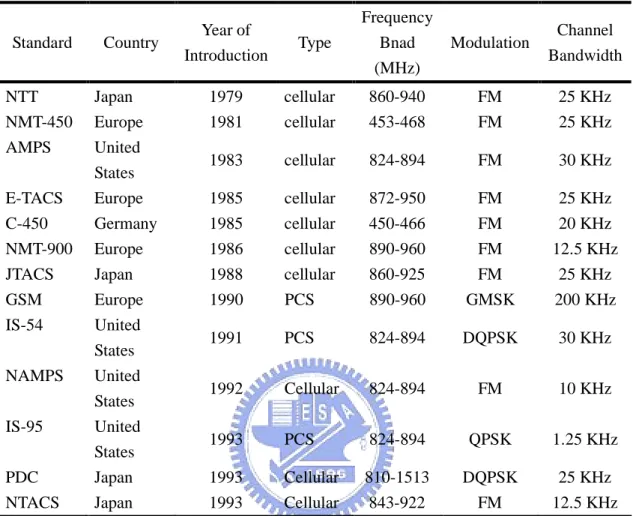
(16) Chapter 1 Introduction 1.1 Motivation In the early 1980s a marketing firm hired by AT&T to survey the potential U.S. market for its newly inaugurated cellular phone service arrived at an estimate of less than 900,000 users by the year 2000. Like many predictions of technological progress, this one turned out to be off by a wide margin—in 1998 the number of cellular subscribers in the United States was over 60million (already an error of more than 6000 percent). It is now estimate that half of all business and personal communications will be wireless by the year 2010 [1]. Rapid growth is also occurring with other wireless systems, such as Direct Broadcast Satellite (DBS) television service, Wireless Local Area Networks (WLANs), paging systems, Global Positioning Satellite (GPS) service, and Radio Frequency Identification (RFID) systems. These systems promise to provide, for the first time in history, worldwide connectivity for voice, video, and data communications. The successes of wireless technology to date, and the technological challenges of future wireless systems, make this an exciting and rewarding field in which to work. In this section we give a brief introduction to some of the major wireless systems in use today. These include wireless cellular and PCS telephone systems, wireless data networks. Wireless systems can be grouped according to their operating frequency. Table 1.1 lists the operating frequencies of some of the most common wireless systems. Cellular telephone systems were proposed in the 1970s in response to the problem of providing mobile radio service to a large number of users in urban areas. Early mobile radio systems could handle only a very limited number of users due to inefficient use of the radio spectrum and interference between users. In 1976, for example, the entire mobile phone system in New York City could support only 543 users [1]. The cellular radio concept introduced by Bell Laboratories solved this problem by dividing a geographical area into non-overlapping hexagonal cells, where each cell has its own transmitter and receiver (base station) to communicate with the mobile users operating in that cell. Each cell site may allow as many as several hundred users to simultaneously communicate with other mobile users, or through the land-based telephone system. The first cellular telephone system to offer commercial service was built by the Nippon Telephone and Telegraph company (NTT), and became operational in Japan 1.
(17) TABLE 1.1. Wireless System Frequencies. Wireless System. Operating Frequency. Advanced Mobile Phone Service (AMPS). T: 824-849 MHz R: 869-894 MHz. Global System Mobile (European GSM). T:800-915 MHz R:925-960 MHz. Personal Communications Service (PCS). T:1710-1785 MHz R:1805-1880 MHz. US Paging. 931-932 MHz. Global Positioning Satellite (GPS). L1:1575.42 MHz L2:1227.60 MHz. Direct Broadcast Satellite (DBS). 11.7-12.5 MHz. Wireless Local Area Networks (WLANs). 902-928 MHz 2.400-2.484 GHZ 5.725-5.850 GHz. Local Multipoint Distribution Service (LMDS) US Industrial, Medical, and Scientific bands (ISM). 28GHz 902-928 MHz 2.400-2.484 GHz 5.725-5.850 GHZ. T/R = mobile unit transmit/receive frequency in 1979. This was followed by the Nordic Mobile Telephone (NMT) system in Europe, which began operation in 1981. The first cellular telephone system in the United States was the Advanced Mobile Phone System (AMPS), deployed by AT&T in 1983. All of these systems use analog FM modulation and divide their allocated frequency bands into several hundred channels, each of which can support an individual telephone conversation. These early systems grew slowly at first, because of the initial costs of developing an infrastructure of base stations and the initial expense of handsets, but by the 1990s growth became phenomenal. In 1998 88% of all cellular telephones in the United States used the analog AMPS system, but newer digital standards have been growing in popularity and will 2.
(18) soon replace the AMPS system. These systems are generally referred to as Second Generation Cellular, or Personal Communication Systems (PCS). Third generation PCS systems, which may include capabilities for email and Internet access, are in the planning stages. Because of the rapidly growing consumer demand for wireless telephone device, as well as advances in wireless technology, several second generation standards have been proposed for improved service in the United States, Europe, and Japan. These PCS standards all employ digital modulation methods and provide better quality service and more efficient use of the radio spectrum than analog systems. Digital systems also provide more security, preventing eavesdropping through the possible use of encryption. PCS system in United States use either the IS-136 time division multiple access (TDMA) standard, the IS-95 code division multiple access (CDMA) standard, or the European Global System Mobile (GSM) system [1], [2], [3]. Many of the new PCS systems have been deployed using the same frequency bands as the AMPS system. This approach takes advantage of existing infrastructure, and facilitates the use of dual-mode handsets that can operate on both the older AMPS system as well as one of the newer digital PCS systems. Additional spectrum has also been allocated by the Federal Communications Commission (FCC) around 1.8GHz, and some of the newer PCS systems use this frequency band. Outside the United States, the Global System Mobile (GSM) TDMA system is the most widespread, being used in over 100 countries [1]. The uniformity of a single wireless telephone standard throughout Europe and much of Asia allows travelers to use a single handset throughout these regions. In contrast, the different PCS systems in the United States are incompatible. Table 1.2 lists the major cellular and PCS telephone systems that have been deployed throughout the world [1], [3]. It is interesting to compare how the development of first and second generation cellular services has differed in the United States and Europe [1]. The first U.S. cellular system, AMPS, provided a single standard allowing every cellular user in the United States and Canada to communicate within range of a base station. In the Europe of the early 1980s, however, individual countries developed their own analog cellular standards with different frequency bands and modulation methods, so that there were at least four incompatible systems in use (see Table 1.2). These situations were reversed for second generation digital systems. The organization of European countries under the European Union in the 1980s led to the establishment of GSM as a single digital PCS standard, which is now used by over 100 countries in Europe and elsewhere. In the United States, however, government policies relating to the allocation of radio spectrum, as well as the structure of the telecommunications 3.
(19) TABLE 1.2 Standard. Country. Major Worldwide Cellular and PCS Telephone Systems Year of Introduction. Type. Frequency Bnad (MHz). Modulation. Channel Bandwidth. NTT NMT-450 AMPS. Japan Europe United States. 1979 1981. cellular cellular. 860-940 453-468. FM FM. 25 KHz 25 KHz. 1983. cellular. 824-894. FM. 30 KHz. E-TACS C-450 NMT-900 JTACS GSM IS-54. Europe Germany Europe Japan Europe United States. 1985 1985 1986 1988 1990. cellular cellular cellular cellular PCS. 872-950 450-466 890-960 860-925 890-960. FM FM FM FM GMSK. 25 KHz 20 KHz 12.5 KHz 25 KHz 200 KHz. 1991. PCS. 824-894. DQPSK. 30 KHz. NAMPS. United States. 1992. Cellular. 824-894. FM. 10 KHz. IS-95. United States. 1993. PCS. 824-894. QPSK. 1.25 KHz. PDC NTACS. Japan Japan. 1993 1993. Cellular Cellular. 810-1513 843-922. DQPSK FM. 25 KHz 12.5 KHz. industry and the competitive nature of R&D in the United States, has allowed the technological and economic trade-offs between CDMA, TDMA, and GSM PCS systems to be decided in the marketplace. Meanwhile, wireless telephone consumers in the United States are left to choose between an out-of-date analog system and a variety of incompatible digital systems. Wireless local area networks (WLANs) provide connections between computers over short distances. Typical indoor applications may be in hospitals, office buildings, and factories, where coverage distances are usually less than a few hundred feet. Outdoors, in the absence of obstructions and with the use of high gain antennas, ranges up to a few miles can be obtained. Wireless networks are especially useful when it is impossible or prohibitively expensive to place wiring in or between buildings, or when only temporary access is needed between computers. Mobile computers users, of course, can only be connected to a computer network by a wireless link. In spite of their attractiveness, market penetration of WLAN products has been 4.
(20) slow, probably due to a combination of factors that include relatively high costs, relatively slow data rates, and poor immunity to fading and interference. In 1996 the market for WLANs was about $200M, which is a negligible fraction of the several billion dollar cellular telephone industry. It is expected, however, that market growth for WLANs will soon increase substantially. A major new WLAN initiative is the Bluetooth standard, where very small and inexpensive RF transceivers will be used to link a wide variety of digital systems over relatively short distances. Possible Bluetooth applications include wirelessly networking printers, scanners, cell phones, notebook and desktop computers, personal digital assistants (PDAs), and even household appliances. Current Bluetooth systems operate in the ISM band at 2.4GHz, and offer data rates up to 1Mbps. Market projections for Bluetooth devices are in the range of several hundred million units per year. Currently most commercial WLAN products in the United States operate in the Industrial, Scientific, and Medical (ISM) frequency bands, and use either frequency-hopping or direct-sequence spread spectrum techniques in accordance with IEEE standard 802.11. Maximum bit rates range from 1 to 2 Mbps, which are much slower than the data rates that can be achieved with wired Ethernet lines. WLANs almost universally use Internet protocols (TCP/IP) for communication between computers. In Europe, the HIPERLAN standard provides for WLAN operation with data rates up to 20Mbps.. 1.2 Review of Receiver Design The receiver is often the most critical component of a wireless system, having the overall purpose of reliably recovering the desired signal from a wide spectrum of transmitting sources, interference, and noise. Here we review some of the fundamental principles of radio receiver design, beginning with the evolution of receivers to provide progressively improved performance. Receiver design has evolved from the simple circuits used in the early days of radio in order to provide improved performance, ultimately allowing more efficient use of the radio spectrum for more users, communication over larger distances, and the use of lower transmit powers [1]. Receiver Requirements The well-designed radio receiver must provide the following requirements: l l. High gain (~100dB) to restore the low power of the received signal to a level near its original baseband value. Selectivity, in order to receive the desired signal while rejecting adjacent channels, image frequencies, and interference. 5.
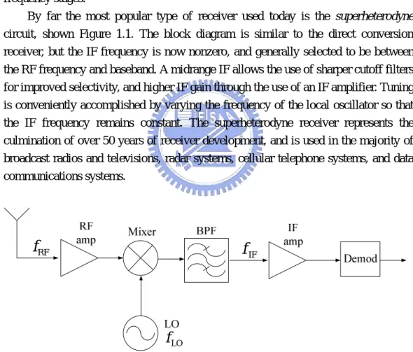
(21) l l l. Down-conversion from the received RF frequency to an IF frequency for processing. Detection of the received analog or digital information. Isolation from the transmitter to avoid saturation of receiver.. Because the typical signal power level from the receive antenna may be as low as -100 to -120 dBm, the receiver may be required to provide gain as high as 100 to 120 dB. This much gain should be spread over the RF, IF, and baseband stages to avoid instabilities and possible oscillation; it is generally good practice to avoid more than about 50-60dB of gain at any one frequency band. The fact that amplifier cost generally increases with frequency is a further reason to spread gain over different frequency stages. By far the most popular type of receiver used today is the superheterodyne circuit, shown Figure 1.1. The block diagram is similar to the direct conversion receiver, but the IF frequency is now nonzero, and generally selected to be between the RF frequency and baseband. A midrange IF allows the use of sharper cutoff filters for improved selectivity, and higher IF gain through the use of an IF amplifier. Tuning is conveniently accomplished by varying the frequency of the local oscillator so that the IF frequency remains constant. The superheterodyne receiver represents the culmination of over 50 years of receiver development, and is used in the majority of broadcast radios and televisions, radar systems, cellular telephone systems, and data communications systems.. f RF. f IF. f LO Figure 1.1. Block diagram of a single-conversion superheterodyne receiver. At microwave and millimeter wave frequencies it is often necessary to use two stages of down conversion to avoid problems due to LO stability. The dual-conversion superheterodyne receiver of Figure 1.2 employs two local oscillators and mixers to achieve down-conversion to baseband with two IF frequencies. 6.
(22) f RF. Figure 1.2. Block diagram of a double-conversion superheterodyne receiver. Figure 1.3 shows a graphical view of the input and output dynamic ranges of a typical receiver. The dynamic range of the input signal from the antenna is on the order of 100dB, while the output dynamic range of the receivers is typically about 60dB. The power gain through the receiver must therefore vary as a function of the input signal strength in order to fit the input signal range into the baseband processing range, for a wide range of input signal levels. A receiver gain on the order 60dB may be required for low level signals, while a gain of only 20-30dB may be required for high-level signals. This variable-gain function is accomplished with an automatic gain control (AGC) circuit. AGC is most often implemented at the IF stage, but some receivers may use AGC at the RF stage as well. Virtually all modern communications, broadcast radio, and television receivers use AGC to control signal levels.. Figure 1.3. Diagram illustrating the change in power levels between the input and output of a typical receiver.. 7.
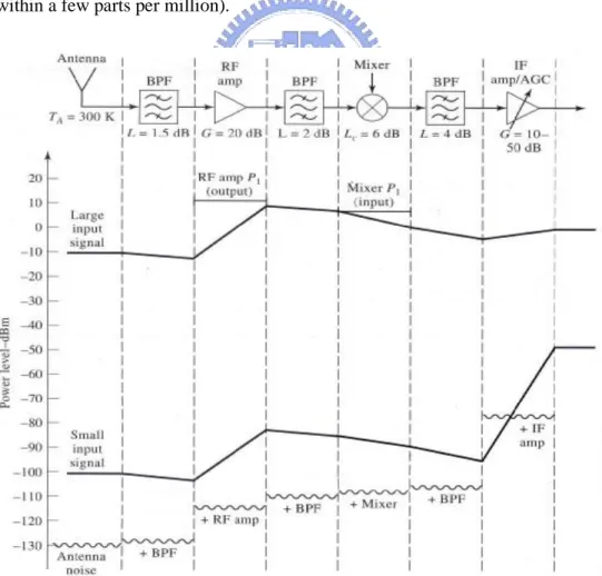
(23) The power levels of an amplifier that exceed the 1 dB compression point P1 will cause harmonic distortion, and power levels in excess of the third-order intercept point P3 will cause intermodulation distortion. Thus it is important to track power levels through the stages of the receiver to ensure that P1 and P3 are not exceeded. This can be conveniently done with a graph of the form shown in Figure 1.4. This diagram tracks the power level of small and large input signals, analog with the noise level (noise power or noise figure may be plotted), through the front-end stages of the receiver. The compression and third-order intercept points of the amplifiers and mixers can be plotted on the graph, making it easy to see if these limits are exceeded, and to determine the effect of changing component specifications or position in the receiver circuit. Oscillators are required in wireless receivers and transmitters to provide frequency conversion, and to provide sinusoidal sources for modulation. Typical transmitters and receivers may each use as many as 4-6 oscillators, at frequencies ranging from several kilohertz to many gigahertz. Often these sources must be tunable over a set frequency range, and must provide very accurate output frequencies (often to within a few parts per million).. Figure 1.4. Diagram of power and noise levels at consecutive stages of receiver 8.
(24) The simplest oscillator uses a transistor with an LC network to control the frequency of oscillation. Frequency can be tuned by adjusting the values of the LC network, perhaps electronically with a varactor diode. Such oscillators are simple and inexpensive, but suffer from the fact that the output frequency is very susceptible to variations in supply voltage, changing load impedances, and temperature variations. Better frequency control can be obtained by using a quartz crystal in place of the LC resonator. A crystal-controlled oscillator (XCO) can provide a very accurate output frequency, especially if the crystal is in a temperature controlled environment. Crystal oscillators, however, cannot easily be tuned in frequency. A solution to this problem is provided by the phase-locked loop (PLL), which uses a feedback control circuit and an accurate reference source (usually a crystal controlled oscillator) to provide an output that is tunable with high accuracy. Phase-locked loops and other circuits that provide accurate and tunable frequency outputs are called frequency synthesizers. Virtually all modern wireless systems rely on frequency synthesizer circuits for the key stages of frequency conversion. Important parameters that characterize frequency synthesizers are tuning range, frequency switching time, frequency resolution, cost, and power consumption. Another very important parameter is the noise associated with the output spectrum of the synthesizer, in particular the phase noise. Phase noise is a measure of the sharpness of the frequency domain spectrum of an oscillator, and is critical for many modern wireless systems.. 1.3 Organization of This Thesis It is the aim of this thesis to study the role of noise in the low noise amplifier (LNA) design and low phase noise VCO design. The noise figure plays important key for low noise amplifier circuit design. And the phase noise is another crucial property for oscillator design. In chapter2, the noise theory of the circuit is introduced. The content of the noise properties including the noise definition, noise spectrum, noise representation of the passive and active element will be described. The noise source property of the two port network is also mentioned. Especially, the characterization of noise figure on LNA and phase noise on VCO also included in this chapter. In chapter3, the design procedure of low noise amplifier is described first. Secondly, the structure of circuit topology of LNA with inductor feedback is used. Finally, the comparison of the simulation and measurement data is well matched for the performance with 4GHz low microwave band. Another circuit with 2.4GHz CMOS LNA was fabricated by the process of UMC 0.5um DPDM technology is also presented. We focus on the noise analysis of the circuit. 9.
(25) In chapter4, the basic design of microwave oscillator is described first. According to the concept of microwave oscillator design, the circuit structure with Complementary Cross-Coupled pair of voltage controlled oscillator is used. Secondly, the design methodology of VCO is mentioned. We proposed a new calculation method of the phase noise of VCO. The implementation of the VCO with the help of Chip Implementation Circuit (CIC) and Taiwan Semiconductor Manufacture Company (TSMC). The 0.35um 1P4M CMOS standard processes is employed. Finally, the proposed method of phase noise calculation is also compared to that of others. In chapter5, the short conclusion of our work and the view of the future work.. 10.
(26) Chapter 2 General Noise Theory 2.1 Introduction to Noise Concept Noise is a random process. This statement means the value of noise cannot be predicted ay any time even if the past values are known. Compare the output of a sinewave generator with that of a microphone picking up the sound of water flow in a river (Fig. 2.1). While the value of x1(t) at t = t1 can be predicted from the observed waveform, the value of x2(t) at t = t2 cannot. This is the principal difference between deterministic and random phenomena [4].. Figure 2.1. Output of a generator and the sound of a river. If the instantaneous value of noise in the time domain cannot be predicted, how can we incorporate noise in circuit analysis? This is accomplished by observing the noise for a long time and using the measured results to construct a “statistical model” 11.
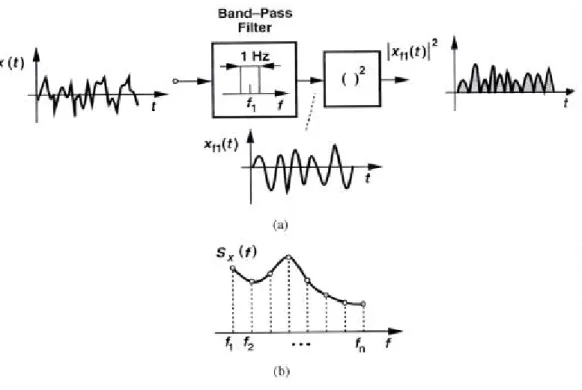
(27) for the noise. While the instantaneous amplitude of noise cannot be predicted, a statistical model provides knowledge about some other important properties of the noise that prove useful and adequate in circuit analysis. Which properties of noise can be predicted? In many cases, the average power of noise is predictable. The concept of average power proves essential in our analysis and must be defined carefully. Recall from basic circuit theory that the average power delivered by a periodic voltage v(t) to a load resistance RL is given by Pav =. 1 +T 2 v 2 (t ) dt T ∫−T 2 RL. (2.1). where T denotes the period. This quantity can be visualized as the average heat produced in RL by v(t). However, since the signals are not periodic, the measurement must be carried out over a long time: x 2 (t ) dt −T 2 R L. Pav = lim ∫ T →∞. +T 2. (2.2). where x(t) is a voltage quantity. Figure 2.2 illustrates the operation x2(t); each signal is squared, the area under the resulting wave form is calculated for a long time T, and the average power is obtained by normalizing the area to T.. Figure 2.2. Average noise power. To simplify calculations, we write the definition of Pav as 1 +T 2 2 x (t )dt T → ∞ T ∫−T 2. Pav = lim. (2.3). where Pav is expressed in V2 rather than W. The idea is that if we know Pav form (2.3), then the actual power delivered to a load RL can be readily calculated as Pav/RL. In analogy with deterministic signals, we can also define a root-mean-square (rms) voltage for noise as Pav where Pav is given by (2.3). The concept of average power becomes more versatile if defined with regard to frequency content of noise. The noise made by a group of men contains weaker 12.
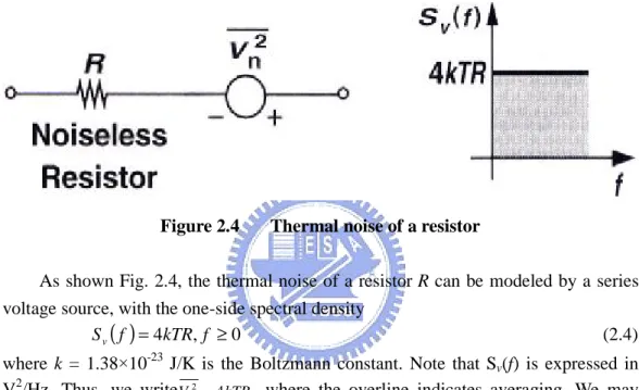
(28) high-frequency components than that made by a group of women, a difference observable from the “spectrum” of each type of noise. Also called the “power spectral density” (PSD), the spectrum shows how much power the signal carriers at each frequency. More specifically, the PSD, Sx(f), of a noise waveform x(t) is defined as the average power carried by x(t) in a one-hertz bandwidth around f. That is , as illustrated in Fig. 2.3(a), we apply x(t) to a bandpass filter with center frequency f1 and 1-Hz bandwidth, square the output, and calculate the average over a long time to obtain Sx(f1). Repeating the procedure with bandpass filters having different center frequencies, we arrive at the overall shape of Sx(f) [Fig. 2.3(b)]. While it is possible that the PSD of a random process is random itself, most of the noise sources of interest to us exhibit a predictable spectrum.. Figure 2.3. Calculation of noise spectrum. It is customary to eliminate RL from Sx(f). Thus, since each value of the plot in Fig. 2.3(b) is measured for a 1-Hz bandwidth, Sx(f) is expressed in V2/Hz rather than W/Hz. It is also common to take the square root of Sx(f), expressing the result in V Hz .. 2.2 Type of Noise Analog signals processed by integrated circuit are corrupted by two different type of noise: device electronic noise and environmental noise. We focus on device electronic noise here. There are three main fundamental noise mechanisms—thermal 13.
(29) noise, shot noise and flicker noise. 2.2.1 Thermal Noise Thermal noise is due to the thermal excitation of charge carriers in the conductor. It is also dependent on bias conditions. The random motion of electrons in a conductor introduces fluctuation is the voltage measured across the conductor even if the average current is zero. Thus, the spectrum of thermal noise is proportional to the absolute temperature.. Figure 2.4. Thermal noise of a resistor. As shown Fig. 2.4, the thermal noise of a resistor R can be modeled by a series voltage source, with the one-side spectral density S v ( f ) = 4kTR, f ≥ 0 (2.4) where k = 1.38×10⁻²³ J/K is the Boltzmann constant. Note that Sv(f) is expressed in V2/Hz. Thus, we writeVn2 = 4kTR , where the overline indicates averaging. We may even say the noise “voltage” is give by 4kTR even though this quantity is in fact the noise voltage squared. It should be mentioned here that thermal noise is also referred to as Johnson or Nyquist noise since it was first observed by J. B. Johnson [Johnson, 1928] and analyzed using the second law of thermodynamics by H. Nyquist [Nyquist, 1928]. 2.2.2 Shot Noise Shot noise was first studied by W. Schottky using vacuum-tube diodes [Schottky, 1918], but shot noise also occurs in pn junctions. This noise occurs because the dc bias current is not continuous and smooth but instead is a result of pulses of current caused by the individual flow of carriers. As such, shot noise is dependent on the dc bias current. It can also be modeled as a white noise source. Shot noise is also typically larger than thermal noise and is sometimes used to create white noise generators[5]. 14.
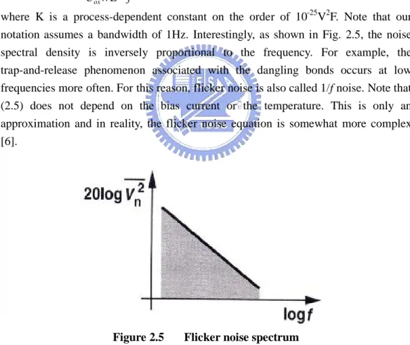
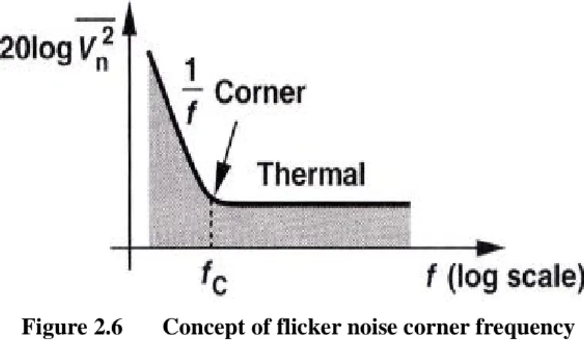
(30) 2.2.3 Flicker Noise Flicker noise is the least understood of the three noise phenomena. It is found in all active devices as well as in carbon resistors, but it occurs only when a dc current is flowing. Flicker noise usually arises due to traps in the semiconductor, where carriers that would normally constitute dc current flow are held for some time period and then released. Flicker noise is also commonly referred to as 1/f noise since it is well modeled as having a 1/fα spectral density, where α is between 0.8 and 1.3. Although both bipolar and MOSFET transistors have flicker noise, it is a significant noise source in MOS transistors, whereas it can often be ignored in bipolar transistor. The flicker noise of MOSFET is more easily modeled as a voltage source in series with the gate, and roughly given by K 1 (2.5) ⋅ Vn2 = C oxWL f where K is a process-dependent constant on the order of 10-25V2F. Note that our notation assumes a bandwidth of 1Hz. Interestingly, as shown in Fig. 2.5, the noise spectral density is inversely proportional to the frequency. For example, the trap-and-release phenomenon associated with the dangling bonds occurs at low frequencies more often. For this reason, flicker noise is also called 1/f noise. Note that (2.5) does not depend on the bias current or the temperature. This is only an approximation and in reality, the flicker noise equation is somewhat more complex [6].. Figure 2.5. Flicker noise spectrum. The inverse dependence of (2.5) on WL suggests that to decrease 1/f noise, the device area must be increased. It is therefore not surprising to see devices having areas of several thousand square microns in low-noise applications. It is also believed that PMOS devices exhibit less 1/f noise than NMOS transistors because the former 15.
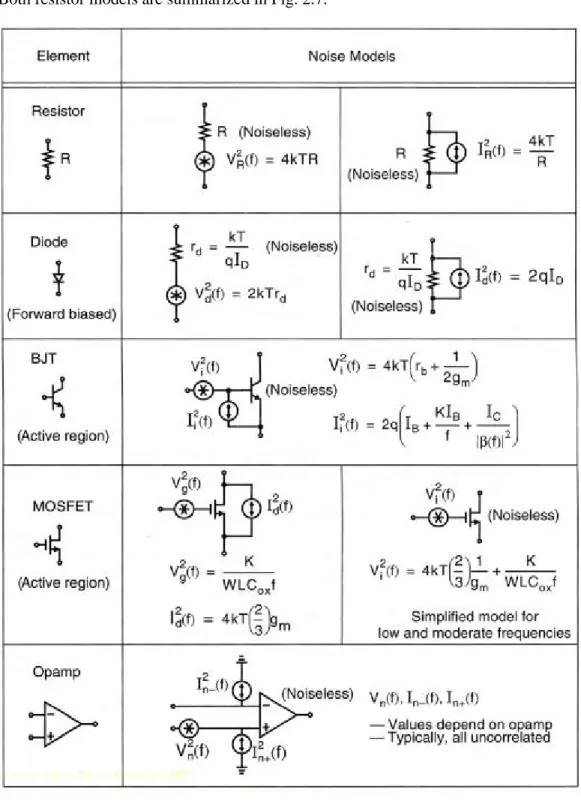
(31) carry the holes in a “buried channel”, i.e., at some distance from the oxide-silicon interface. Nonetheless, this difference between PMOS and NMOS transistors is not consistently observed [6].. Figure 2.6. Concept of flicker noise corner frequency. In order to quantify the significance of 1/f noise with respect to thermal noise for a given device, we plot both spectral densities on the same axes in Fig. 2.6. Called the 1/f noise “corner frequency”, the intersection point serves as a measure of what part of the band is mostly corrupted by flicker noise. In the above description, the 1/f noise corner, fC, of the output current is determined as K 3 (2.6) fC = gm C oxWL 8kT This result implies that fC generally depends on device dimensions and bias current. Nonetheless, since for a given L, the dependence is relatively weak, the 1/f noise corner is relatively constant, falling in the vicinity of 500KHz to 1MHz for submicron transistors [4]. 2.3 Noise Models for Circuit Elements [5] Resistors The major source of noise in resistors is thermal noise. As just discussed, it appears as white noise and can be modeled as a voltage source, VR(f), in series with a noiseless resistor. With such an approach, the spectral density function, V R2 ( f ) , is found to be given by V R2 ( f ) = 4kTR (2.7) -23 where k is Boltzmann’s constant (1.38×10 J/K), T is the temperature in Kelvins, and. R is the resistance size. An alternate model can be derived by finding the Norton equivalent circuit. Specifically, the series voltage noise source, VR(f), can be replaced with a parallel 16.
(32) current noise source, IR(f), given by VR2 ( f ) 4kT = R R2 Both resistor models are summarized in Fig. 2.7. I R2 ( f ) =. Figure 2.7. (2.8). Circuit elements and their noise modes. Note that capacitors and inductors do not generate noise.. 17.
(33) Diodes Shot noise is typically the dominant noise in diodes and can be modeled with a current source in parallel with the small-signal resistance of the diode, as Fig. 2.7 shows. The spectral density function of the current source is found to be given by I d2 ( f ) = 2qI D. (2.9). where q is one electronic charge (1.6×10⁻¹⁹ C) and ID is the dc bias current flowing through the diode. The small-signal resistance of the diode, rd, is given by the usual relationship, kT (2.10) rd = qI D Bipolar Transistors The noise in bipolar transistors is due to shot noise of both the collector and base currents, the flicker noise of the base current, and the thermal noise of the base resistance. A common practice is to combine all these noise sources into two equivalent noise sources at the base of the transistor, as shown in Fig. 2.7. Here, the equivalent input voltage noise, Vi(f), is given by 1 (2.11) Vi 2 ( f ) = 4kT rb + 2 gm where the rb term is due to the thermal noise of the base resistance and gm term is due to collector-current shot noise referred back to the input. The equivalent input current noise, Ii ( f ), equals KI IC I i2 ( f ) = 2q I B + B + 2 f β(f ) . . (2.12). where the 2qIB term is a result of base-current shot noise, the KIB/f term models 1/f noise (K is a constant dependent on device properties), and the IC term is the input-referred collector-current shot noise (it is often ignored). MOSFETS The dominant noise sources for active MOSFET transistors are flicker noise and thermal noise, as shown in Fig. 2.7. The flicker noise is modeled as a voltage source in series with the gate of value K (2.13) V g2 ( f ) = WLC ox f where the constant K is dependent on device characteristics and can very widely for 18.
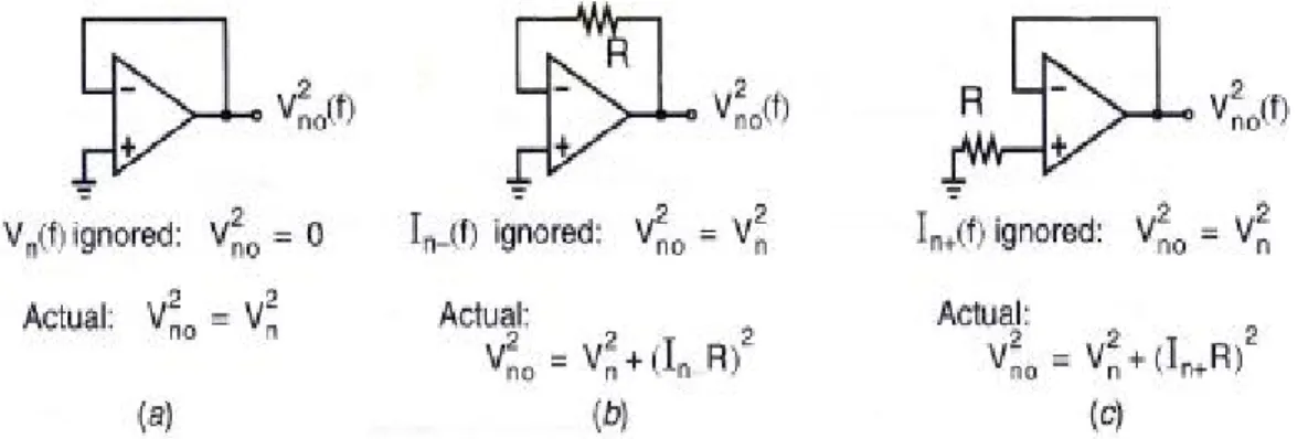
(34) different devices in the same process. The derivation of the thermal noise term is straightforward and is due to the resistive channel of a MOS transistor in the active region. If the transistor was in triode, the thermal noise current in the drain due to the channel resistance would simply be given by I d2 ( f ) = (4kT ) rds , where rds is the channel resistance. However, when the transistor is in the active region, the channel cannot be considered homogeneous, and thus, the total noise is found by integrating over small portions of the channel. Such an integration results in the noise current in the drain being given by I d2 ( f ) = 4kT γ g m. (2.14). the coefficient γ is derived to be equal to 2/3 for long-channel transistors and may need to be replaced by a larger value for submicron MOSFET [7]. The exact value of this number is under active research. Opamps Noise in poamps is modeled using three uncorrelated input-referred noise sources, as shown Fig. 2.7. With an opamp that has a MOSFET input stage, the current noise can often be ignored at low frequencies since their values are small. However, for bipolar input stages, all three noise sources are typically required, as shown in Fig. 2.8. In Fig. 2.8(a), if Vn(f) is not included in the model , a unity-gain buffer with no resistors indicates that the circuit output is noiseless. In fact, the voltage noise source, Vn(f), dominates. If In-(f) is not included in an opamp model, the circuit shown in Fig. 2.8(b) indicates that the output noise voltage equals Vn(f). Here, the current noise may dominate if the resistance, R, is larger. A similar conclusion can be drawn with In+(f), as shown in Fig. 2.8(c).. Figure 2.8. Opamp circuits showing the need for three noise source in an opamp noise model. Assume the resistance, R, is noiseless is simplified from Vn(f) to Vn, and so on. 19.
(35) 2.4 Noise Theory Apply to RF Circuit In this section, we focus on the noise theorem applying to RF circuit design. The first circuit is the low noise amplifier (LNA) with using MESFET for 4GHz band transmission. The noise figure plays important role for LNA. Therefore, the noise figure represented by two port network will be described. The second circuit is the oscillator at 2GHz signal generation with using MOSFET to fabricate the integrated circuit under voltage controlled. Deal with oscillator property, the phase noise shows the critical parameter for circuit design. In the following, noise figure and phase noise will be introduced separately. 2.4.1 Definition of Noise Figure by Two-Port Network. Figure 2.9. (a) Noisy two-port network; (b) noiseless two-port representation.. It is well know that the maximum noise power that a noisy resistor can deliver to a network within the bandwidth B is PN =. Vn2,rms. (2.15) = kTB 4R Next, we consider the noise characterization of a two-port network. A two-port network is shown in Fig. 2.9, where the available input noise power from the resistor Rs at temperature Ts is PNi = kTsB. This input noise power gets amplified by the available gain of the two-port network (GA) and appears at the output. In addition, the noisy two-port network contributes a certain amount of noise power to the output, shown as Pn in Fig. 2.9a. The total available noise power at the output is PN o = G A PN i + PN = G A kTs B + PN. (2.15). Associated with Pn, we can define an effective input noise temperature Te such that Te =. Pn kBG A. (2.16). 20.
(36) The noise figure F of a two-port network at a specific signal frequency is defined as [9] F=. PN o PNi G A. =. total available noise power at the output amplify the available noise power at the input. By some manipulation, the noise figure is T F = 1+ e Ts. (2.17). (2.18). 2.4.2 Oscillator Phase Noise For a nominally periodic sinusoidal signal, we can write x(t ) = A cos[ω c t + φ n (t )] , where φ n (t ) is a small random excess phase representing variations in the period. The function φ n (t ) is “called phase noise”. Note that for φ n (t ) << 1 rad, we have x(t ) ≈ A cos ω c t − Aφ n (t )sin ω c t ; that is, the spectrum of φ n (t ) is translated to ± ω c .. In RF applications, phase noise is usually characterized in the frequency domain. For an ideal sinusoidal oscillator operating at ω c , the spectrum assumes the shape of an impulse, whereas for an actual oscillator, the spectrum exhibits “skirts” around the carrier frequency in Fig. 2.10. To quantify phase noise, we consider a unit bandwidth at an offset ∆ω with respect to ω c , calculate the noise power in this bandwidth, and divide the result by the carrier (average) power [10].. Figure 2.10. Output spectrum of ideal and actual oscillators.. Phase noise is defined as the ratio of power in one phase modulation sideband to the total signal power per unit bandwidth (one Hertz) at a given offset; fm, from the signal frequency, and is denoted as L( f m ) . It is usually expressed in decibels relative to the carrier power per Hertz of bandwidth (dBc/Hz). A typical oscillator phase noise 21.
(37) specification for an FM cellular radio, for example, may be -110dBc/Hz at 25KHz from the carrier. In general, the output voltage of an oscillator or synthesizer can be written as [1]: vo (t ) = V0 [1 + A(t )]cos[ω 0 t + θ (t )] (2.19) where A(t) represents the amplitude fluctuations of the output, and θ(t) represents the phase variation of the output waveform. Of these, amplitude variations can usually be well controlled, and generally have less impact on system performance. Small changes in the oscillator frequency can be represented as a frequency modulation of the carrier by letting ∆f (2.20) θ (t ) = sin ω m t = θ p sin ω m t fm where f m = ω m 2π is the modulating frequency. The peak phase deviation is θ p = ∆f f m (also called the modulation index). Substituting (2.20) into (2.19) and expanding gives. [. ]. vo (t ) = V0 cos ω 0 t cos (θ p sin ω m t ) − sin ω 0 t sin (θ p sin ω m t ). (2.21). where we set A(t) = 0 to ignore amplitude fluctuations. Assuming the phase deviations are small, so that θ p <<1, the small argument expressions that sin x ≅ x and cos x ≅ 1 can be used to simplify (2.21) to. [. vo (t ) = V0 cos ω 0 t − θ p sin ω m t sin ω 0 t. ]. θp (2.22) = V0 cos ω 0 t − [cos(ω 0 + ω m )t − cos(ω 0 − ω m )t ] 2 This expression shows that small phase or frequency deviations in the output of an oscillator result in modulation sidebands at ω 0 ± ω m , located on either side of carrier signal at ω 0 . When these deviations are due to random changes in temperature or device noise, the output spectrum of the oscillator will take the form shown in Figure 2.10. According to the definition of phase noise as the ratio of noise power in a singale sideband to the carrier power, the waveform of (2.22) has a corresponding phase noise of 1 V0θ p Pn 2 2 L( f ) = = 1 2 Pc V0 2 where θ rms = θ p. 2. 2 2 = θ p = θ rms 4 2. (2.23). 2 is the rms value of the phase deviation. The two-sided power. spectral density associated with phase noise includes power in both sidebands:. 22.
(38) Sθ ( f m ) = 2 L( f m ) =. θ p2 2. 2 = θ rms. (2.24). 2.4.3 Leeson’s Model for Phase Noise. Figure 2.11. feedback amplifier model for characterizing oscillator phase noise.. In this section we present Leeson’s model for characterizing the power spectral density of oscillator phase noise [9], [11]. We will model the oscillator as an amplifier with a feedback path, as shown in Figure 2.11. If the voltage gain of the amplifier is included in the feedback transfer function H (ω ) , then the voltage transfer function for the oscillator circuit is V0 (ω ) =. Vi (ω ) 1 − H (ω ). (2.25). If we consider oscillators that use a high-Q resonant circuit in the feedback loop, the H (ω ) can be represented as the voltage transfer function of a parallel RLC resonator [4]: H (ω ) =. 1. =. 1 1 + 2 jQ ∆ω ω 0. (2.26) ω ω0 − 1 + jQ ω0 ω where ω 0 is the resonant frequency of the oscillator, and ∆ω = ω − ω 0 is the offset relative to the resonant frequency. We know that the input and output power spectral densities are related by the square of the magnitude of the voltage transfer function, so we can use (2.25) to write 2. 1 + 4 Q 2 ∆ω 2 ω 02 1 S φ (ω ) = Sθ (ω ) = Sθ (ω ) 1 − H (ω ) 4Q 2 ∆ω 2 ω 02. 23.
(39) ω 02 = 1 + 2 2 4Q ∆ω. ω2 S θ (ω ) = 1 + h 2 ∆ω. Sθ (ω ) . (2.27). where Sθ (ω ) is the input PSD, and Sφ (ω ) is the output PSD. In (2.27) we have also defined ω h = ω 0 2Q as the half-power (3dB) bandwidth of the resonator.. Figure 2.12. Noise power versus frequency for an amplifier with an applied input signal.. The noise spectrum of a typical transistor amplifier with an applied sinusoidal signal at f0 is shown in Figure 2.12. Besides kTB thermal noise, transistors generate additional noise that varies as 1/f at frequencies below the frequency fα. This 1/f, or flicker noise is likely caused by random fluctuations of the carrier density in the active device. Due to the nonlinearity of the transistor, the 1/f noise will modulate the applied signal at f0, and appear as 1/f noise sidebands around f0. Since the 1/f noise component dominates the phase noise power at frequencies close to the carrier, it is important to include it in our model. Thus we consider an input power spectral density as shown in Figure 2.13, where K / ∆f represents the 1/f noise component around the carrier, and kT0F/P0 represents thermal noise. Thus the power spectral density applied to the input of the oscillator can be written as kT0 F Kωα (2.28) 1 + P0 ∆ω where K is a constant accounting for the strength of the 1/f noise, and ωα = 2πf α is Sθ (ω ) =. the corner frequency of the 1/f noise. The corner frequency depends primarily on the type of transistor used in the oscillator.. 24.
(40) Figure 2.13. Idealized power spectral density of amplifier noise, including 1/f and thermal components.. Using (2.28) in (2.27) gives the power spectral density of the output phase noise as S φ (ω ) =. =. kT0 F Kω 02ωα ω 02 Kω α + + + 1 2 3 2 2 ∆ω P0 4Q ∆ω 4Q ∆ω kT0 F Kωα ω h2 ω h2 K∆ ω α + + + 1 3 2 P0 ∆ω ∆ω ∆ω . This result is sketched of the middle two terms of close to the carrier f0, the resonator has a relatively. (2.29). in Figure 2.14. There are two cases, depending on which (2.29) is more significant. In either case, for frequencies noise power decreases as 1/f3, or -18dB/octave. If the low Q, so that its 3dB bandwidth f h > f α , then for. frequencies between fα and fh the noise power drops as 1/f 2, or -12dB/octave. If the resonator has a relatively high Q, so that f h < f α , then for frequencies between fh and fα the noise power drops as 1/f, or -6dB/octave.. Figure 2.14. Power spectral density of phase noise at the output of an oscillator. (a) response for f h > f α (low Q). (b) response for f h < f α (high Q). 25.
(41) Chapter 3 Microwave Low Noise Amplifier with Source Inductance Feedback 3.1 Introduction The first stage of a receiver is typically a low-noise amplifier (LNA), whose main function is to provide enough gain to overcome the noise of subsequent stages (such as a mixer). Aside from provide this gain while adding as little noise as possible, an LNA should accommodate large signals without distortion, and frequency must also present a specific impedance, such as 50Ω, to the input source[9].Recently, Source inductive feedback (SIF) has found its applications in the low noise amplifiers by MMIC and CMOS IC technologies[12-15]. The noise properties of amplifiers are described typically by minimum noise figure F min , equivalent noise resistance R n and optimal reflection coefficient Γopt . A low noise amplifier is normally designed to have the source reflection coefficient Γs equal to Γopt to obtain the lowest noise figure F min , at the expanse of the return loss. The technique of SIF can introduce equivalently a resistor to achieve input impedance and noise matching simultaneously, and even slightly reduce both F min and R n [16-20]. As the frequency is raised, this technique may fail. The package parasitic is conjectured to be the crucial role. But until now, a study of the relationship between FET parameter and SIF inductance has not been detailed. The information of frequency limitations of SIF in package device are also not available. It is interesting to study the universality of the technique, especially in the discrete circuit design for practical applications. Due to the circuit complexity, the studies are explored by numerical computation. We study the noise problem with a noisy two-port network [21,22,23,24]. In section 3.2, the generic behaviors of packaged MESFET with SIF at various frequencies region are examined from the two-port scattering and noise parameters. In section 3.3, the equivalent small signal model with noise sources are extracted. The mechanisms of degradation in F min are elucidated by inspecting each element of the model. Finally, the frequency limitation of SIF technique in the package device is indicated.. 3.2 Calculations of Noise Parameters 3.2.1 Low-Noise Amplifier Design 26.
(42) Besides stability and gain, another important design consideration for a microwave low noise amplifier is its noise figure. In receiver applications especially, it is often required to have a preamplifier with as low a noise figure as possible , the first stage of a receiver front end has the dominate effect on the noise performance of the overall system. Generally it is not possible to obtain both minimum noise figure and maximum gain for an amplifier, so some sort of compromise must be made. This can be down by using constant gain circles and circles of constant noise figure to select a usable trade-off between noise figure and gain. Here we will derive the equations for constant noise figure circles, and show how they are used in transistor amplifier design. As derived in references [1,8,9], the noise figure of a two-port amplifier can be expressed as. F = F min +. RN Y S − Y opt GS. 2. (3.1). where the following definitions apply: YS = GS + j BS = source admittance presented to transistor. Yopt = optimum source admittance that results in minimum noise figure. Fmin = minimum noise figure of transistor, attained when YS = Yopt. RN = equivalent noise resistance of transistor. GS = real part of source admittance. Instead of the admittance YS and Yopt, we can use the reflection coefficients Γs and Γopt , where. Y. S. =. Y opt =. 1 1 − Γ Z 0 1 + Γ. S. (3.2a). S. 1 1 − Γ opt Z 0 1 + Γ opt. (3.2b). Γs is the source reflection coefficient . The quantities Fmin, Γopt , and RN are characteristics of. the particular transistor being used, and are called the noise. parameters of the device;. they may be given by the manufacturer, or measured.. Using (3.2), the quantity YS − Yopt. YS − Yopt. 2. =. ΓS − Γopt. 4 2. 2. can be expressed in terms of Γs and Γopt :. 2. Z0 1+ Γ 2 1+ Γ S opt. (3.3). 2. 27.
(43) Also, * 1 1 − ΓS 1 − ΓS 1 1 − ΓS + )= G S = Re{YS } = ( * 2 Z 0 1 + ΓS 1 + ΓS Z0 1+ Γ S. 2 2. (3.4). Using these results in (3.1) gives the noise figure as 2. F = Fmin. ΓS − Γopt 4RN + Z 0 (1 − Γ 2 ) 1 + Γ S opt. (3.5). 2. For a fixed noise figure, F, we can show that this result defines a circle in the Γs plane. First define the noise figure parameter, N, as Γ S − Γ opt. N =. 1 − ΓS. 2. 2. F − F min 1 + Γ opt 4RN / Z 0. =. 2. (3.6). which is constant, for a given noise figure and set of noise parameters. Then rewrite (3.6) as (ΓS − Γopt )(ΓS − Γopt ) = N (1 − ΓS ), *. 2. *. ΓS ΓS − (ΓS Γopt + ΓS Γopt ) + Γopt Γopt = N − N ΓS , *. *. *. (ΓS Γopt + ΓS Γopt ) *. ΓS ΓS − *. Now add Γopt. ΓS −. Γopt N +1. *. N +1 2. 2. *. =. 2. N − Γopt. ,. N +1. ( N + 1) 2 to both sides to complete the square to obtain 2. =. N ( N + 1 − Γopt ) ( N + 1). (3.7). ,. This result defines circles of constant noise figure with centers at CF =. Γopt N +1. ,. (3.8). and radii of 2. RF =. N ( N + 1 − Γopt ). (3.9). N +1. 3.2.2 Noise Two-port Network Theory of Cascode Connection First, the generic behaviors of packaged MESFET with SIF shown in Fig.3.1 are examined through the noise and scattering parameters. In general, the noise parameters are in terms of F min , R n and Γopt in the data sheet of Table 3.1. 28. The.
(44) Fig.3.1 Block diagram of the single stage microwave amplifier with SIF. Table 3.1. NEC NE42484A under Vds = 2V and Ids = 10mA. 29.
(45) noise figure F is described again as [17]. 2 R F = Fmin + n Ys − Yopt Gs. (3.10). where Ys = G s + jBs represents the source admittance, and Yopt is the optimum admittance. The admittance Yopt is equal to:. Yopt = Gopt + jBopt =. 1 − Γopt 1 + Γopt. Y0. (3.11). For convenience, another form of noise figure is given by: F = 1+. rn + g n Z s + Z c. 2. (3.12). Rs. where rn is the equivalent normalized noise resistance, g n is the equivalent normalized noise conductance [25], and Z c is the correlation impedance. Their interrelations are given as:. rn =. ( 4 Rn Gopt − Fmin + 1 )( Fmin − 1 ) 4 Rn Yopt. g n = Rn Yopt Zc =. (3.13). 2. 2. (3.14). Fmin − 1 − 2RnGopt + j 2Rn Bopt 2Rn Yopt. 2. = Rc + jX c. (3.15). Inversely, we also get another form of noise figure as following: Fmin = 1 + 2 g n ( Rc + Ropt ). (3.16). After SIF is added , new parameters rnt 、 g nt and Z ct with subscript t denoted as total are represented as follows [22]: r nt = rn. g nt = D n Z ct =. (3.17) 2. gn. (3.18). Z c + En = Rct + jX ct Dn. (3.19). where. 30.
(46) En = − Z11a +. Dn =. ( Z11a + Z11b ) Z 21a ( Z 21a + Z 21b ). (3.20). Z 21a Z 21a + Z 21b. (3.21). and Z ija and Z ijb , I, j=1,2 represent the element of the impedance matrix of the transistor in network Na and the external inductor in network Nb, respectively. The inductance involved by Nb network is Z11b = jωL and Z21b = jωL. Accordingly, from (3.13) to (3.16) the new noise figure, noise resistance, and optimal admittance with SIF become:. Fmin t = 1 + 2 g nt Rct + g nt rnt + (g n Rc )2 Rnt = rnt + g nt Z ct rnt Y optt =. g nt. rnt. 2. (3.22) (3.23). + R ct2 + jX ct. g nt. + Z ct. (3.24). 2. and then 1− Γoptt = 1+. Yoptt Y0 Yoptt. (3.25). Y0. Hereafter, the subscript t is dropped for convenience. The scattering parameters are also changed as the inductor is included into the active device . They are obtained via a numerical manipulation of two to three port transformations [18,21]. To obtain the noise and gain matching, the portraits of new Γin* and Γopt in the Smith chart as a function of feedback inductance are calculated. Here, Γin* is further replaced by S11* under the assumption of small S12 . In fact, the behavior of Γin* is by no means more complicated than S11 . The S11 acts as a precursor of Γin . This approach gives us a quick examination.. 31.
數據
+7

相關文件
Chou, “The Application on Investigation of Rice Field Using the High Frequency and High Resolution Satellite Images (1/3)”, Agriculture and Food Agency, 2005. Lei, “The Application
Then, we tested the influence of θ for the rate of convergence of Algorithm 4.1, by using this algorithm with α = 15 and four different θ to solve a test ex- ample generated as
Numerical results are reported for some convex second-order cone programs (SOCPs) by solving the unconstrained minimization reformulation of the KKT optimality conditions,
Particularly, combining the numerical results of the two papers, we may obtain such a conclusion that the merit function method based on ϕ p has a better a global convergence and
Then, it is easy to see that there are 9 problems for which the iterative numbers of the algorithm using ψ α,θ,p in the case of θ = 1 and p = 3 are less than the one of the
By exploiting the Cartesian P -properties for a nonlinear transformation, we show that the class of regularized merit functions provides a global error bound for the solution of
In this paper we establish, by using the obtained second-order calculations and the recent results of [23], complete characterizations of full and tilt stability for locally
Jesus falls the second time Scripture readings..
![TraditionalMLCalgorithmsmainlytacklethebatchMLCproblem,wheretheinputdataarepresentedinabatch[24,28].Nevertheless,inmanyMLCapplicationssuchase-mailcategorization[22],multi-labelexamplesarriveasastream.Onlineanalysisistherefore dimensionreducermotivatedbyma](data:image/gif;base64,R0lGODlhAQABAIAAAP///wAAACH5BAEAAAAALAAAAAABAAEAAAICRAEAOw==)