國
立
交
通
大
學
電機學院光電顯示科技產業研發碩士班
碩
碩
碩
碩
士
士
士
士
論
論
論
論
文
文
文
文
溶膠凝膠氧化鋅薄膜電晶體氧化處理之研究
Study of Sol-Gel ZnO thin film transistor with oxidation
treatment
研 究 生:黃千睿 Chien-Jui Huang
指導教授:劉柏村 教授 Dr. Po-Tsun Liu
中
中
中
中
華
華
華
華
民
民
民
民
國
國
國
國
九
九
九
九
十
十
十
十
六
六
六
六
年
年
年
年
一
一
一
一
月
月
月
月
溶膠凝膠氧化鋅薄膜電晶體氧化處理之研究
Study of Sol-Gel ZnO thin film transistor with oxidation
treatment
研 究 生:黃千睿 Student:Chien-Jui Huang
指導教授:劉柏村 Advisor:Po-Tsun Liu
國 立 交 通 大 學
電機學院光電顯示科技產業研發碩士班
碩 士 論 文
A ThesisSubmitted to College of Electrical and Computer Engineering National Chiao Tung University
in partial Fulfillment of the Requirements for the Degree of
Master in
Industrial Technology R & D Master Program on Photonics and Display Technologies
January 2007
溶膠凝膠氧化鋅薄膜電
溶膠凝膠氧化鋅薄膜電
溶膠凝膠氧化鋅薄膜電
溶膠凝膠氧化鋅薄膜電晶體氧化處理之研究
晶體氧化處理之研究
晶體氧化處理之研究
晶體氧化處理之研究
學生:黃千睿 指導教授:劉柏村
國立交通大學光電顯示產業研發碩士班
摘
要
氧化鋅(ZnO) 是一個透明的半導體,能隙為 3.7eV 介於可見光不吸收的區域。此透 明氧化鋅薄膜電晶體有對光不敏感,高開口率,高載子移動率的特性。 本論文研製之氧化鋅薄膜電晶體是使用溶膠凝膠(sol-gel)的方式來製造,此方式是 利用一種旋塗沉積的技術(spin-on-deposition)來形成氧化鋅薄膜,並且可以在常壓常 溫下形成氧化鋅薄膜,相較於傳統的真空濺鍍系統(DC Sputter, RF Sputter),旋塗沉 積的技術可以節省很多製程上面的成本以及時間。 氧化鋅溶膠凝膠是以醋酸鋅為主要原料,水當作水解劑,先合成溶膠;再將此溶膠 加入異丙醇當中攪拌並且升溫到 60℃,溶膠中粒子鍵結成網狀的分子態稱為凝膠。 氧化鋅薄膜在旋塗沉積之後,我們使用退火及雙氧水氧化方式來改善氧化鋅薄膜電 晶體的特性,並且利用改變溫度、氧氣壓力及摻雜的方式來找出最好條件。我們使用不 同的烘烤(Baking)方式來去除水氣和改善薄膜的均勻性,並且找出去除有機鍵的溫度。 此外,我們使用摻雜鋯元素方式當作雜質,因而使得氧化鋅容易擁有半導體特性。 我們使用 SEM、N&K、FTIR、EDS、AFM、TDS 來分析溶膠凝膠氧化鋅薄膜的材料特性, 並使用 I-V 量測裝置(4156)來探討氧化鋅薄膜電晶體的電性趨勢。
Study of Sol
Study of Sol
Study of Sol
Study of Sol-
--
-Gel ZnO thin film transistor
Gel ZnO thin film transistor
Gel ZnO thin film transistor
Gel ZnO thin film transistor
with oxidation
with oxidation
with oxidation
with oxidation
treatment
treatment
treatment
treatment
student:
Chien-Jui HuangAdvisors:Dr.
Po-Tsun LiuDepartment﹙Institute﹚of Industrial Technology R & D Master Program on
Photonics and Display Technologies
National Chiao Tung University
ABSTRACT
Zinc oxide(ZnO) is a transparent semiconductor , it’s band gap is 3.3eV in the visible region of the spectra and therefore, also less light sensitive .This transparent zinc-oxide thin film transistor have character of less light sensitive、higher opening of AMLCD pixel、higher mobility.
ZnO TFT was fabricated by sol-gel .Sol-Gel is a spin-on-deposition technology. We can use this way to form ZnO thin film in the room temperature(RT) and room pressure (RP) environment. The process of spin-costing deposition provides a more efficient way for depositing device components and low cost than vacuum techniques.
In addition, we dope Zr element in ZnO solutions to form ZrZnO thin film in order to decrease the grain size of ZnO. We can use this way to get a ZnO show a semiconductor characteristic.
When we finish the process of spin-costing deposition , we improve the ZNO-TFT character by different annealing temperature 、pressure and other oxidiative method. We also improve the zno film uniform by different baking method, then we can get an optimal condition.
誌
謝
首先誠摯的感謝指導教授劉柏村教授,老師悉心的教導使我得以一窺
氧化鋅薄膜電晶體領域的深奧,不時的討論並指點我正確的方向,使我在
這碩士生涯中獲益匪淺。另外,還要感謝中山物理系張鼎張教授在學術研
究上給我的指導,使我的研究可以更為順利。
兩年裡的日子,實驗室裡共同的生活點滴,學術上的討論、言不及義
的閒扯、熬夜約機台的等待、趕作業的革命情感你們的陪伴讓兩年的研究
生活變得絢麗多彩。
在此,特別感謝黃震鑠學長不厭其煩的指出我研究中的缺失並提供我
意見,且總能在我無助時為我解答,也感謝昇翰、子怡同學的幫忙,恭喜
我們順利走過這兩年。還要感謝秀娟、柏宇、宛芳在NDL裡蹲苦窯的日子裡
有你們的參與協助。實驗室的建名、誼明、崇維、啟銘、唐豪、逸侑、亞
諭、又菁學弟們當然也不能忘記,有你們在讓這兩年更加有趣。
最後,謹以此文獻給我摯愛的雙親、祖父祖母以及我的妹妹,由於你
們的默默支持更是我前進的動力,有你們的體諒、包容,這兩年的生活擁
有很不一樣的光景。
Contents
ABSTRACT(CHINESE) ...I
ABSTRACT(ENGLISH) ...II
ACKNOWLEDGEMENTS ...III
CONTENTS ... IV
TABLE CAPTIONS ... VI
FIGURE CAPTIONS ... VII
CHAPTER 1. INTRODUCTION
1-1 General Background ...……..1
1-2 Motivation...2
CHAPTER 2. EXPERIMENTAL PROCEDURES
2-1 TFT Fabrication ...4
2-2 Experimental Procedures ...5
2-2-1 spin-coating deposition...6
2-2-2 Changing Baking Temperature ...7
2-2-3 Patterning ...7
2-2-4 Changing Annealing Temperature...8
2-2-5 Changing Annealing Pressure ...9
2-2-6 Hydrogen peroxide oxidation ...10
CHAPTER 3 RESULTS AND DISCUSSIONS
3-1 ZnO Film Analisys
...
12
3-1-1 The FTIR Measurement of ZnO and Films ...12
3-1-2 The FTIR Measurement of Zr
0.03Zn
9.97O and Films ...12
3-1-4 The AFM Measurement of ZnO Films ...14
3-1-5 The TDS Measurement of ZnO Films ...15
3-2 The Electrical Characteristics of ZnO based TFTs ...16
3-2-1 Baking with various temperature...16
3-2-2 Annealing with various temperature...17
3-2-3 Annealing with various oxygen pressure...18
3-2-4 Hydrogen peroxide oxidation ...19
3-2-5 Zr
0.03Zn
9.97O based TFTs...20
CHAPTER 4 CONCLUSION
REFERENCES
Table captions
Chapter1
Table 1 shows experimental flow path in my experiment.
Chapter2
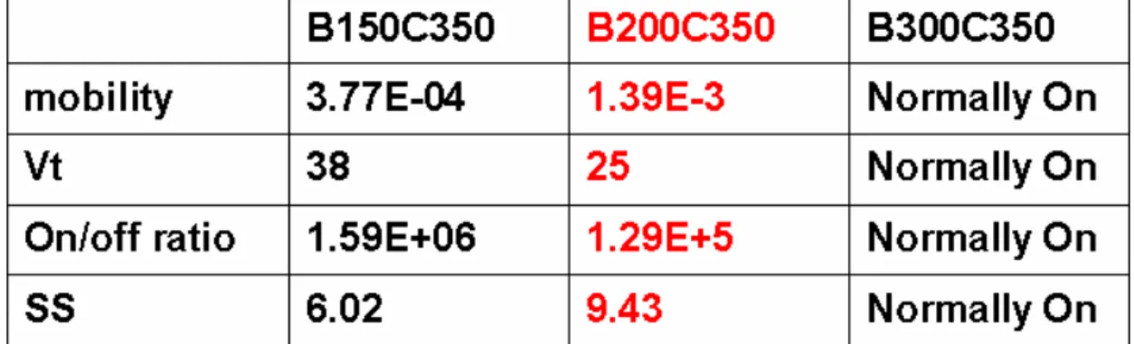
Table 2 shows the material characteristic of the ZnO thin films with different baking conditions.
Table 3 shows electronic properties of ZnO-base TFTs with different baking conditions.
Table 4 shows electronic properties of ZnO-base TFTs with different curing conditions.
Figure captions
Chapter1
Figure1-1 shows the hexagonal wurtize structure of Zinc Oxide
Chapter2
Figure2-1 shows a device structure of Zn1−xZrxO-TFTs Figure2-2 shows a device structure of ZnO-TFTs
Chapter3
Figure3-1 shows the corresponding peaks of FTIR for ZnO
Figure3-2 illustrates the FTIR measurement result of varied baking temperature ZnO film on a single crystalline Silicon substrate
Figure3-3 illustrates the FTIR measurement result of varied Curing temperature ZnO film on a single crystalline Silicon substrate
Figure3-4 illustrates the FTIR measurement result of varied environment ZnO film on a single crystalline Silicon substrate.
Figure3-5 illustrates the FTIR measurement result of varied Curing temperature ZrZnO film on a single crystalline Silicon substrate
Figure3-6 shows the corresponding peaks of FTIR for ZrO
Figure3-7 illustrates the SEM measurement result of the ZnO thin films anneal under 350°C oxygen environment.
Figure3-8 illustrates the SEM measurement result of the ZnO thin films anneal under 500°C oxygen environment.
Figure3-9 illustrates the SEM measurement result of the ZnO thin films anneal under 350°C vacuum environment.
Figure3-10 illustrates the AFM measurement result of the ZnO thin films baking at 150°C under oxygen environment.
Figure3-11 illustrates the AFM measurement result of the ZnO thin films baking at 200°C under oxygen environment.
Figure3-12 illustrates the AFM measurement result of the ZnO thin films baking at 30°C under oxygen environment.
Figure3-13 lustrates the TDS measurement result of the Sputter ZnO thin films. Figure3-14 illustrates the TDS measurement result of the Sputter ZnO thin films of capping Nitride.
Figure3-15 shows the ID-VG of comparison between baking temperature150~300°C
by hotplate
Figure3-16 shows the ID-VD of our devices with the conditions of baking at 200°C for 10
min
Figure3-17 shows the ID-VG of ZnO TFT after stress
Figure3-18 show the ID-VG of our devices with the condition of annealed under 0.3 torr
torr oxygen ambient with temperature 350°C for 1 hr
Figure 3-20 shows the ID-VG of our devices with the condition of annealed at 350°C under oxygen ambient with pressure vacuum, 0.3 , 0.6 torr for 1 hr.
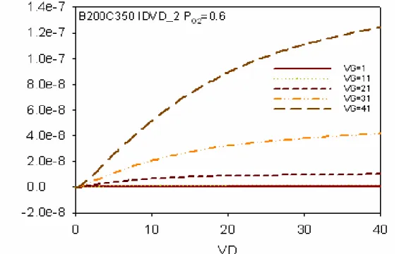
Figure 3-21 shows the ID-VD of our devices with the condition of annealed at 350°C under oxygen ambient with pressure 0.6 torr for 1 hr
Figure 3-22 shows the threshold voltage and mobility of the different curing pressure Figure 3-23(a) show the ID-VG of our devices with the condition of annealed under
Room Pressure furnace.
Figure 3-23(b) show the ID-VD of our devices with the condition of annealed under
Room Pressure furnace
Figure 3-24 shows the different conditions of treat with H2O2
Figure3-25 shows the ID-VG of our devices with different condition of treat with H2O2.
Figure3-26 shows the ID-VG of our devices with the condition of annealed under 0.3 torr oxygen ambient with different temperature 350 425 500°C
Figure 3-27 shows the threshold voltage and mobility of the different curing temperature for ZrZnO TFTs
Figure 3-28 shows the ID-VG of ZrZnO devices with the condition of annealed at 350°C under oxygen ambient with pressure vacuum, 0.3, 0.6 torr
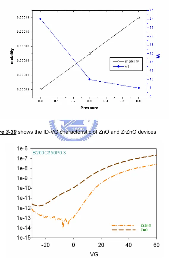
Figure 3-29 shows the threshold voltage and mobility of the different curing pressure for ZrZnO
Chapter 1 Introduction
1-1 General Background
Transparent electronics are nowadays an emerging technology for the next generation of optoelectronic devices. The fundamental device that enables the realization of transparent circuits is a transparent transistor. The only possibility to perform transparent transistors is by using oxide semiconductors. Oxide semiconductors are very interesting materials becausethey combine simultaneously high/low conductivity with high visual transparency and have been widely used in a variety of applications (e.g. antistatic coatings, touch display panels, solar cells, flat panel displays, heaters, defrosters, optical coatings, among others). Transparent oxide semiconductor-based transistors have recently been proposed, using as active
channel intrinsic zinc oxide (ZnO). The main advantage of using ZnO deals with the fact that it is possible to growth at near room temperature high quality polycrystalline zinc oxide, which is a particular advantage for electronic drivers, where the response speed is of major importance. Besides that, since ZnO is a wide band gap material (3.2 eV), it is transparent in the visible regionof the spectra and therefore, also less light sensitive.
channel is conductive without applying gate bias. This phenomenon may be attributed to the as-deposited ZnO thin films containing high carrier densities, thus increasing the conductivity in the channel. Hence, one of the most important works in ZnO-based TFTs research efforts is to reduce the carrier concentration in ZnO thin films. Since it has been demonstrated that the ZnO films exhibited a lower carrier concentration with a higher annealing temperature. In this study, we investigated the properties of sol-gel derived Zr-doped ZnO films at a low annealing temperature of 350°C, and the effects on the electrical performance of Zn1−xZrxO-TFTs are also discussed.
1-2 Motivation
ZnO is an n-type, wide band gap(3.7eV) semiconductor with various applications, such as varistors, acoustic wave devices, and light emitting diodes. Recently, ZnO utilized as active channel layers (ACLs) in thin-film transistors (TFTs) have attracted much attention due to its transparency and low processing temperature. Most of the ZnO-based TFTs were realized by laser molecular-beam epitaxy, sputtering, or pulsed-laser deposition (PLD), and the mobilities ranging from 0.05 to 70 cm2/Vs were obtained with these studies. Besides the fabrication of ZnO ACLs in TFTs involving vacuum facilities mentioned above, some studies demonstrated another
deposition method, Sol-Gel, to fabricate ZnO ACL in TFTs. Some one reported that ZnO-TFTs had been prepared by the sol-gel process through dip and spin-coating methods, respectively. For large area flat-panel display fabrication, the Sol-Gel process provides a more efficient way for depositing device components than vacuum techniques.
Zinc Oxide, having a hexagonal wurtize structure as shown in Figure1-1, has a variety of optical and electrical properties depending on deposition condition. In general, the structure, electrical properties, ZnO composition are strongly affected by various processing conditions such as the geometry of the apparatus, plasma conditions, gas phase composition, processing temperature and annealing temperature.
In this paper, we studied the device properties of TTFTs with ZnO film as channel layer deposited by Sol-Gel. Studies will be undertaken to interpret the growth mechanism of ZnO films, crystallographic structure, and electrical properties of the films. We have explored experimentally as functions of the deposition and annealing conditions and defined an optimal deposition condition for TTFT. By considering the carrier concentration, the mechanisms of film growth and treatment methods will be reported and discussed later.
Chapter 2 Experimental Procedure
Table 1 shows experimental flow path in my experiment. There were seldom papers about this deposition method for depositing ZnO and ZrZnO film for TFTs utility. Because of the innovation of Sol-Gel, we got to reference lots of surveys on other deposition and treatment methods. Finally we defined a suitable deposition condition.
Thin films deposited procedures have been studied for a long time. We can divide the thin film deposited procedures roughly in two parts. One is Physical Vapor Deposition (PVD), and another one is Chemical Vapor Deposition (CVD) Technique. In this study, we use a Chemical Vapor Deposition (CVD)-Spin Coater to deposit the ZnO films as channel layer.
2-1 TFT Fabrication
In order to making sure our ZrZnO TFTs have lower off current , we demonstrated the ZrZnO-based TFT with a conventional structure, to fabricating easily and efficiently.
The device structure of Zn1−xZrxO-TFTs as shown in Figure2-1 is the bottom-gate type and was fabricated by the following sequence of processes. The
metal MoW was deposited on the glass substrate as a bottom gate electrode. Silicon Nitride served as the gate insulator with a thickness of 3000 Å. The source and drain electrodes were made up of indium-tin oxide (ITO) and channel width and length were 50 and 3 μm, respectively. Finally, the Zn1−xZrxO thin films were deposited by spin coating with the processing
parameters.
The device structure of ZnO-TFTs as shown in Figure2-2 is the bottom-gate type and was fabricated by the following sequence of processes. The metal MoW was deposited on the glass substrate as a bottom gate electrode. Silicon Nitride served as the gate insulator with a thickness of 3000 Å. The source and drain electrodes were made up of indium-tin oxide (ITO) and channel width and length were 50 and 3 μm, respectively. Finally, the ZnO thin films were deposited by spin coating with the processing parameters.
Device structure of ZnO and Zn9.97Zr0.03O TFTs in bottom-gate type were
fabricated by the Taiwan TFT LCD Association (TTLA). The ZnO and ZrZnO film were fabricated by spin coater in the National Nano Device Laboratories (NDL).
After spin-coating ZnO and ZrZnO thin films, it will be treated with varied methods. One is Room Pressure Annealing Furnace and another is Backend Vacuum Annealing Furnace. The others is dip in H2O2. In Room Pressure Annealing Furnace,
we had controlled its temperature and oxygen pressure and gas flowing. In Vacuum Annealing Furnace, we had controlled its temperature, oxygen pressure and gas flowing in high vacuum atmosphere. In H2O2, we had controlled its dip time and
coating time. After these treatments, the material analysis and the electrical characteristic of our devices had been measured and discussed.
2-2-1 spin-coating deposition
The Zn1−xZrxO sol-gel precursors were synthesized by the mixing of zinc
Acetate(Zn(CH3COO)2·2H2O) and zirconium isopropoxide (Zr((CH3)2CHO)2) dissolved in 2-methoxyethanol and monoethanolamine (MEA), and the solutions were stirring at 60°C for 30 min. The nominal x value for Zn1−xZrxO is 0.3. Zn1−xZrxO thin
films were deposited using the sol-gel solution by the spin-coating method. After coating, the films were immediately baked at 300°C for 10 min on the Hot-plate.
The ZnO sol-gel precursor were synthesized by the mixing of zinc acetate ((CH3COO)2Zn-2H2O) dissolved in 2-methoxyethanol and ethanolamine. ZnO thin
films were deposited using the sol-gel solution by the spin-coating method. After coating, the films were immediately baked at 200°C for 10 min on the Hot-plate. The rotation rate of the spin coater is 400 rpm 15 seconds for step1 and 2000 rpm 20 seconds for step 2.
2-2-2 Changing Baking Temperature
After deposited by spin coating, the films were dried at three conditions ranged from 150 ~300°C for 10 min over a hot plate to evaporate the solvent and remove organic residuals. The procedures from coating to drying were only one times until the desired thickness of the sintered films was reached. Then we discussed the effect of removal solvent and, the influence of crystallinity and uniformity of ZnO thin film.
2-2-3 Patterning
There are many scientific or technical literature which report HCl and HNO3 can etch ZnO. But we find the solution’s etching rate is too fast. It will damage the ZnO pattern and exhibit a lateral etching phenomenon. So we use the CH3COOH as buffer solution to reduce the etching rate. In our studies, we find out the optimal solution rate
as H2O: CH3COOH: HCl/HNO3 : = 1 : 2 : 40. HNO3 is main etching solution.
CH3COOH is buffer solution for reducing the etching rate. In our study, ZnO films are
patterned by photolithography and wet-etching with the solution mention above.
2-2-4 Changing Annealing Temperature
In general, the physical characteristics of polycrystalline semiconductors are easily modified by their crystallite sizes and boundary effects. The electrical properties are much more easily disturbed as long as the band structure altered inside the crystallites from the optical properties. The size of crystallites and the magnitude of the associated grain-boundary effects are dependent upon the preparation and treatment method, such as temperature in deposition or annealing, sputtering process, and deposition technique. In this section, we adjusted the annealing temperature for ZnO films to find out the optimal conditions for TTFTs.
Vacuum Annealing Furnace was used as annealing equipment, when we wanted to add the temperature conditions to improve the properties of ZnO films. Samples could be studied with only temperature influence in high vacuum atmosphere, or in a pure oxygen or nitrogen atmosphere by using vacuum Annealing Furnace.
Back-end vacuum annealing furnace at 300 350 400°C for 1 hr under oxygen ambient. ZnO films were annealed in a backend vacuum annealing furnace at
350, 375, 400°C for 1 hr under oxygen ambient. Because we wanted to remove the solvent and organic residuals. Then the size of crystallites can be increase and re-crystallize with these conditions.
2-2-5 Changing Annealing Pressure
In our studies, Room Pressure Annealing Furnac and Vacuum Annealing Furnace were used as annealing equipment. When we wanted to change the oxygen pressure conditions to improve the properties of ZnO films, samples could be studied with only pressure influence in one temperature by using vacuum or Room Pressure Annealing Furnace. We put samples with 0.1~0.6 torr oxygen pressure at 350°C for 1 hr in vacuum Pressure Annealing Furnace.
Among a number of annealing conditions which can obviously influence the properties of ZnO and ZrZnO films, by the material analysis and electrical characteristic to establish a database of ZnO and ZrZnO thin films. And we can choose to an optimal deposition and annealing condition for TFTs. We use N&K analyzer to measure the thickness and SCANNING ELECTRON MICROSCOPE
(SEM) to analysis the grain size of ZnO and ZrZnO. All those films were examined by Fourier Transform Infra-Red (FTIR) to check the bonding.
2-2-6 Hydrogen peroxide(H
2O
2) oxidation
Hydrogen peroxide is a liquid made up of two atoms of hydrogen and two oxygen atoms (H2O2). As a molecule, it is similar in structure to water (H2O), but less
stable. It readily breaks down into water and oxygen when placed in contact with something it can react with. For example, if you pour hydrogen peroxide on a wound, you will see a fizzle similar to bubbles that appear when soda pop is poured into a glass. Those bubbles on the wound are oxygen.
The most simple approach to provide oxygen species for ZnO growth is to employ O2, but the molecular bonding energy of O2 is as high as 5.16 eV. This fact makes
thermal dissociation of oxygen directly at the substrate surface practically impossible. So, it is necessary to provide special sources of reactive oxygen species for effective ZnO oxidation. One of the possibilities to obtain reactive oxygen species is by employing plasma source, but the implementation of plasma sources can cause surface damage by high-energy particles, contamination of growing layers by source materials and possible degradation of plasma sources due to the high reactivity of
oxygen radicals. So, further attempts to find alternative sources of reactive oxygen species have been made to solve these problems. Such alternatives to oxygen plasma cell can be the implementation of reactive oxygen-containing compounds ,like ozone, electron cyclotron resonance source or the recently presented implementation of H2O2 as an oxidant for oxidation of ZnO. The improvements of the
quality of ZnO layers by employing hydrogen peroxide as an oxidant are described in the present paper.
We dip the ZnO base TFTs in hydrogen peroxide solutions and changed the coating times. ZnO TFTs were dipped in hydrogen peroxide solutions for 30min. Among a number of oxidation conditions which can obviously influence the properties of ZnO by the electrical characteristic. We use I-V systems to analysis the oxidative efficiency of hydrogen peroxide for ZnO.
Chapter 3 Results and Discussions
3-1 ZnO Film Analisys
3-1-1 The FTIR Measurement of ZnO and films
The principle of FTIR is that the energy of the molecules of our samples in unoccupied excited rotational and vibrational states, which is different from the ground-states, can correspond to photon energies found in the infrared. These can be detected and identified by FTIR. Figure3-1 shows the corresponding peaks of FTIR for ZnO. There are three peaks in the wavelength (cm-1) of 437 , 617 and 675. These peaks belonged to ZnO. There is one peak in the wavelength (cm-1) of 1446. These peaks belonged to C-H bonding. Figure3-2 illustrates the FTIR measurement result of varied baking temperature ZnO film on a single crystalline Silicon substrate. Figure3-3 illustrates the FTIR measurement result of varied Curing temperature ZnO film on a single crystalline Silicon substrate. In this studies, we find out that the organic bonding can be removed completely at 350°C. Figure3-4 illustrates the FTIR measurement result of varied environment ZnO film on a single crystalline Silicon substrate. In this studies, we find out that the organic bonding can be removed completely under 350°C oxygen environment.
3-1-2 The FTIR Measurement of Zr
0.03Zn
9.97O Films
Figure3-5 illustrates the FTIR measurement result of varied Curing temperature Zr0.03Zn9.97O film on a single crystalline Silicon substrate. Figure3-6 shows the
corresponding peaks of FTIR for ZrO. There are five peaks in the wavelength (cm-1) of 474, 530, 575, 630, 645. These peaks belonged to ZrO2. The Zr-O bonding is not
found in ZrZnO thin films by the FTIR measurement. No organic peaks were detected in the Zr0.03Zn9.97O thin films by FTIR where the curing temperature is higher than
350°C.
3-1-3 The SEM Measurement of ZnO Films
The Scanning Electron Microscope (SEM) is a microscope that uses electrons rather than light to form an image. There are many advantages to using the SEM instead of a light microscope.
The SEM has a large depth of field, which allows a large amount of the sample to be in focus at one time. The SEM also produces images of high resolution, which means that closely spaced features can be examined at a high magnification. Preparation of the samples is relatively easy since most SEMs on require the sample to be conductive. The combination of higher magnification, larger depth of focus,
greater resolution, and ease of sample observation makes the SEM one of the most heavily used instruments in research areas today.
We can check the grain size of ZnO thin films with different temperature and pressure by SEM measurement. In our studies, we use SEM to analysis the ZnO films which anneal under 350 and 500°C. In addition, we use SEM to analysis the ZnO films which anneal under vacuum and oxygen environment. Figure3-7 illustrates the SEM measurement result of the ZnO thin films curing at 350°C under oxygen environment. Figure3-8 illustrates the SEM measurement result of the ZnO thin films curing at 500°C under oxygen environment. Figure3-9 illustrates the SEM measurement result of the ZnO thin films curing at 350°C under vacuum environment.
From the
analysis by SEM, we can conclude that the grain size is increase with higher temperature.3-1-4 The AFM Measurement of ZnO Films
In my studies, I use AFM(Atomic Force Microscopy)to analysis the roughness
of the ZnO thin film. The atomic force microscope (AFM) is a very high-resolution type of scanning probe microscope, with demonstrated resolution of fractions of an Angstrom, more than 1000 times better than the optical diffraction limit. The AFM was
invented by Binnig,Quate and Gerber in 1986, and is one of the foremost tools for imaging, measuring and manipulating matter at the nanoscale.
Figure3-10 illustrates the AFM measurement result of the ZnO thin films baking at 150°C under oxygen environment.Figure3-11 illustrates the AFM measurement result of the ZnO thin films baking at 200°C under oxygen environment.Figure3-12 illustrates the AFM measurement result of the ZnO thin films baking at 30°C under oxygen environment. From the analysis by AFM, we can conclude that the uniformity is decrease with higher temperature. The best roughness is baking at 150°C. But we can not remove organic bond at 150°C, so we use two-step baking to solve this problem. First, we put the ZnO-TFT on the hotplate at 200°C to get an uniform thin films and then we put the ZnO-TFT films in the Furnace at 350 °C to remove organic bonding.
3-1-5 The TDS Measurement of ZnO Films
Thermal Desorption Spectroscopy (TDS) involves heating a sample while contained in a vacuum and simultaneously detecting the residual gas in the vacuum by means of a mass analyser. As the temperature rises, certain absorbed species will have enough energy to escape and will be detected as a rise in pressure for a certain
We can check the oxygen diffusion of ZnO thin films with different temperature by TDS measurement. In our studies, we rose the temperature to 500°C to analysis the diffusion of the ZnO thin films. In addition, we capped SiNx with the thickness of 5000Å by PECVD to prevent oxygen diffusion. Figure3-13llustrates the TDS measurement result of the ZnO thin films. There are a lot of oxygen diffused from DC Sputtered ZnO at 100~500°C. The maximal value is 0.28% at 300°C. When we capped Silicon Nitride on the ZnO thin films, the oxygen was restrained form ZnO thin films efficiently. The maximal value decreased and its value was 0.14% at 348°C. Figure3-14llustrates the TDS measurement result of the ZnO thin films of capping Nitride.
3-2 The Electrical Characteristics of ZnO
based TFTs
3-2-1 Baking with various temperature
We put ZnO thin films on hotplate to remove the solvent and organic residuals bonding. The temperatures were 150, 200 and 300°C. Figure3-10 shows the ID-VG of
the ID-VD of our devices with the conditions of baking at 200°C for 10 min. And the
annealing temperature is 350°C and pressure is 0.3 torr with W/L=50/3 µm.
It can be seen that the properties of semiconductor increased dramatically with lower baking temperature. Table2 shows that the roughness increase with higher baking temperature and the ratio of organic bonding decrease with higher baking temperature. Table 3 shows electronic properties of ZnO-base TFTs .The condition of baking 200°C for 10 min shows a maximum mobility. The condition of baking 300°C for 10 min shows a conductive property that is not a good semiconductor. Then we stressed the ZnO-base TFTs of the Noramlly On for 30min. It can be seen that the TFTs show a semiconducting property. It is showed in Figure3-12. It can be seen that the defects increased dramatically with increasing stressing time. These defects will trap a lot of electron to let a conductive ZnO thin film become a semiconductor.
3-2-2 Changing Annealing Temperature
We put ZnO thin films in Vacuum Annealing Furnace under 0.3 torr oxygen ambient and the temperature are 350 375 400°C. Figure3-13 show the ID-VG of our devices
with the condition of annealed under 0.3 torr oxygen ambient with different temperature 350 375 400°C for 1 hr. Figure3-14 shows the ID-VD of our devices with
the condition of annealed under 0.3 torr oxygen ambient with temperature 350°C for 1 hr. Table 4 shows electronic properties of ZnO-base TFTs with different curing conditions. The maximum mobility of ZnO TFTs is 0.0027 V-1.s-1, where the curing temperature is 350°C. According to the Table 4, threshold voltage decreased with higher curing temperature. From the electrical characteristic, we can conclude that the ZnO grain size is too big at higher temperature. So the grain size and free carrier increase with higher temperature. Therefore, when we annealed at 400°C, the electronic characteristic showed Normally On for ZnO-TFTs.
3-2-3 Changing Annealing Pressure
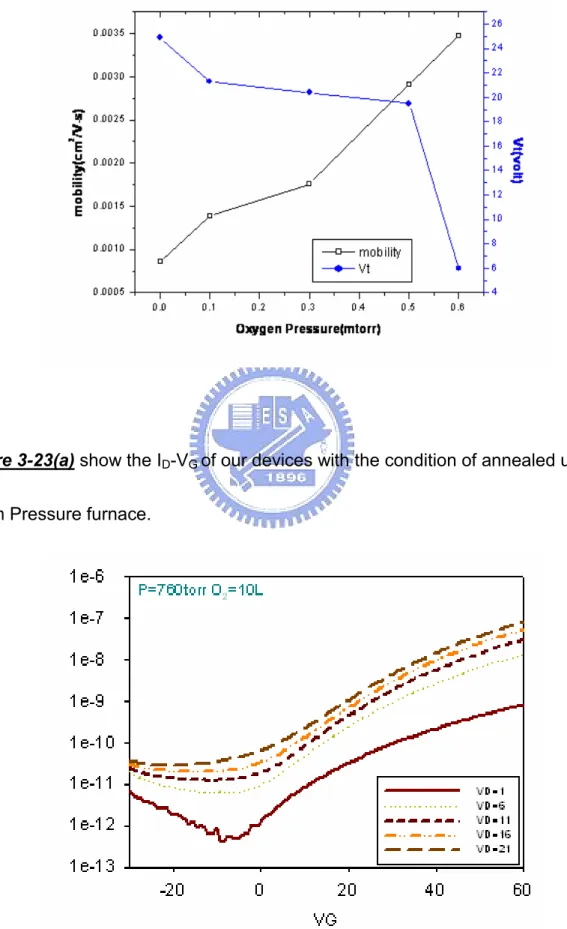
We put ZnO thin films in Vacuum Annealing Furnace at 350°C under oxygen ambient and the pressure are vacuum , 0.3 , 0.6 torr. Figure 3-15 shows the ID-VG of our devices with the condition of annealed at 350°C under oxygen ambient with pressure vacuum, 0.3 , 0.6 torr for 1 hr. Figure 3-16 shows the ID-VD of our devices with the condition of annealed at 350°C under oxygen ambient with pressure 0.6 torr for 1 hr. Figure 3-17 shows the threshold voltage and mobility of the different curing pressure.It can be seen that the threshold voltage (Vt) decreased dramatically with higher oxygen partial pressure. The mobility (µ) increased dramatically with higher
oxygen partial pressure. The maximum mobility of ZnO thin films was 4.6X10⁻³ V-1.s-1, where the pressure is 0.6 torr. The minimum threshold voltage of ZnO thin films transistor was 6 volt, where the pressure is 0.6 torr. From the electrical characteristic, we can conclude that the defect of the ZnO thin films is too much and grain size is too small at lower oxygen pressure.
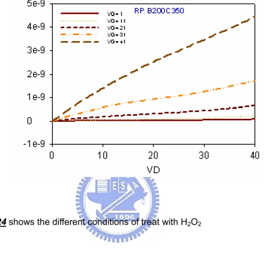
We put ZnO thin films in Room Pressure Annealing Furnace at 350°C Figure 3-18(a)(b) shows the ID-VG and ID-VD of our devices. The characteristic of ZnO TFTs is not better than annealing by Backend Vacuum Furance.
3-2-4 Hydrogen peroxide oxidation
In this chapter, we use two methods to treat with Hydrogen peroxide (H2O2). First,
we dipped the ZnO thin films transistors into Hydrogen peroxide, then we spined varied times or annealed in higher temperature. Figure 3-19 shows the different conditions of treat with H2O2. Second, we dipped the ZnO thin films transistors into
Hydrogen peroxide with different temperature.
Figure3-20 shows the ID-VG of our devices with different condition of treat with
H2O2. It can be seen that only the condition 1 showed a semiconducting characteristic,
etch the weakly bonding of ZnO. Especially, the etching phenomenon is conspicuous for grain boundary and interface of the ZnO thin films. So the other conditions show an insulator.
3-2-5 Zr
0.03Zn
9.97O based TFTs
ZnO-based TFTs reveal large off-state current, because the channel is conductive without applying gate bias. This phenomenon may be attributed to the as-deposited ZnO thin films containing high carrier densities, thus increasing the conductivity in the channel. In this paper, we replace ZnO with Zr0.03Zn9.97O.
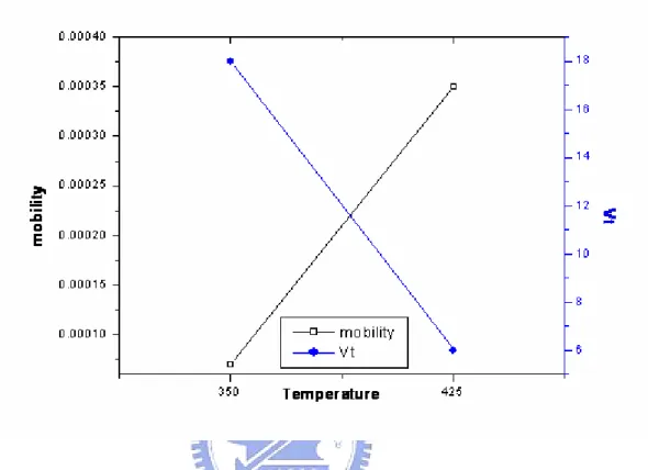
Figure3-21 shows the ID-VG and ID-VD of our devices with the condition of annealed under 0.3 torr oxygen ambient with different temperature 350 425 500°C for 1 hr. Figure 3-22 shows the threshold voltage and mobility of the different curing temperature. The threshold voltage and mobility increase with higher curing temperature. When we annealed Zr0.03Zn9.97O TFTs with 500°C for 1 hr, it shows a
normally on phenomenon. This result attribute to bigger grain size and higher carrier concentration. Figure 3-23 shows the ID-VG of our devices with the condition of annealed at 350°C under oxygen ambient with pressure vacuum, 0.3 , 0.6 torr for 1 hr. Figure 3-24 shows the threshold voltage and mobility of the different curing pressure.
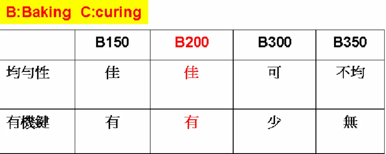
The threshold voltage decreases with higher curing temperature. The mobility increases with higher curing temperature. Figure 3-25 shows the ID-VG characteristic of ZnO and Zr0.03Zn9.97O devices. Table5 shows a comparison sheet of the ZnO and
Zr0.03Zn9.97O TFTs. The mobility and threshold voltage value of the ZnO TFTs is higher
than Zr0.03Zn9.97O TFTs. Especially, the off-current of the Zr0.03Zn9.97O TFTs is lower
Chapter 4 Conclusion
We have developed an optimized deposition condition for Sol-Gel ZnO semiconductor film and succeeded to fabricate a ZnO-based transparent thin film transistor with bottom-gate structure. The optimal conditions for depositing the ZnO film by Spin Coater at room temperature is baking 200°C on the Hotplate. With the development of wet etchants, ZnO active regions can be patterned exactly and completing TFT device fabrication. Followed by the implementation of thermal annealing at different temperature, and in different pressure with oxygen flow, the mechanism and the effect of thermal treatment on ZnO films also were studied in detail. High temperature annealing process seems to cause the high carrier concentration, and increase the conductivity dramatically. The most suitable deposition condition for ZnO films with solgel system have been successfully established by annealing ZnO at 350℃ and with 30 sccm oxygen flow at 0.6 torr. For large area flat-panel display fabrication, the chemical solution deposition process provides a more efficient way for depositing device components than vacuum techniques. Finally, We successfully demonstrated ZnO and Zr0.03Zn9.97O -based TFT
References
[1] Ü. Özgür,_ Ya. I. Alivov, C. Liu, A. Teke,_ M. A. Reshchikov, S. Doðan,_ V. Avrutin, S.-J. Cho, and H. Morkoç_ JOURNAL OF APPLIED PHYSICS 98, 041301 (2005)
[2] J. Nishii et al. “High mobility thin film transistor with transparent ZnO channels,” Jpn. J. Appl. Phys. Vol. 42, p. L347 (2003)
[3] S. Masuda et al. “Transparent thin film transistors using ZnO as an active channel layer and their electrical properties.” J. Appl. Phys. Vol.93, No.3, p.1624 (2003)
[4] Junya NISHII, Faruque M. HOSSAIN, Shingo TAKAGI, Jpn. J. Appl. Phys. Vol. 42 (2003) pp. L 347–L 349
[5] S. Walsh[ Wetch Etching fo Semiconductor Fabrication, Janus Ventures Inc.] [6] B. Schwartz, H. Robbins [J. ElectroChem Soc. 10B, 365 (1961)]
[7] Jen Hao Lee, Pang Lin, Jia Chong Ho, and Cheng Chung Lee, Electrochemical and Solid-State Letters, 9 (4) G117-G120 (2006)
[8] B J Norris, J Anderson, J F Wager and D A Keszler, J. Phys. D: Appl. Phys. 36 (2003) L105–L107
[9] Jen Hao Lee, Pang Lin, Jia Chong Ho, and Cheng Chung Lee, Electrochemical and Solid-State Letters, 9 (4) G117-G120 (2006)
[10] B J Norris, J Anderson, J F Wager and D A Keszler, J. Phys. D: Appl. Phys. 36 (2003) L105–L107
[11]Masanobu Izakia, and Junichi Katayama Journal of The Electrochemical Society, 147 (1) 210-213 (2000)
[12] R E Presley, C L Munsee, C-H Park, D Hong, J F Wager and D A Keszler J. Phys. D: Appl. Phys. 37 (2004) 2810–2813
Figure1-1 shows the hexagonal wurtize structure of Zinc Oxide
Figure2-2 shows a device structure of ZnO-TFTs
Figure3-2 illustrates the FTIR measurement result of varied baking temperature ZnO film on a single crystalline Silicon substrate
Figure3-3 illustrates the FTIR measurement result of varied Curing temperature ZnO film on a single crystalline Silicon substrate
Figure3-4 illustrates the FTIR measurement result of varied environment ZnO film on a single crystalline Silicon substrate.
Figure3-5 illustrates the FTIR measurement result of varied Curing temperature ZrZnO film on a single crystalline Silicon substrate
Figure3-6 shows the corresponding peaks of FTIR for ZrO.
Figure3-7 illustrates the SEM measurement result of the ZnO thin films anneal under 350°C oxygen environment.
Figure3-8 illustrates the SEM measurement result of the ZnO thin films anneal under 500°C oxygen environment.
Figure3-9 illustrates the SEM measurement result of the ZnO thin films anneal under 350°C vacuum environment.
Figure3-10 illustrates the AFM measurement result of the ZnO thin films baking at 150°C under oxygen environment.
Figure3-11 illustrates the AFM measurement result of the ZnO thin films baking at 200°C under oxygen environment
Figure3-12 illustrates the AFM measurement result of the ZnO thin films baking at 30°C under oxygen environment.
Figure3-14 illustrates the TDS measurement result of the Sputter ZnO thin films of capping Nitride
Figure3-15 shows the ID-VG of comparison between baking temperature150~300°C
Figure3-16 shows the ID-VD of our devices with the conditions of baking at 200°C for 10
min
Figure3-18 show the ID-VG of our devices with the condition of annealed under 0.3 torr
oxygen ambient with different temperature 350 375 400°C
Figure3-19 shows the ID-VD of our devices with the condition of annealed under 0.3
Figure 3-20 shows the ID-VG of our devices with the condition of annealed at 350°C under oxygen ambient with pressure vacuum, 0.3 , 0.6 torr for 1 hr.
Figure 3-21 shows the ID-VD of our devices with the condition of annealed at 350°C under oxygen ambient with pressure 0.6 torr for 1 hr
Figure 3-22 shows the threshold voltage and mobility of the different curing pressure.
Figure 3-23(a) show the ID-VG of our devices with the condition of annealed under
Figure 3-23(b) show the ID-VD of our devices with the condition of annealed under
Room Pressure furnace.
Figure3-25 shows the ID-VG of our devices with different condition of treat with H2O2.
Figure3-26 shows the ID-VG of our devices with the condition of annealed under 0.3 torr oxygen ambient with different temperature 350 425 500°C
Figure 3-27 shows the threshold voltage and mobility of the different curing temperature for ZrZnO TFTs
Figure 3-28shows the ID-VG of ZrZnO devices with the condition of annealed at 350°C under oxygen ambient with pressure vacuum, 0.3 , 0.6 torr
Figure 3-29 shows the threshold voltage and mobility of the different curing pressure for ZrZnO
Table 1 shows experimental flow path in my experiment.
Table 2 shows the material characteristic of the ZnO thin films with different baking conditions.
Table 3 shows electronic properties of ZnO-base TFTs with different baking conditions.
Table 4 shows electronic properties of ZnO-base TFTs with different curing conditions.
![HPSH [ 氧化數平衡反應式係數 ]](data:image/gif;base64,R0lGODlhAQABAIAAAP///wAAACH5BAEAAAAALAAAAAABAAEAAAICRAEAOw==)