國
立
交
通
大
學
光電工程研究所
博 士 論 文
新型高對比、高亮度、無轉態之 Pi-cell 液晶顯示元件
Novel High Contrast, High Brightness and Transition-Free
Pi-cell Liquid Crystal Display Device
研 究 生:陳司芬
指導教授:謝漢萍教授
新型高對比、高亮度、無轉態之 Pi-cell 液晶顯示元件
Novel High Contrast, High Brightness and Transition-Free Pi-cell
Liquid Crystal Display Device
研 究 生: 陳司芬 Student:Szu-Fen F. Chen
指導教授: 謝漢萍 博士 Advisor:Dr. Han-Ping D. Shieh
國 立 交 通 大 學
光 電 工 程 研 究 所
博 士 論 文
A Dissertation
Submitted to Institute of Electro-Optical Engineering College of Electrical and Computer Engineering
National Chiao Tung University in partial Fulfillment of the Requirements
for the Degree of Doctor of Philosophy
in
Electro-Optical Engineering January 2010
Hsinchu, Taiwan, Republic of China
新型高對比、高亮度、無轉態之 Pi-cell
液晶顯示元件
博士研究生:陳司芬 指導教授:謝漢萍 教授
國立交通大學 光電工程研究所
摘 要
薄膜電晶体液晶顯示器(TFT-LCD)技術已取代傳統 CRT 電視應用的主流。為 了使TFT-LCD 顯示技術能夠穩佔龐大的 TV 應用市場商機,TFT-LCD 開發、製 造…等相關業者無不致力於持續改善 TFT-LCD 的影像品質。由於 TFT-LCD 先天上驅動原理的限制,因此TFT-LCD 動畫顯示模糊效應(Motion blur effect)的問題
一再地被廣泛討論並尋求解決的方法。在目前所有被應用的LCD 技術中,光學
補償彎曲模態(Optically Compensated Bend, OCB;另稱為 Pi-cell)是目前反應速度 最快的向列型液晶模態,由於液晶盒(LC-cell)特殊的結構設計使它不僅具有快速
響應,同時也是具備廣視角顯示品質的液晶模態,因此在解決TFT-LCD TV 動畫
模糊效應上也是最強而有力的顯示模態。
由於 Pi-cell 快速響應的優點,使得高解析度色序法驅動的液晶顯示技術
(Field Sequential Color Liquid Crystal Display)得以有實現的可能性。然而,Pi-cell 有不同液晶形變態之間的轉換與回復(State transition and Recovery)問題,造成在 實際應用上的困難,甚至有在顯示品質最佳化上的可能性存在。本論文中,針對 此問題提出了二種新的解決方式:
得 Pi-cell 在由分散(Splay)模態轉換成彎曲(Bend)模態前必經的成核現象 (Nucleation)及完成轉態所需時間由現在的 2 分鐘(cell gap~5μm,0→6V 驅動)
縮減至少於 1 秒。使得 Pi-cell 即便是需要經過轉態過程,亦能在幾乎無法 察覺的時間內均勻地轉態完畢,且無需於瞬間外加約18 V 高脈衝電壓。 二、在前一項研究中,並不能消除 Pi-cell 的轉態特性,在顯示器的電壓操作區 間仍必須維持一個約2V 的臨界電壓以保持彎曲(Bend)模態的穩定存在。基 於液晶光學特性具有不同入射光波長的分散特性 (dispersion),紅 (R)、綠 (G)、藍(B) 三波長的電壓-透過率特性曲線(V-T curve)並不一致,因此 RGB 的臨界電壓並不相同 (VR< VG<VB)。為確保顯示器運作能維持在彎曲模態, 必須將臨界電壓維持在VB,使得Pi-cell 的透過率和對比相當程度被犧牲。
因此,我們另外提出新穎的反應型單体(reactive monomer)應用及 cell 結構設
計,使得 Pi-cell 中的液晶分子穩定在彎曲模態—驅動模態下,如此一來便 克服了Pi-cell 的轉態問題;同時,由於新結構的 cell 邊界殘留位相差值較小, 亦使得新型 RMM-Pi-cell 在不加補償膜的情況下,其靜態對比度從傳統 Pi-cell 的 26 提昇到 288 (實驗室測試樣品), 提昇度達 11 倍。 本論文在顯示應用技術領域上的貢獻在於提出以奈米結構對 Pi-cell 的液晶 配向層進行改質,以改善其轉態時間及利用反應型單体層來消除現有 Pi-cell 本 質的轉態特性,使得其所造成之光學品質缺點得以被解決或改善。而其實現方式 僅需在現有的TFT-LCD 的 Cell 製程架構中,增加 1~2 道簡單的製程,即可以完 全相容於現有的製造方式,倘若將現有的顯示器技術結合本論文研究成果將可以 創造出一種具有高影像品質的新型 Pi-cell 液晶顯示元件,使得此液晶模態的優 勢不只有應用在一般TFT-LCD,更能實現色序法驅動的液晶顯示技術。
Novel High Contrast, High Brightness and
Transition-Free Pi-cell Liquid Crystal Display Device
Doctoral Student: Szu-Fen F. Chen Advisor: Dr. Han-Ping D. Shieh
Institute of Electro-Optical Engineering National Chiao Tung University
Abstract
TFT-LCD Technology has become the mainstream in replacing CRTs in TV and other applications. In order for thin-film-transistor liquid-crystal display (TFT-LCD) technology to claim an even larger share of the TV market, manufacturers must continue to improve image quality. The issue of motion blur effect in TFT-LCD TVs has been widely discussed lately. Among the reported LC modes the Pi-cell, also known as Optically Compensated Bend (OCB) mode, has been found to be a strong candidate to reduce the motion blur effect. Due to the LC-cell structure and the driving scheme, Pi-cell is not only a wide viewing angle display technology, but also the fastest-response LCD mode among the commercialized LCD modes.
Because of the fast response of the Pi-cell, the field sequential color LCD (FSC-LCD) which displays R, G and B colors in sequence in a pixel is promising for the high-resolution display. However, Pi-cell possesses intrinsic transition and recovery issues which lead to compromised optical properties, thus, limited in its applications. In this dissertation, we proposed two modified Pi-cells to resolve these issues.
1. Proposed Nanostructure Enhanced Pi-cell (NE-Pi-cell) modified the surface of alignment layer (PI) to create nuclei for speeding up the transition rate. The transition time of a NE-Pi-cell was reduced from 2 minutes to less than 1 sec compared with the conventional one. Moreover, the transition process was uniformly completed without applying high voltage pulse (~18V).
2. Even if the previous topic could speed up the transition rate to almost zero, the critical voltage also needed to be kept over 2V for maintaining the bend state of a Pi-cell. Based on the light dispersion property of liquid crystals, the critical voltage of R, G and B were different; i.e. VR< VG< VB. In order to confirm that the Pi-cell could operate in bend state, a critical voltage larger than VB needed to be chosen, which led to compromised optical qualities. Therefore, we suggested reactive monomer modified Pi-cell (RMM-Pi-cell) to eliminate the splay-to bend state transition. Besides, because of smaller residual retardation at the dark state, the static contrast ratio of a RMM-Pi-cell, compared with conventional Pi-cell, was improved from 26 to 288 (the test samples fabricated in laboratory), up to a factor of 11 without using compensation films.
We have demonstrated a novel alignment layer modified method of a Pi-cell for uniform and fast transition without high voltage pulses. Moreover, a transition-free and high optical performance Pi-cell has also proposed in this dissertation. The proposed novel Pi-cells only need one or two simple extra processes in conventional manufacturing of TFT-LCD. Combining the research results with current high image quality LCD technology, the novel high image quality Pi-cell will be realized. The results can not only improve the image qualities for general TFT-LCD applications, but also realize the FSC-LCDs.
Acknowledgement
經過漫長的五年半,終於在這歲末年初之際完成了博士學位,對我來說至今 仍舊覺得像一場夢!當初決定回學校念博士僅僅是由於一個輕風拂面的午後,溫 暖的陽光灑在我身上,走在校園中的輕鬆感使我暫時忘卻了工作的壓力與繁忙。 然而,我沒想到的是「一個轉換心情的決定」卻讓我在人生與事業的低潮期有了 一個新的目標和重心。回想碩士畢業時那一份急於離開校門,想要快點長大的心 情,相對於在40 歲後得到博士學位而言,這次畢業不捨的感覺份外難以形容。 求學期間數度想放棄的我,因著種種因緣際會及許多人的協助與鼓勵走完了 這段看似永遠走不完的歷程。在這五年半中我首先要感謝我的指導教授—謝漢萍 院長,老師細心的指導與嚴格的要求,令我這個已經在職場許久的學生特別的感 動,畢竟在職場上不會有人再以這樣的真心來指導與糾正我的錯誤並教導我正確 做學問的態度!其次,我特別要感謝的是陳皇銘老師,雖然名義上他不是我的指 導教授,實際上在我心中他實實在在是我的指導教授,協助我完成論文當中的研 究課題,指導我論文寫作…等。 身為在職生的我,由於要身兼繁重的工作,特別感謝實驗室的學弟妹們,感 謝同為博士生的安琪、均合、柏儒、裕國和芳正為我扮演學校與我之間的橋樑, 幫我解決了不少身為在職生不能常常到校的難題。同時,我還要感謝陳皇銘老師 實驗室的學弟妹們,尤其是蓮馨、毓筠和淇文,謝謝他們對我研究課題的協助, 我能順利拿到博士學位全賴大家平時的照顧和幫忙!還有遠在美國的鄭惟中老 師,也願老師在美國一切都能順心! 最後,我想要將這份榮耀獻給我的老公、爸爸、媽媽、弟弟和妹妹們,在這 段時間內沒有他們的包容和支持我絕對走不下去。在此要特別感謝親愛的老公 Daniel 忍受我的壞脾氣,包容我不做家事,給予我實質上與精神上的雙重支持, 讓我這個身兼數職的歐巴桑能夠完成這個不可能的任務!要感謝的人實在太多 了,想要講得話怎麼樣也講不完,但是,最後我想要感謝自己、嘉許自己,多虧 自己的那份堅持,終於給了自己再開啟人生另一個可能性的機會!Table of Contents
摘 要... i
Abstract... iii
Acknowledgement ...v
Table of Contents ... vi
Figure Captions ... viii
Table List ... xi
Chapter 1 ...1
1.1 Liquid crystal displays (LCDs)...2
1.2 Motion Blur of the LCD Panel...4
1.3 FSC-LCD Application ...5
1.4 Fast Response LC Mode ...7
1.5 Motivation and objective of this thesis ...9
1.6 Organization of this thesis...11
Chapter 2 ...12
2.1 Deformation Mechanism of LC cells...12
2.1.1 Continuum Theory ...13
2.1.2 Anchoring Effect ...16
2.1.3 The Mechanical Properties of Pi-cells ...17
2.2 State Transition Scheme of a Pi-cell ...21
2.2.1 Nucleation Theory...22
2.2.2 Transition Rate ...25
2.3 Summary ...21
Chapter 3 ...28
3.1 Standard LCD Fabrication Technology ...28
3.2 Measurement Instruments...30
3.2.1 Laser Optical System ...30
3.2.2 Conoscope System ...32
3.2.3 Cell Gap Measurement -UV/Vis spectrometer LAMBDA 950 ...33
3.2.4 AFM (Atomic Force Microscope)...36
4.1 Introduction...38
4.2 The proposed Novel Nanostructure Enhanced Pi-cell ...40
4.2.1 The cell structure of a NE-Pi-cell...40
4.2.2 The Fabrication of the NE-Pi-cells...41
4.3 Nano-particle Density Investigation ...44
4.4 Transition Time v.s. Nano-particle Density ...49
4.5 Discussions ...58
4.6 Summary ...60
Chapter 5 ...61
5.1 Introduction...61
5.2 Experiments and Simulations ...63
5.2.1 RMM-Pi-cell Fabrication ...63
5.2.2 Critical Pretilt Angle Estimation ...65
5.2.3 Asymmetry Pretilt Angle Combination Simulations...67
5.3 The Investigation of RM films’ Retardations...68
5.4 The Optical Properties of Transition-Free RMM-Pi-cells ...72
5.5 Discussions ...75
5.6 Summary ...76
Chapter 6 ...77
6.1 Conclusion ...78
6.1.1 Investigation of Transition Effect in a NE-Pi-cell...78
6.1.2 Splay-to-Bend Transition-Free RMM-Pi-cell...80
6.2 Future Works...82
6.2.1 Anchoring Effect Investigation between RM Film and LC ...82
6.2.2 Fabrication Conditions Optimization of RM Films ...83
6.2.3 Manufacturing Implementation of RMM-Pi-cell into a real LCD ...84
6.2.4 Summary ...85
Reference...86
Appendix A ...93
Appendix B ...98
Appendix C ...99
Publication List ...101
Vita ...103
Figure Captions
Fig. 1-1 The various kinds of LCDs. ...2
Fig. 1-2 The cross-section view of a LCD...3
Fig. 1-3 The ON-state, OFF-state, and gray-state of one pixel on a general TFT-LCD. ...3
Fig. 1-4 The motion blur effect of the TFT-LCD driven at 60Hz frame rate...4
Fig. 1-5 The concept of the black insertion technology...5
Fig. 1-6 The normal LCD with color filters and the FSC concept. ...6
Fig. 1-7 The display mechanism of an FSC-LCD. ...6
Fig. 1-8 The cell structures and driving schemes of (a) IPS, (b) MVA, and (c) Pi-cell. 9 Fig. 2-1 Schematic drawing of (a)splay, (b)twist, (c)bend in LC cell. ...13
Fig. 2-2 Gibbs’s free energy of bend and splay states as a function of applied voltage. ...18
Fig. 2-3 Transition in Pi-cell, (a) is pretilt angle effect and (b) is the nucleation in a transition process. ...19
Fig. 2-4 Schematic diagram of two equivalent halves of a Fréedericksz cell...20
Fig. 2-5 Flow effect in Pi-cell and TN-cell...20
Fig. 2-6 The illustration of optically self-compensated property in a Pi-cell. ...20
Fig. 2-7 The commonly known states that form in Pi-cell devices. ...22
Fig. 2-8 Illustration of free energy change in nucleation process...24
Fig. 2-9 Comparison of the free energy barrier for heterogeneous and homogeneous nucleations. ...25
Fig. 2-10 Nucleation rate versus temperature, which is illustrated by diffusion limited and fluctuation rate limited...26
Fig. 3-1 Standard LCD Fabrication. ...29
Fig. 3-2 The scheme of laser optical system...31
Fig. 3-3 The schematic diagram of the measurement setup of conoscope system. ...32
Fig. 3-4 UV/Vis spectrometer LAMBDA 950 produced by Perkin Elmer. ...35
Fig. 3-5 The light pass through surface 1 and 2 whose reflective coefficients denoted as R1 and R2 causes interference. ...35
Fig. 3-6 The measuring spectrum of a test cell...36
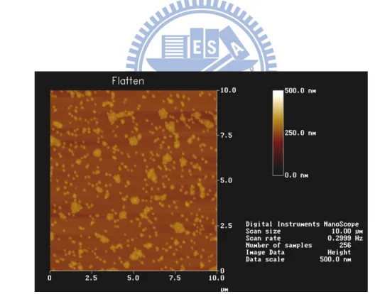
Fig. 4-1 Transition issue in Pi-cell. ...39 Fig. 4-2 The cell structure of a NE-Pi-cell...41 Fig. 4-3 NE-Pi-cell fabrication processes in laboratory...42 Fig. 4-4 0.2wt% 90nm nano-particles are coated by method 1, the particle density is
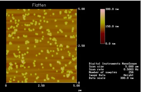
about 6.78μm-2. The aggregations are serious. ...45 Fig. 4-5 0.2wt% 90nm nano-particles are coated by method 2, the particle density is
about 11.6μm-2. The aggregation issue is improved greatly. ...46 Fig.4-6 Concentration (wt%) v.s. Density(μm-2) of 90nm nano-particles fabricated by
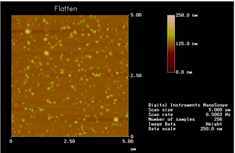
method 1 and 2, respectively. The density can be increased from 6.78 to 11.6 μm-2...46 Fig. 4-7 0.2wt% 50nm nano-particles are coated by method 2. Some aggregations
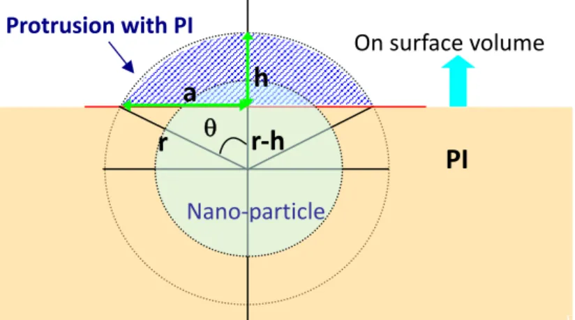
were still found when the concentration is over 0.2wt%...47 Fig. 4-8 The illustration of calculated volume of a nano-particle covered with PI on
the surface...48 Fig. 4-9 Concentration (wt%) v.s. protrusion volume ratios of the nano-particles...48 Fig. 4-10 Nucleation process of a 5 μm NE-Pi-cell. (a) Splay state, (b) Ha-to-Bend
state, (c) Bend state, and (d) Twist-to-Splay state. ...49 Fig. 4-11 The relationship between protrusion volume ratios and transition times of (a)
5μm cells (gapave. = 4.67μm), and (b) 3μm cells (gapave. = 2.8μm). ...50 Fig. 4-12 The response time of ~5μm NE-Pi-cellcells coated by nano-particles of 50
and 90nm with different nano-particle concentrations. ...53 Fig. 4-13 The response time of ~5μm NE-Pi-cellcells coated by nano-particles of 50
and 90nm with different protrusion densities. ...53 Fig. 4-14 The V-T curves of different nano-particle (50nm) concentrations with
respect to (a) 3μm cell gap, and (b) 5μm cell gap. ...55 Fig. 4-15 The V-T curves of different nano-particle (90nm) concentrations with
respect to (a) 3μm cell gap, and (b) 5μm cell gap. ...56 Fig. 4-16 The relationship between protrusion volume ratios and transition times of (a)
~5μm cells driven at 3V (Vcr ~ 2V), and (b) 3μm cells driven at 2.5V (Vcr ~ 1.7V). ...57 Fig. 4-17 (a)~(d) and (e)~(h) are the transition processes of a conventional Pi-cell and
a NE-Pi-cell, respectively. ...59 Fig. 5-1 The scheme of RMM-Pi-cell under (a) 0V and (b) 6V...62 Fig. 5-2 The relationships of film thicknesses and spin speeds of coater with respect to different concentrations of the RM solution...64 Fig. 5-3 RMM-Pi-cell fabrication processes in laboratory. ...65
Fig. 5-4 The relationship between K33/K11 and critical pretilt angle...66
Fig. 5-5 The simulations of V-T curves of two pretilt angle combinations. ...67
Fig. 5-6 The Gibbs energies of different pretilt angle combinations. ...68
Fig. 5-7 The indexs ellipsoid of the RM in diagonal frame...69
Fig. 5-8 Retardations of (a) the conventional Pi-cell, and (b) RMM-Pi-cell with different driving voltage from 0V to 6V in different viewing angles (Measuring wavelength=632.8nm)...71
Fig. 5-9 (a) The normalized RGB’s V-T curve, and (b) Un-normalized RGB’s V-T curve of RMM-Pi-cell and conventional Pi-cell without compensation films. ...73
Fig. 5-10 The improved contrast ratios of RMM-Pi-cell cells in 4.7 and 3.3 μm (Max. improved factor is 11)...74
Fig. 5-11 The Iso-Contrast Contour Diagrams of (a) Pi-cell and (b) RMM-Pi-cell. The V.A. ranges are defined by CR>10 (Measuring light source is green LED.).74 Fig. 5-12 (a) ~ (d) were the photos of a RMM-Pi-cell and (e) ~ (f) were the photos of a Pi-cell (cell gap ~ 4μm) under different driving voltages, respectively...75
Fig. 6-1 The research topics explored and concluded in this thesis...77
Fig. 6-2 The designed nano-particle treated cell structure and density upgrade of nano-particles without aggregation...78
Fig. 6-3 The photographs show the transition processes of (a) a NE-Pi-cell, and (b) a conventional Pi-cell from Ha to bend state, respectively; moreover, the (c) and (d) are with respect to the transition from twist to splay state of a NE-Pi-cell and a conventional Pi-cell...7979
Fig. 6-4 The achievements of a RMM-Pi-cell. ...80
Fig.6-5 Manufacturing Implementation of RMM-Pi-cell into an actual LCD. ...84
Fig. A-1 0.1wt% 90nm nano-particles distribution...93
Fig. A-2 0.05wt% 90nm nano-particles distribution...94
Fig. A-3 0.0125wt% 90nm nano-particles distribution...94
Fig. A-4 0.004wt% 90nm nano-particles distribution...95
Fig. A-5 0.1wt% 50nm nano-particles distribution...95
Fig. A-6 0.05wt% 50nm nano-particles distribution...96
Fig. A-7 0.0125wt% 50nm nano-particles distribution...96
Table List
Tab. 1-1 The characteristics comparisons of different LC modes ...8
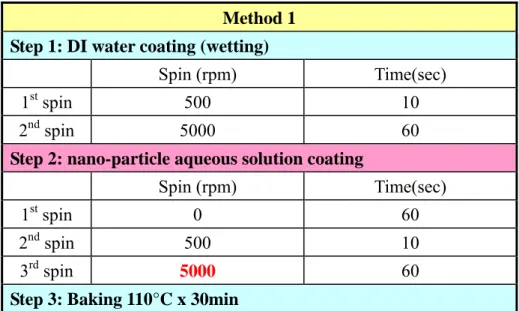
Tab. 4-1 The process condition of SiO2 nano-particle aqueous solution. ...44
Tab. 4-2 The process condition of SiO2 nano-particles + EG/PGMEA solvent...44
Tab. 4-3(a) The response time of ~5μm cells coated by 50nm nano-particles. ...51
Tab. 4-3(b) The response time of ~3μm cells coated by 50nm nano-particles...52
Tab. 4-4(a) The response time of ~5μm cells coated by 90nm nano-particles. ...52
Tab. 4-4(b) The response time of ~3μm cells coated by 90nm nano-particles...52
Tab. 5-1 The spin-coating conditions of RM films...64
Tab. 5-2 The 4wt% RMM-Pi-cells and conventional Pi-cell...70
Tab. 5-3 The pretilt angle calculations of the 4wt% RM films...70
Chapter 1
Introduction
TFT-LCD Technology has become the mainstream in replacing CRTs in all size displays and creates various hand-held display applications, as shown in Fig.1-1[1]. In order for thin-film-transistor liquid-crystal display (TFT-LCD) technology to claim an even larger share of the large display market, manufacturers must continue to improve image quality. The motion-blur artifact seen on TFT-LCDs has recently received a great deal of attention. Among the recent applications, the Pi-cell, also known as Optical Compensation Bend (OCB) mode has been found to be effective in reducing this artifact. Due to the LC-cell structure and the driving scheme, the Pi-cell so far is the fastest-response LCD mode among the commercialized LCD modes.
Since the Pi-cell has a fast response property, the field sequential color LCD (FSC-LCD) which displays R, G and B colors in sequence in a pixel is very promising for the high-resolution display as the information displays [2]. Further, FSC-LCD can be realized a high brightness display without the need of color filters which reduces the transmittance of the LCD panel by 70% (not including LC). In this dissertation, the high image quality Pi-cells will not only be designed and improved for general LCD applications but also for FSC-LCD type.
Fig. 1-1 The various kinds of LCDs [1].
1.1 Liquid crystal displays (LCDs)
A cross-section of an LCD, as shown as Fig. 1-2, reveals its elements. The LC cell is at the center of the display where the liquid crystal is located. Transparent electrodes patterned on each pane of glass encompass the liquid crystal. Light passes through a bottom polarizer that orients the light to a single state of polarization by absorbing over 50% of the incoming unpolarized light. The orientation of the liquid crystals can be changed by applying a voltage to the electrodes in order to change the level of illumination displayed in each sub-pixel. However, if a voltage is applied, the liquid crystals align to the electric field and do not rotate the light, allowing the top polarizer to block it completely. By applying an intermediate voltage, the liquid crystal can be partially oriented to control the transmittance of the incoming light, creating shades of gray as shown in Fig. 1-3. Adding a color filter to the LCD panel creates color displays. In a color LCD, each red, green and blue sub-pixel is individually controlled, allowing varying amounts of red, green, and blue light through to the viewer for each pixel.
Rear Polarizer Front Polarizer TFT device Sealant Blacklight Unit Liquid crystal Color filter Glass Glass Rear Polarizer Front Polarizer TFT device Sealant Blacklight Unit Liquid crystal Color filter Glass Glass
Fig. 1-2 The cross-section view of a LCD.
Source: Dr. Chun-Ho Chen’s dissertation for Ph. D in NCTU, 2009. Fig. 1-3 The ON-state, OFF-state, and gray-state of one pixel on a general TFT-LCD.
1.2 Motion Blur of the LCD Panel
Due to the TFT-LCD driving scheme, the sub-pixels of a LCD panel are driven by hold-type square function. When the object displayed on the TFT-LCD moves fast as in sports, the edge of the object image will become blurred with multiple images, shown in Fig. 1-4. The motion quality of LCD TVs is evaluated by using the well-known figure of merit — VESA’s Moving Picture Response Time (MPRT).
Fig.1-4 The motion blur effect of the TFT-LCD driven at 60Hz frame rate.
In order to improve the motion quality of a TFT-LCD, the impulse driving scheme on TFT-pixels, simulates the CRT’s impulse type light emission, has been adopted. There are many approaches in recently proposed technologies; the simplest one is Black Insertion (BI) whose driving scheme is shown in Fig.1-5. By using BI technology, which can alternate between a black data frame and a display data frame,
6 600HHzz M MPPRRTT~~1188mmss((MMVVAA)) pixels time Blur edge 60Hz sec 60 1
the MPRT of a general TFT-LCD TV can approach 12ms; yet, the MPRT of a CRT is 4ms. However, the result can not be satisfied with image quality, because the MPRT is still larger than CRT’s and the brightness of a LCD needs to be compromised. According to the various proposed technologies such as black data insertion, black frame insertion, scanning backlight and 120 Hz Motion Estimation Motion Compensation (MEMC) applications, a double frame rate to drive the LC panel is needed for these improving methods. Therefore, the fast response LC mode is a key requirement for motion blur improvement. Among all of LC modes, the Pi-cell is a strong candidate in commercialized LCD modes [3] for resolving the motion blur issue.
Fig. 1-5 The concept of the black insertion technology.
1.3 FSC-LCD Application
A TFT-LCD system is commonly illuminated by a constant full-on conventional CCFL backlight. The generated light propagates through two sets of polarizers, color filters, diffusers and redirection foils, and in each of these components, substantial
proportions of light are scattered and absorbed. Overall, the efficiency of the above optical stack amounts to approximately 5-10%.
Time
Colored Sub-pixels
Monochrome Pixel =3 x Sub-pixel White Backlight Colored Backlight
Normal LCD--Spatial Colored FSC-LCD--Temporal Colored
1 frame = 1 field Frame rate = 60 Hz 1 frame = 3 field Field rate = 180 Hz Time Colored Sub-pixels Monochrome Pixel =3 x Sub-pixel White Backlight Colored Backlight
Normal LCD--Spatial Colored FSC-LCD--Temporal Colored
1 frame = 1 field Frame rate = 60 Hz
1 frame = 3 field Field rate = 180 Hz
Fig. 1-6 The normal LCD with color filters and the FSC concept.
Time
full color image
Red Green Blue
5.56 ms 1 Frame: 1/60 Sec ~16.7 ms Data Load LC Set LED Flash Data Load LED Flash Data Load LC Set LED Flash LC Set
Fig. 1-7 The display mechanism of an FSC-LCD.
Most LCDs rely on spatial color synthesis to produce vivid saturated color images by juxtaposing strip color-filter (typically RGB) sub-pixels. However, color filters absorb roughly 70% of light and are therefore highly inefficient. To significantly improve LCD power efficiency, it is therefore appealing to remove the color filters and rely on temporal color synthesis to create full-color images. The display concepts of a conventional TFT-LCD and a FSC-LCD are shown in Fig. 1-6. Such FSC-LCDs rapidly flash the three primary colors time-sequentially, as illustrated in Fig. 1-7, such that the colors are mixed by means of temporal integration in the
eyes and all three colors seem present simultaneously [1][4-8]. Colored LEDs are an ideal light source for this mode of illumination. To prevent luminance flicker, a three-primary system requires a minimum refresh rate of 180 Hz. In other words, FSC-LCD technology also needs a sufficiently fast response LC mode.
1.4 Fast Response LC Mode
Three kinds of LCD modes are currently in the mainstream of the LCD industry. They are multi-domain vertically aligned (MVA) [9], in-plane switching (IPS) [10], and optically compensated bend (OCB) [11] mode LCDs, whose cell structures and driving concepts are shown in Fig. 1-8. Their distinguished feature of “wide viewing angle” is an important requirement for LCD-TV applications. Therefore, these three wide-viewing LC modes are selected to develop the further fast-switching requirement.
Though IPS and MVA modes have very outstanding wide-viewing characteristic, their response times are not fast enough for high-frame-rate display applications, such as field sequential color LCD or temporally multiplexing 3D display. Therefore, a novel technique, Pi-cell also known as OCB mode, was proposed to fulfill these requirements. The comparisons of different LC modes are listed in Tab. 1-1. Though OCB-LCD is regarded as the fastest switching LCD mode among the LCDs, some issues still need to be resolved. Among them, the most critical issue is the recovery from the bend state back to the splay or twist states.
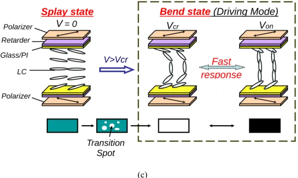
As shown in Fig. 1-8 (c), the Pi-cell is normally operated in the bend state; however, because of the topological difference between the ground splay state and the bend state, a nucleation transition has to be completed before operation. The transition
can be initiated by applying a critical voltage (Vcr), and then this voltage is held to sustain the device in the bend state. However, the Pi-cell still has the tendency of relaxing into the splay state. Therefore, we will propose two novel Pi-cell structures to resolve transition issue: one is to form a nanostructure by coating nano-particles before PI treatment to enhance the transition rate from splay to bend state; the other one is to use reactive monomers to modify the pretilt angle of alignment layer whose anchoring energy may be changed for the contrast ratio improvement.
Tab. 1-1 The characteristics comparisons of different LC modes. (Data source: Chung Hwa Picture Tube, LTD)
◎ ○ ○ ◎ Fabrication ◎ ○ ◎ △ Viewing angle △ (600:1) ◎ (1200:1) ○ (800:1) △ (600:1) Intrinsic Contrast Ratio ◎ (<3) △ (~20) △ (~20) ○ (~12) Intrinsic Response (ms) ○ (state transition) ◎ ◎ ◎ Driving Pi-cell MVA IPS TN Items ◎ ○ ○ ◎ Fabrication ◎ ○ ◎ △ Viewing angle △ (600:1) ◎ (1200:1) ○ (800:1) △ (600:1) Intrinsic Contrast Ratio ◎ (<3) △ (~20) △ (~20) ○ (~12) Intrinsic Response (ms) ○ (state transition) ◎ ◎ ◎ Driving Pi-cell MVA IPS TN Items
◎: Excellent ○: Good △: Acceptable X: Poor
(c)
Fig. 1-8 The cell structures and driving schemes of (a) IPS, (b) MVA, and (c) Pi-cell.
1.5 Motivation and objective of this dissertation
With the growth of the information industry, the display technique requirements have become increasingly demanding. The desirable features are high contrast ratio, high power efficiency, high resolution and good visual quality. To fulfill these features, we designed and demonstrated the new technologies to achieve high contrast ratio and clear motion image quality. We did this by using conventional Pi-cell, also named OCB mode, in the OCB-LCD TV. To evaluate the motion quality of LCD TVs, we used the Moving Picture Response Time (MPRT). By applying the Dynamic Scanning Backlight with Black Insertion (DSBBI) technology previous proposed by our research team, the MPRT of a 32-inch OCB-LCD TV can achieve 5.9 ms in average gray-to-gray levels, which is comparable to CRT TV (MPRT~4ms) but better than other LCD modes [12]. By changing the structure of the LC cell, the contrast ratio of OCB-LCD TVs can be improved by 60% by adjusting the gamma curves with respect to R, G and B individually. With dynamic controlled backlight luminance, the contrast
V>Vcr Transition Spot
Splay state
Polarizer Retarder Glass/PI LCV
= 0 PolarizerBend state
(Driving Mode)
V
crV
onFast
response
ratio of OCB-LCD TVs can even achieve greater than 1000:1 at 50% dimming setting [3].
To further realize the features of high power efficiency, adopting the FSC-LCD structure is a good candidate. The requisite components of FSC-LCD are the fast switching modes of liquid crystal and the backlight module. Among these requirements, the most urgent one is the fast response LC mode because the current research in the field is still short of realizing the FSC-LCD without the color break-up (CBU) phenomenon. The OCB-LCD modes possess the possibility to achieve the FSC-LCD.
In the demonstration of a 32-inch OCB-LCD TV, using conventional Pi-cell, we found two key issues that need to be resolved. First, applying the critical voltage bias for the LC state transition from splay state to bend state and keeping it in stable bend state are strict. To hold the Pi-cell in stable bend state, the applied voltage should be larger than the critical voltage of blue light. As the result, the transmittance and contrast ratio of the Pi-cell must be degraded. Therefore, it is necessary to develop a novel Pi-cell that is stable in bend state without bias voltage [13]. Second, in order to obtain good dark state and wide viewing angles in all viewing directions, we used commercial OCB-WV films to compensate for the viewing angle dependence of bend alignment LC cell [14]. However, the retardation mismatch occurs when the OCB-LCD shows the low gray-level images or patterns at large viewing angles and results in the red and blue light leakages corresponding to the right and left sides of rubbing direction respectively. Therefore, to design a high contrast ratio and transmittance of Pi-cells without using OCB-WV films is a challenge. In order to realize high image quality displays which fulfill the aforementioned features, it is very important to find the solutions to the two key issues mentioned above.
In this dissertation, I will describe the tasks completed on the aspects of the Pi-cell and the future works for performance improvements.
1.6 Organization of this dissertation
This dissertation is organized as follows: the principle of deformation mechanism of LC cells, the mechanical properties and transition scheme of a Pi-cell are presented in Chapter 2. The continuum theory, anchoring effect, homogeneous and heterogeneous nucleation theory are described. Additionally, this chapter also presents the operation principle and special characteristics of a Pi-cell. In Chapter 3, the standard TFT-LCD fabrication processes are introduced. And the instruments used in experiment for optical property measurements are described. The basic measuring concept and set-up of the measurement systems are also described in details. In
Chapter 4, the novel nanostructure enhanced Pi-cell (NE-Pi-cell) is proposed. The
fabrication methods of nanostructures are investigated and optimized; the limitation of nano-particle density is also analyzed. In addition, the dynamic observations and transition rate of a conventional Pi-cell and proposed NE-Pi-cell are presented and evaluated. In Chapter 5, the transition-free RMM-Pi-cell is proposed. The novel structure and the fabrications of a RMM-Pi-cell are presented. The performance comparisons between a conventional Pi-cell and a RMM-Pi-cell are investigated. The potential issue of the RMM-Pi-cell is also discussed here. Finally, the summary of the dissertation and future works are given in Chapter 6.
Chapter 2
Theory and Principle
The deformation mechanism of a LC cell and the principle of state transitions in a Pi-cell are introduced. The continuum theory is used to calculate the Gibbs’s energy of a certain state, and Rapini-Papoular approach is used to calculate the alignment effect on the orientation of LC director. In the principle of state transitions in a Pi-cell, the well-known nucleation theory method is illustrated. In order to study the rate of state transitions, we propose hetero-nucleation theory to explain why the heterogeneous surface energy status can shorten the transition time in a Pi-cell.
2.1 Deformation Mechanism of LC cells
In LCDs, an electric field is often applied to cause reorientation of the LC molecules. The switching performance of an LC device relies on its cell structure design. The Ossen-Frank continuum theory [15-18] is well-used by the LCD researchers. A basic continuum theory considers that the elastic constants of LC molecules determine the restoring torques arise when the system is perturbed from its equilibrium configuration. It is the balance between the electric torque and the elastic restoring torque that determines the LC’s static deformation pattern. Taking more factors into consideration, such as the electric field, the magnetic field, and the anchoring effect makes the equation more appropriate to the actual LCD cases. The detailed description of continuum theory is explained as follows.
2.1.1 Continuum Theory
The Ossen-Frank continuum theory is well-known for the calculation of the equilibrium configuration of LC directors in a cell. LCs exhibit curvature elasticity. When an electric filed is applied to an LCD device, the LC molecules will be reoriented. The electric torque needs to be balanced by elastic restoring torque determines the LC’s deformation pattern. Any static deformation of LCs can be divided into a combination of three basic deformations: splay, twist, and bend, as illustrated in Fig. 2-1.
Fig. 2-1 Schematic drawing of (a)splay, (b)twist, (c)bend in LC cell [19].
We consider a nematic LC cell in the xy plane. The z axis is chosen to be perpendicular to the cell, so that the cell is located between z = 0 and z = d. Initially, the LC molecules are aligned parallel to the xy plane. An electric field is applied in the LC cell. Following the notation of Ossen-Frank continuum theory, the energy densities of a deformed LC and the electromagnetic field can be written as Eq. (2-1) [20].
[
]
( ) 2 1 ) ( ) ( ) ( 2 1 2 33 2 22 2 11 ∇⋅n + n⋅∇×n + n×∇×n − E⋅D = k k k F (2-1) 0 ≠ ⋅ ∇ n n⋅∇×n≠0 n×∇×n≠0where k11, k22, and k33 are the splay, twist and bend elastic constants, respectively and
n is the unit vector representing the director distribution in the cell. The elastic
constants are strongly temperature dependent. E is the applied electric field and D is the displacement field vector.
Consider twist and tilt mode. The director n is uniformity twisted as a function of z, so the initial director distribution can be expressed,
) 0 , sin , (cosφ φ = n (2-2)
A uniform electric field is applied along the z axis. As a result, the directors are tilted toward the direction of the electric field. This leads to redistribution of the director n as a function of z. Therefore, the director can be written,
) sin , sin cos , cos (cosθ φ θ φ θ = n (2-3)
where (θ, φ) are the positioned angles of the LC director, denote the polar coordinates rotated about y axis by θ and about z axis by φ. Substituting Eq. (2-3) to Eq. (2-1), the elastic energy density is obtained as:
[
]
[
]
2 2 2 33 2 22 2 2 33 211 cos sin cos
2 1 sin cos 2 1 ⎟ ⎠ ⎞ ⎜ ⎝ ⎛ × + + ⎟ ⎠ ⎞ ⎜ ⎝ ⎛ + = dz d k k dz d k k UEL θ θ θ θ θ θ φ (2-4)
The electromagnetic energy density term is
D E⋅ = 2 1 EM U (2-5)
Actually, we are care about the change of the electromagnetic energy density due to the change of the dielectric constant ε as the LC director distribution changes.
Considering the first case: a constant voltage, the electric field E is a constant (E=V/d), regardless the magnitude of the dielectric constant. The net change of the
electromagnetic energy density due to a change of the dielectric constant can be written as: 2 0 2 2 1 2 1 E Ad Q V E UEM = ε − Δ − ε Δ (2-6) where A is the area of electrodes, d is the separation between the electrodes, and ΔQ is additional charges supplied by power supply. It can be denoted by
d V E d V A Q= − = Δ (ε ε0) , (2-7) Substituting Eq. (2-7) into Eq. (2-6), we obtain
2 2 0 2 1 2 1 E E UEM = ε − ε Δ (2-8) where ε0 is the initial dielectric constant. A larger final dielectric ε leads to a lower energy density.
Considering another general case, the surface charge density is constant. Therefore, the displacement field D is a constant. The change of electromagnetic energy density due to a change of dielectric constant can be written
0 2 2 2 1 2 1 ε ε D D UEM = − Δ (2-9) We postulate the LC cell is uniform in xy plane, and the electric field E is applied along z axis. An application of Maxwell’s equation and the boundary condition on the surface lead to:
0 = = y
x E
E (2-10)
(
⊥)
⊥ − + = Δ ε θ ε θ ε 2 2 2 || 2 2 1 cos sin 2 1 Z Z EM D D U (2-11)where ε⊥ is the initial dielectric constant, DZ (=constant) is the z component of the displacement field vector. The second term is a constant independent of the director orientation θ(z). And the component DZ can be written
E DZ ( cos sin2 ) || 2θ ε θ ε + = ⊥ (2-12) The total free energy in the cell is given by
(
)
(
)
[
θ θ]
θ θ θ ε θ ε θ ε φ θ 2 2 33 2 22 2 2 33 2 11 1 0 2 2 2 || 2 2 2 2 1 0 cos sin cos sin cos where cos sin 2 1 k k F k k F dz D D dz d F dz d F dz U U U d Z Z d EM EL + = + = ⎥ ⎥ ⎦ ⎤ ⎢ ⎢ ⎣ ⎡ − + + ⎟ ⎠ ⎞ ⎜ ⎝ ⎛ + ⎟ ⎠ ⎞ ⎜ ⎝ ⎛ = Δ + =∫
∫
⊥ ⊥ (2-13)The preferred LC director distribution functions θ(z) and φ(z) can be acquired by minimizing the total free energy using variation method. i.e. Let δU=0 and give suitable boundary conditions, then the Umin. can be obtained at the same time.
2.1.2 Anchoring Effect
The LC alignment affects the equilibrium state, switching property, and director configuration of an LC cell. This alignment is generally achieved by the anchoring effect with a pretreated layer. Most preferably, polyimide is used owing to its low cost, high stability, and easy process. Two major methods are used to pre-treat the alignment material: mechanical rubbing and photo-alignment. The mechanical rubbing method is executed by a roller covered with woolen texture. By brushing in the same direction, the alignment layer is strained, and this strain aligns the LC
director in a certain direction. The other method of pre-treating the alignment material is to use polarized UV light to orient the molecules of alignment layer in a certain direction. This method can be used along with a photo-mask to make multi-directional alignments in one substrate, but the uniformity is still an issue.
This stabilization mechanism can be expressed by Rapini-Papoular approach [21-23] as follows: φ θ F F Fs = + (2-14) ) ( sin 2 1 0 2 θ θ θ θ = W − F (2-15) ) ( sin 2 1 0 2 φ φ φ φ = W − F (2-16)
where θ and φ denote the polar and azimuthal angles, Fs denotes the total free energy
resulting from the anchoring effect, Fθ denotes the free energy component in terms of the polar angle, Fφ denotes the free energy component in terms of the azimuthal angle. Wθ and Wφ are the constants denote the interactions between the substrates and the LC directors. θ0 and φ0 are the equilibrium angles with respect to the polar and azimuthal dimensions.
Considering the anchoring effect, the continuum equation mentioned in 2.1.1 needs to be modified as follows. The orientation distribution of stabilized LC directors of a LC cell can be illustrated by the equation.
[
k k k]
Fs F = ∇⋅ + ⋅∇× + ×∇× − ( ⋅ )+ 2 1 ) ( ) ( ) ( 2 1 2 33 2 22 2 11 n n n n n E D (2-17)2.1.3 The Mechanical Properties of Pi-cells
(π) from surface to surface when the Pi-cell is in operation. The alignment arrangements of upper and lower substrates in a Pi-cell are parallel. Generally, the initial state of a Pi-cell prefers to be aligned in splay state. By calculating the Gibbs’s free energy in Eq. (2-17), the stable state corresponding to the applied voltage can be obtained. As shown in Fig. 2-2, the cell is more stable in splay state than in bend state without applying a voltage. While applying a voltage larger than critical voltage, the bend state becomes more stable than the splay state [24-26].
Source: T. Uchida et al., SID’00 Digest 31, 26 (2000).
Fig. 2-2 Gibbs’s free energy of bend and splay states as a function of applied voltage [24].
Take the pretilt angle into account; the Gibbs’s free energy diagram can be used to determine the pretilt angle of a Pi-cell which is in the bend state initially. As shown in Fig. 2-3 (a), if the pretilt angle is much lower than critical pretilt angle, the Gibbs’s free energy of the bend state is too large to be stabilized. In other words, if the pretilt angle is higher than critical pretilt angle, the bend state can be stabilized without applying a voltage. In heterogeneous case, the bend state can be initiated with nucleation by applying a voltage, as shown in Fig. 2-3 (b) [11][24][27-30].
Source: T. Uchida et al., SID’00 Digest 31, 26 (2000).
Fig. 2-3 Transition in Pi-cell, (a) is pretilt angle effect and (b) is the nucleation in a transition process [24][27].
Furthermore, the Pi-cell has the rapid response time because the cell is operated between the bend state at the critical voltage (Vcr) and the near homeotropic state at high voltage. The symmetric director configurations in the lower and upper parts of the LC layer, regarded as two halves of a Fréedericksz cell, imply the equivalent cell gap is one half of the real LC layer. Because the response time of a LC cell is proportional to the square of cell gap, the response time of a Pi-cell has improved by a factor of four.. The schematic diagram is shown in Fig. 2-4. Besides, the flow effect of a Pi-cell leads to the response time improvement is more than four times. The LC flow in Pi-cell is toward the same direction; therefore, the backflow effect can be ignored. The comparison of the flow effect in a Pi-cell and the anti-parallel backflow, which slows down the response of LCs, in a TN-cell is shown in Fig.2-5.
In addition to fast response, the optically self-compensated property is also a key design factor in a Pi-cell. Due to the symmetric director configurations of a Pi-cell, the optical retardations are almost the same, no matter people see from left or right sides, as shown in Fig. 2-6. Therefore, Pi-cell is a kind of wide viewing angle technologies.
Critical pretilt angle
Fig. 2-4 Schematic diagram of two equivalent halves of a Fréedericksz cell.
Fig. 2-5 Flow effect in Pi-cell and TN-cell.
Fig. 2-6 The illustration of optically self-compensated property in a Pi-cell.
Pi-cell TN-cell
Long axis Short axis
2.2 State Transition Scheme of a Pi-cell
Pi-cell [31] possesses fast response time, due to lacking of backflow during molecular relaxation [32-36] in its bend state, for liquid crystal display (LCD) application. Generally, the Pi-cell is operated in the bend state; a nucleation transition has to be completed to operate the Pi-cell in the bend state. The Pi-cell, however, has five distinct states in its transitions, illustrated in Fig.2-7. There are (1) the splay ground state, (2) the symmetric splay state (Hs), (3) the asymmetric splay state (Ha), (4) the bend state, and (5) the 180° twist state [37-39]. The lowest free energy state is splay state without an applied voltage. When applied a voltage higher than the first critical voltage VC1, Hs state would be formed under the same surface condition on both sides of a Pi-cell. The Hs state, then, quickly turned into asymmetric Ha state. As the applied voltage was further increased beyond the second critical voltage VC2, also called the critical voltage, denoted Vcr, of a Pi-cell, the bend state became the stable state. The voltage had to be kept larger than the critical voltage to sustain the cell in the bend state; otherwise, the LC molecules would be relaxed into twist or splay states in a Pi-cell. In TFT-LCD applications, due to the limitation of the maximum driving voltage ( ~ 6V) and the requirement of sustained voltage to prevent recovery of the splay state, the Pi-cell is generally driven in the range between 2 ~ 6V [40]. In the transition scheme, there are two nucleation processes included; one is Hs (or Ha)-to-bend state, the other one is bend state relaxed into twist state.
Fig.2-7 The commonly known states form in Pi-cell devices [41].
2.2.1 Nucleation Theory
Classical nucleation is the extremely localized budding of a distinct thermodynamic phase. Some examples of phases that may form via nucleation in liquids are gaseous bubbles, crystals, or glassy regions. Nucleation generally occurs with much more difficulty in the interior of a uniform substance, by a process called homogeneous nucleation. The creation of a nucleus implies the formation of an interface at the boundaries of a new phase. As mentioned above, the splay-to-bend transition in a Pi-cell has to be completed via so-called nucleation process. In the process, an interface forms to be the boundary between splay and bend states. When the extra voltage, higher than the critical voltage, is applied to the Pi-cell, the extra driving power will force for nucleation and bring about a change in free energy per unit volume, Gv, between splay and bend states. This change in free energy is
balanced by the energy gain of creating a new volume, and the energy cost due to
Splayed ground state V>Vc1 Symmetric H state Glass Polyimide Asymmetric H state Bend state Twist state V>Vc2 Nucleation ITO V<Vc2 Nucleation Operation state V Bright Dark
creation of a new interface. When the overall change in free energy, ΔG is negative, nucleation is favored.
Some energy is consumed to form an interface, based on the surface energy of each phase. If a hypothetical nucleus is too small (known as an unstable nucleus or "embryo"), the energy that would be released by forming its volume is not enough to create its surface, and nucleation does not proceed. The critical nucleus size can be denoted by its radius, and it is when r = r* (or r critical) that the nucleation proceeds.
In the classic case [42] of a spherical cluster that liberates -Gv J/cm3 during
formation (here Gv is a negative quantity), but which must pay the positive cost of σ
J/cm2 of surface interfacing with the world around, the free energy needed to form a cluster of radius r is σ π π 3 4 2 3 4 r G r G= v+ Δ (2-18) where the first term shows the energy gain of creating a new volume and the second term shows the energy loss due to surface tension of the new interface. It costs free
energy to add molecules to this cluster (because >0 dr dG
) until the radius reaches to
the critical value,
v G
r*=−2σ . And we can find the free energy needed to form the
critical radius by 23 3 16 * v G G = πσ
Δ , which is the maximum ΔG (where =0
dr dG
). The
Source: http://en.wikipedia.org/wiki/Nucleation
Fig. 2-8 Illustration of free energy change in nucleation process [44].
As mentioned above, homogeneous nucleation occurs with much difficulty. Actually, another nucleation type, called heterogeneous nucleation, occurs much more often than homogeneous nucleation. It forms at preferential sites such as phase boundaries, defects or impurities like dust and requires less energy to than homogeneous nucleation. At the preferential sites, the effective surface energy is lower, thus diminished the free energy barrier and facilitating nucleation. Surfaces promote nucleation because contact angles greater than zero between phases encourage particles to nucleation. In splay-to bend-transition case we studied, at the specially created preferential sites, the free energy needed for heterogeneous nucleation is equal to the product of homogeneous nucleation and a function of contact angle, which results the barrier energy needed for heterogeneous nucleation reduced.
) (
hom f θ
G
Gheterogeneous =Δ ogeneous∗
Δ (2-19) Where θ θ cos3θ 4 1 cos 4 3 2 1 ) ( = − +
f , θ is limited in the range between 0 and π.
The illustration of difference between homogeneous and heterogeneous nucleations in energy barriers is shown in Fig. 2-9.
Source: http://en.wikipedia.org/wiki/Nucleation
Fig. 2-9 Comparison of the free energy barrier for heterogeneous and homogeneous nucleations [44].
The barrier energy needed for heterogeneous nucleation is reduced, but the critical radius remains unchanged. In other words, the heterogeneous surfaces increase the change of the strain energy density included in Gibbs free energy density (i.e. negative quantity becomes larger.) [44-45]. The transition process of a Pi-cell, the uniform distribution of nano-particles will affect the rate, uniformity, and strength of the transition.
2.2.2 Transition Rate
The transition rate in Pi-cell is positively correlated with nucleation rate per
unit volume. The relationship is shown as following equation [44].
t T k G N I B Δ ∝ Δ − ∝ ν exp( ∗) 1 (2-19) Where ΔG* is free energy barrier (ΔG* >0). ν is the attempt frequency; N is the number of potential nucleation sites per unit volume; kBis the Boltzmann constant and Δt is transition time. The transition rate depends on the attempt frequency, the number density of nucleation sites and probability of successful attempts. The smaller ΔG*
and the larger N are, the larger transition rate is.
The number of nucleuses of a certain size formed is a function of the total number of atoms in the system, the free energy to create a nucleus of that size, and the temperature. The number of nucleuses increases with increasing temperature. As temperature (significantly below melting temperature or Tni, which is nematic- isotropic transition temperature.) increases, molecules are able to get to the site of nucleation at a fast enough rate to promote the growth of the nucleus. Therefore, nucleation rate is dominated by the diffusion. However, as temperature increases, the fluctuations of molecules increase and molecules tend to escape from the nucleus, resulting in a decrease of nucleation rate [45-46].
Source: http://en.wikipedia.org/wiki/Nucleation
Fig. 2-10 Nucleation rate versus temperature, which is illustrated by diffusion limited and fluctuation rate limited [44].
In the transition process of a Pi-cell, the transition time measurement is often kept at room temperature. Therefore, the thermal dynamic behavior was not discussed in the study. The study was focused on the nucleation rate (or transition rate) increased by the heterogeneous surfaces.
2.3 Summary
In chapter 2, the continuum theory was used to calculate the Gibb’s energy of the LC profiles, and the nucleation theory was used to explain the transition processes in a Pi-cell, were illustrated. From the chapter, we could realize the driving behaviors of a Pi-cell and know how to resolve the transition processes in a Pi-cell. If we wanted to resolve the transition issue, we needed a higher pretilt angle at the cell boundary to change the equilibrium LC profiles in a Pi-cell or a heterogeneous nucleation to enhance the transition rate. According to these studies, we then proceeded two research objectives to resolve the transition issue in the dissertation.
Chapter 3
Device Fabrication and Measurement
The standard fabrication technologies of LCD are described. These fabrications will be used to make our designed devices. After the devices and special treatment substrates being fabricated, the cell characterizations of the optical performance, iso-contrast diagram and cell gap are measured with the Laser optical system assembled by our laboratory, Conoscope system and UV/Vis spectrometer LAMBDA
950 made by PerkinElmer, respectively. Then, the morphologies of the nano-particle
coated substrates and RM films’ thicknesses are investigated by Atomic Force
Microscope (AFM).
3.1 Standard LCD Fabrication Technology
A LCD device is fabricated by stacking two substrates with intermediate liquid crystal. The standard fabrication technology of a LC cell is shown in Fig. 3-1. Two substrates need to be prepared in advance; one substrate is formed well-known thin film transistors (TFT) to be a pixel array, and another one substrate is fabricated by color filter (CF) processes for color separation. In general, the standard a-Si TFT fabrication needs five sequential masks for photolithography processes include film depositing, UV exposure, developing, etching, and photoresist striping; CF fabrication needs at least four sequences of masks to form BM, R, G and B. Two prepared substrates have to be treated individually by polyimide (PI) with textile buffed for LC alignment before assembling them. After that, the spacers are sprayed on TFT
substrate to sustain the cell gap and sealant is dispensed on CF for cell assembling. Then, the assembled empty cell is filled in LCs and attached polarizers. Finally, the external ICs and Flexible Printed Circuit (FPC) are bonded to complete an LCD device [47].
3.2 Measurement Instruments
3.2.1 Laser Optical System
The laser optical system shown in Fig.3-2 was used to measure the electro-optic characteristics of the LC cells. The major measurements include Voltage versus Transmittance, retardations, and response time.
We set three lasers for R, G and B whose wavelengths are 632.8, 532 and 473nm, respectively as the measuring light sources. After putting the LC cell between polarizer and analyzer, the laser light passes through 10% ND filter first to degrade the intensity into an acceptable range for photo-detector; then the laser travels through the polarizer, cell, analyzer, and finally to the photo-detector. When the laser light passes through the LC cell, the light is modulated with the phase change of 2πΔnd/λ which changes the light intensity received by the photo-detector.
The LC cell is driven by WFG500 (company: FLC Electronics AB), which is a multi-channel high voltage waveform generator whose maximum output voltage range is ±100V and the minimum designable pulse width is 200ns, connected with PC through GPIB interface. The driving waveform applied to the cell is 1k Hz square wave for the voltage versus transmittance measurement. The photo-detector PIN20 (company: FLC Electronics AB) detects and transforms the output light intensity from analyzer with response more than 40ns into voltage. Then, the oscilloscope (company: Tektronix) and the multi-muter (company: Keithley) exhibit and transfer the output signals to the PC.
When measuring the retardations of the cell, a compensator (Soleil-Babinet, From Special Optics, Model: 8-400-UNCOATED) is positioned in between polarizer
and analyzer, illustrated as Fig.3-2. First, to rotate the compensator and record the two minimum signals detected by photo-detector, denote the two signals as min.1and min.2 without inserting the LC cell.
Fig.3-2 The scheme of laser optical system.
After the cell positioning between polarizer and compensator, we have to rotate the compensator and record the minimum signal denoted as x. The retardation angle is calculated by Eq. (3-1). *360 2 . min 1 . min 2 . min ⎟ ⎠ ⎞ ⎜ ⎝ ⎛ − − = Γ = x Angle n Retardatio (3-1)
Following the result calculated by Eq. (3-1), the retardation value is derived as Eq. (3-2). 360 * nd=Γ λ Δ = Value n Retardatio (3-2) R G,B Light source
polarizer Compensator analyzer LC cell Adjustab Waveform Generator ND Filter Multi-meter Data Output Waveform Input Signal Input Signal Input Data Output Data Output Photo-detector Data Output Oscilloscope
3.2.2 Conoscope System
The conoscopic instrument (Autronics-Melchers GmbH) is used for measuring the optical properties of brightness and contrast ratio at different angles [48-51]. The conoscopic system has diffusive and collimated illuminations. Also, a plane detector consisting of various directional charge-coupled-device (CCD) sensors is used to detect the transmissive and reflective lights. This CCD is able to measure the luminance, contrast, and color of the imaging devices simultaneously. The schematic diagram of the measurement setup is shown in Fig. 3-3.Each light beam emitted from the test area with an incident angle θ will be focused on the focal plane at the same azimuth (i.e. the same position on the captured image). The angular characteristics of the sample are thus measured simply and quickly without any mechanical movement.
Experimentally, the measurement of conoscopy is executed as follows: First, the illuminant or LCD backlight is transmitted by the sample. Second, the light with the same inclination propagates in parallel to enter the lens system. Third, the parallel rays are converged to a detector. Finally an iso-contrast contour is formed and stored by a data processor.
Source: http://www.autronic-melchers.com/.
Fig. 3-3 The schematic diagram of the measurement setup of conoscope system [48-51].
3.2.3 Cell Gap Measurement -UV/Vis spectrometer LAMBDA 950
Because many optical properties of LC cells were related with cell gaps, the cell gaps had to be confirmed for analysis. Before filling liquid crystal in empty test cells, it was necessary to use UV/Vis spectrometer LAMBDA 950 (Perkin Elmer) whose spectrum resolution is ≦ 0.17 nm from 175nm to 900nm, shown in Fig. 3-4, to confirm the cell gaps by interference method [52].
Based on interference method, there are two reflective surfaces included; the illustration is shown in Fig. 3-5. To define the coefficients of reflection R1 and R2 as the ratios of the incident light reflected by the surface 1 and surface 2 respectively. To assume the total incident light is I=cos (ωt) without absorption on the surface 1 and 2. The total reflected light intensity R is,
(
)
c n d t cn kt t R R R t R R Gap Gap Gap k k k k / 2 and / 2 where , cos ) 1 1 ( 2 1 cos 1 2 / 1 0 2 / 1 0 1 1 1 = = − − + = ∞ + = −∑
λ π ϖ ϖ ϖ (3-3)where c denotes light speed in vacuum; l means wavelength of incident light; nGap and dGap denote the index of refraction and thickness of the layer, respectively. The factor k>1 means internal reflections which can be neglected, because the reflections are too small. Therefore, the total reflection is as following.
⎟⎟ ⎠ ⎞ ⎜⎜ ⎝ ⎛ − − + = λ π ϖ ϖ nGapdGap t R R t R R 1cos 2(1 1)2cos 4 (3-4)
Thus the reflected spectrum is,
( )
2 12[
2(1 1)2]
2 2 1 2(1 1)2cos 4 , when =0. ⎟⎟ ⎠ ⎞ ⎜⎜ ⎝ ⎛ − + − + =R R R R R R n d t R Gap Gap λ π λ (3-5)nGap.dGap. For instance, the λ1 and λ2 are two wavelengths yielding the extreme values in Eq. (3-5). Thus, 2 / 2 2 / 2 , and respect to with , 1 4 cos 2 2 1 1 2 1 λ λ λ λ λ π m d n m d n d n Gap Gap Gap Gap Gap Gap = = ± = ⎟⎟ ⎠ ⎞ ⎜⎜ ⎝ ⎛ (3-6)
where m1 and m2 are natural numbers. Suppose λ1 > λ2, the m2=m1+x, where x is also a natural number. From Eq. (3-6), the nGap.dGap can be derived as Eq. (3-7).
(
11 22)
4λ λ λ λ − = x d nGap Gap (3-7)The value of x-1 indicates the number of extreme values in R
( )
λ 2 between the wavelengths λ1 and λ2. It is better to choose the x between the two extreme values as large as possible to improve the accuracy of the calculation of nGap.dGap. A measuringresult of a test cell is shown in Fig. 3-6. From the figure, the chosen wavelengths are λ1=786nm and λ2=494nm, the x=12, and the cell gap of the test cell can be calculated as following.
(
)
4(786 494) 3.98 , where 1 494 786 12 4 1 2 2 1 = = − × × = − = Gap Gap Gap m n x d n μ λ λ λ λ .Fig. 3-4 UV/Vis spectrometer LAMBDA 950 produced by Perkin Elmer.
Fig. 3-5 The light pass through surface 1 and 2 whose reflective coefficients denoted as R1 and R2 causes interference.
Surface 1 Surface 2 Incident light I Layer dGap, nGap 1 1-R1 R1 (1-R1)R2 (1-R1)2R2 (1-R1)2R2R1
Fig. 3-6 The measured spectrum of a test cell.
3.2.4 AFM (Atomic Force Microscope)
The atomic force microscope (AFM) consists of a flexible micro-scale cantilever with a scanning sharp tip at its end that is used to scan the specimen surface, and use feedback mechanisms that enable the piezoelectric scanners to maintain the tip at a constant force. The cantilever is typically made of silicon or silicon nitride to form a curvature with a tip whose end radius is 2 nm to 20 nm, depending on tip type. When the tip approaches a sample surface, the atomic forces, include van der waals forces, electrostatic forces and magnetic forces…etc., between the tip and the sample lead to a deflection of the cantilever based on Hooke's law. Typically, the deflection is measured by using a laser spot reflected from the top of the cantilever into an array of photodiodes.
The scanning motion is conducted by a piezoelectric tube scanner which scans the tip in a raster pattern with respect to the sample (or scans the sample with respect to the tip). The interaction between tip and sample is monitored by reflecting the laser light from the cantilever into a split photodiode detector. By detecting the difference
of the photodetector output voltages, the changes of the cantilever deflection and the oscillation amplitude are determined. The schematic diagram of this mechanism is depicted in Fig. 3-7.
Fig. 3-7 Block Diagram of Atomic Force Microscope.
There are three operation modes: contact mode, non-contact mode, and tapping mode, in AFM system. In the studies, we use contact mode for the thickness measurement of a RM film and tapping mode for scanning the surface morphology of the nanostructure on a substrate.
Chapter 4
Investigation of Transition Effect in a
Nanostructure Enhanced Pi-cell
It is well-known that a Pi-cell must be operated in bend state transited from splay state. Before starting state transition, the nucleation must occur uniformly to the whole active area in a Pi-cell. In this study, Nanostructure Enhanced Pi-cell (NE-Pi-cell) was proposed. Not only the random distribution of silicon oxide nano-particles was investigated for decreasing the transition time but also the limitation of increasing nano-particle density. The reduction rates of splay-to-bend and twist-to-splay transition time were over 99.9% with nanostructure surfaces. However, the response time and V-T curve remained the same as un-treated Pi-cell.
4.1 Introduction
The Pi-cell [31], also coined as Optically Compensated Bend (OCB) mode liquid crystal cell [53], possesses the advantage of the fast response time of less than 3 ms. This is due to the lack of backflow during molecular relaxation [32-36] in its bend state. The Pi-cell, however, has five distinct states in its transitions, illustrated in Fig. 4-1. There are (1) the splay ground state (H), (2) the symmetric splay state (Hs), (3) the asymmetric splay state (Ha), (4) the bend state, and (5) the 180° twist state [37-39]. The lowest free energy state is splay state without applying voltage. When we applied

![Fig. 2-2 Gibbs’s free energy of bend and splay states as a function of applied voltage [24]](https://thumb-ap.123doks.com/thumbv2/9libinfo/8509276.185735/31.892.270.614.410.739/fig-gibbs-energy-splay-states-function-applied-voltage.webp)
![Fig. 2-10 Nucleation rate versus temperature, which is illustrated by diffusion limited and fluctuation rate limited [44]](https://thumb-ap.123doks.com/thumbv2/9libinfo/8509276.185735/39.892.260.614.545.821/nucleation-versus-temperature-illustrated-diffusion-limited-fluctuation-limited.webp)