Effects of buffer layer materials and process conditions on growth
mechanisms of forming networks of SWNTs by microwave plasma
chemical vapor deposition
W.H. Wang, Y.R. Peng, C.T. Kuo *
Department of Materials Science and Engineering, National Chiao Tung University, Hsinchu, Taiwan Available online 13 October 2005
Abstract
This study investigates the growth mechanism of IC compatible processes and to the feasibility of synthesizing networks of single-walled carbon nanotubes (SWNTs) at lower temperatures (¨610-C) on Si wafer using microwave plasma chemical vapor deposition (MPCVD) with CH4and H2
as source gases. The effects of the buffer layer materials (ZnS – SiO2, Al2O3, AlON, and AlN ) and process conditions on growth of carbon
nanostructures with Co as catalyst were also examined, where the buffer layers and Co catalyst were deposited in sequence by physical vapor deposition (PVD), followed by H-plasma pretreatment before deposition of carbon nanostructures. Additionally, the morphologies and bonding structures of carbon nanostructures were characterized by field emission scanning electron microscopy (FESEM), high resolution transmission electron microscopy (HRTEM), and Raman Spectroscopy. Analytical results demonstrate that networks of SWNTs are more favorable to be synthesized by selecting proper buffer layer material (e.g., AlON), and under higher temperatures, thinner catalyst thickness (e.g., 5 nm) and lower CH4/ H2ratio (e.g., 5 / 100 sccm/sccm). The networks of SWNTs can be fabricated at temperatures as low as ¨610-C by manipulating these
parameters. In conclusion, the growth mechanism determines the conditions for the formation of nano-sized extrusions on catalyst particles surface. D 2005 Elsevier B.V. All rights reserved.
Keywords: Buffer layer; Networks; Single-walled carbon nanotubes (SWNTs); Microwave plasma chemical vapor deposition (MPCVD)
1. Introduction
CNTs have recently been were considered as a promising candidate material for application as field emitters, nano-electronic devices (e.g., single electron transistor)[1 – 3], et al., owning to their unique physical and chemical properties, such as, ultrahigh aspect ratio, ultrahigh mechanical strength, tunable electrical and thermal conductivities [4 – 6]. For such applications, the deposition temperature must be lowered, particularly for compatibility with IC processes and structural manipulation (e.g., networks of CNTs ). Therefore, to fabricating SWNTs with desired morphology at low tempera-tures attracts significant interest among academic researchers and technology users. For SWNTs synthesis, Arcos et al. [7] presented a thermal CVD process to produce Fe-assisted CNTs by using 20 nm thickness of Al2O3 as the buffer layer, and
concluded that buffer layer applications can enhance the yield
of CNTs production with detectable amount of SWNTs formation. However, their deposition temperatures are as high as 840-C, and the possible growth mechanisms have not been discussed. Concerning the architecture of SWNTs, a networks morphology is proposed as the optimal structure for the application of nanotube sensors and nanotube-based compu-ters. However, only networks of multi-walled carbon nanotubes (MWNTs) have been grown successfully until now, and their synthesizing temperature is as high as 900-C[8].
To investigate the growth mechanisms of networks of SWNTs on Si wafer at low synthesizing temperatures, the carbon nanostructues were synthesized using an MPCVD system under various buffer layer materials, catalyst thick-nesses, substrate temperatures and H2/ CH4ratios to examine
possible growth mechanisms. 2. Experimental
This study used four buffer layer materials (ZnS – SiO2,
Al2O3 AlON AlN). First, the ZnS – SiO2 buffer layer was
0925-9635/$ - see front matterD 2005 Elsevier B.V. All rights reserved. doi:10.1016/j.diamond.2005.08.053
* Corresponding author. Tel.: +886 3 5731 949; fax: +886 3 5724727. E-mail address: [email protected] (C.T. Kuo).
deposited on the silicon wafer using RF sputtering; and the Al2O3, AlON and AlN layers were deposited by DC reactive
sputtering under three different atmospheres: Ar / O2= 15 / 10
sccm/sccm, Ar / O2/ N2= 15 / 2 / 8 sccm/sccm/sccm, and Ar /
N2= 15 / 10 sccm/sccm. The buffer layer-coated Si wafers were
then deposited with the Co catalyst layer by PVD. For comparison, one specimen was deposited by Co catalyst without a buffer layer. All specimens were followed by H-plasma pretreatment (100 sccm H2for 10 min) in MPCVD to
make Co catalyst film become a well-distributed nanoparticle, and were subsequently deposited under various CH4/ H2
atmospheres to form carbon nanostructures. The chamber pressure was varied to manage the substrate temperature during the growth of carbon nanostructures.Table 1shows specimen designations and their process conditions for different buffer materials under the same process conditions. Table 2 shows specimen designations and their process conditions for the same AlON buffer layer material under different process conditions. Morphologies of the deposited nanostructures were characterized by FESEM, HRTEM, and the bonding structure was characterized by Raman spectroscopy with a 632.8 nm He – Ne laser.
3. Results and discussion
3.1. Morphologies of the nanostructures
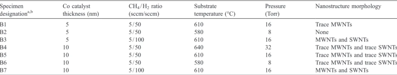
Fig. 1(a) to (e) illustrate the FESEM morphologies of the
nanostructures of Specimens A1 to A5, respectively, under the same process conditions but different buffer layer materials. The wafers inFig. 1(a), 1(b) and 1(d) for Specimens A1, A2 and A4 with no buffer application, ZnS – SiO2 and AlN as
buffer layer materials, respectively, have not CNTs. By contrast, the networks of small sized CNTs can be found in
Fig. 1(c) and 1(e) for Specimens A3 and A5 with Al2O3and
AlON as buffer layers, respectively, where the networks are linked between the neighboring catalyst nanoparticles. This finding indicates that the process is highly promising for 3D circuit manufacture.
To study the nanostructures of the CNTs in Fig. 1(c) and 1(e), the typical HRTEM image of CNTs for Specimens A3 and A5 is shown in Fig. 2, comprising MWNTs (¨10 nm in diameter) and SWNTs (¨1 nm in diameter). Restated, Al2O3
and AlON materials can be the buffer layer candidate materials to encourage the formation of SWNT networks by MPCVD. Notably, the deposition temperature in these cases is around 640 -C, which is much less than that found in the previous works [7 – 11].
To clarify combination effects of thickness of buffer and catalyst layers on nanostructures growth for ZnS – SiO2 and AlN materials, the analytical results show that no CNTs can be identified by raising the thickness of the buffer, catalyst or both layers; except for the AlN buffer layer, MWNTs can be synthesized by raising the thickness of both the buffer and catalyst layers (Specimen A7). This conclusion is conformed to Raman spectroscopy to identify the types of CNTs, as discussed in next paragraph. In conclusion, AlN is not a good candidate buffer layer material for promoting SWNTs synthesis.
The effects of CH4/ H2 ratio, catalyst thickness and
process temperature on FESEM morphologies of the depos-ited nanostructures were then examined on the same AlON buffer material with 10 nm thickness. According to Fig. 1(e), the obvious CNT networks can be found between the Co catalyst particles under 640 -C substrate temperature. However, under the same catalyst thickness of 5 nm, and when the substrate temperature was reduced from 640 to 610
Table 1
Specimen designations and their process conditions of the nanostructures on Si wafer with various buffer layer materials
Specimen designationa,b Buffer layer material and thickness (nm)c Co catalyst layer thickness (nm)c Nanostructure morphology A1 – 5 None A2 ZnS – SiO2(10 ) 5 None A3 Al2O3(10) 5 MWNTs and SWNTs, A4 AlN (10) 5 None A5 AlON (10) 5 MWNTs and SWNTs A6 AlN (10) 10 None A7 AlN (15) 10 MWNTs a
H-plasma pretreatment conditions : pressure ¨30 Torr; microwave power, 400 W; deposition time, 10 min and H2flow rate, 100 sccm.
b
Other deposition conditions of carbon nanostructures: pressure ¨32 Torr; microwave power, 800 W; deposition time, 6 min and CH4/ H2gas ratio, 5
sccm / 50 sccm.
c
Deposition conditions of different buffer layer materials and Co catalyst layer : For ZnS-SiO2(Ar flow, 12 sccm; power, 3 kw). For Al2O3(Ar / O2flow,
15 sccm / 10 sccm; power, 1 kw). For AlN (Ar / N2flow, 15 sccm / 10 sccm;
power, 1 kw). For AlON (Ar / O2/ N2flow, 15 sccm / 2 sccm / 8 sccm; power, 1
kw). For Co (Ar flow, 15 sccm; power, 0.4 kw).
Table 2
Specimen designations and their process conditions of the nanostructures on silicon wafer with AlON (10 nm) as buffer layer Specimen designationa,b Co catalyst thickness (nm) CH4/ H2ratio (sccm/sccm) Substrate temperature (-C) Pressure (Torr) Nanostructure morphology B1 5 5 / 50 610 16 Trace MWNTs B2 5 5 / 50 580 8 None B3 5 5 / 100 610 16 MWNTs and SWNTs
B4 10 5 / 50 640 32 Trace MWNTs and trace SWNTs
B5 10 5 / 50 610 16 Trace MWNTs and trace SWNTs
B6 10 5 / 50 580 8 Trace MWNTs and trace SWNTs
B7 10 5 / 100 610 16 MWNTs and SWNTs
aH-plasma pretreatment conditions : pressure ¨30 Torr; microwave power, 400 W; deposition time, 10 min and H
2flow rate, 100 sccm. b Other deposition conditions of carbon nanostructures: microwave power, 800 W; deposition time, 6 min and CH
or 580 -C (Specimens A5, B1 and B2) changing the system pressure, no detectable CNTs networks were found for temperatures below 610 -C. By contrast, at the same 610 -C substrate temperature, CNTs networks appeared again when the CH4/ H2 ratio was reduced from 5 / 50 to 5 / 100
sccm/sccm (Specimen B3). In summary, the preferred
conditions to form CNT networks between the Co catalyst nanoparticles are high substrate temperatures and low CH4/
H2 ratios.
To examine how catalyst thickness affects the deposited nanostructures, the same experimental conditions in the above paragraph were performed again, except that the catalyst thickness was increased from 5 to 10 nm (Specimens B4 to B7). Experimental results indicate that a substrate temperature of 640-C is insufficiently high to form networks of CNTs under a high CH4/ H2 ratio. By contrast, CNT
networks can be formed for substrate temperatures as low as 610 -C under a lower CH4/ H2 ratio (Specimen B7). These
findings suggest that the most favorable conditions for synthesizing networks of CNTs are a low CH4/ H ratio, high
substrate temperature and low catalyst thickness. Conversely, the findings agree with our previous results that the CH4/ H
ratio is the most important process parameter for varying the deposited structures among diamond film, diamond-like carbon, Si – C – N microcrystals, Si – C – N nanotubes and
CNTs [12,13].
Fig. 1. SEM micrographs of the deposited carbon nanostructures on silicon wafers with various materials as buffer layers of Co catalyst: (a) no buffer layer, (b) ZnS – SiO2, (c) Al2O3, (d) AlN and (e) AlON, respectively (Specimens A1 to A5).
Fig. 2. Typical HRTEM micrographs of the synthesized CNTs using AlON buffer layer material.
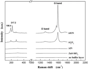
3.2. Raman spectra of the nanostructures
To explore the types of CNTs or nanostructures, Fig. 3 shows the Raman spectra of the nanostructures with no buffer layer and with four different buffer layer materials (Speci-mens A1 to A5). The Raman spectra for Speci(Speci-mens A1, A2 and A4 contained no obvious G-band and D-band peaks with no buffer layers, ZnS – SiO2 and AlN buffer layer materials.
Conversely, a strong peak of radial breath mode (RBM) and a high IG/ ID ratio were obtained for Specimens A3 and A5
with Al2O3and AlON as buffer layers, respectively, showing
the existence of highly graphitized MWNTs and SWNTs. This finding is based on the proposition that the peak intensity of RBM is linked to the quantity of SWNTs in the nanos-tructures [14]. Moreover, the RBM peak is stronger in nanostructures with a buffer layer of AlON than those with Al2O3, indicating that AlON promotes SWNT formation more
effectively than Al2O3. This finding agrees with that of
FESEM examination.
Under the same 10 nm thickness AlON buffer material and the same 5 nm catalyst thickness, the Raman spectra of the nanostructures are shown in Fig. 4 under various substrate temperatures and CH4/ H2 ratios (Specimens B1
to B3), showing that no significant Raman peaks can be identified by reducing the substrate temperatures from 640 to 610 or 580 -C (Specimens A5, B1 and B2). By contrast, a strong RBM peak and high IG/ ID ratio can be observed by
reducing the CH4/ H2 ratio from 5 / 50 to 5 / 100 sccm/sccm
under the same 610 -C substrate temperature (Specimens B3). In other words, a high substrate temperature and a low CH4/ H2 ratio are the two favorable conditions for forming
SWNTs.
Fig. 5shows the Raman spectra of deposited nanostructures
under the same experimental conditions as above, except that the catalyst thickness was increased from 5 nm to 10 nm (Specimens B4 to B7). The results imply that a substrate temperature of 640-C is not high enough to form SWNTs. The results also indicate that a CH4/ H2ratio of 5 / 100 sccm/sccm is
sufficiently low to form SWNTs with strong RBM peaks and high IG/ IDratio even at 610-C (Specimens B7). In summary,
the favorable conditions for forming SWNTs are a high substrate temperature, low CH4/ H2 ratio and low catalyst
thickness.
Tables 1 and 2 also summarize the relationships between
morphologies of the nanostructures and processing conditions. In terms of buffer layer material, these findings suggest that the better materials to increase formation of SWNTs are AlON followed by Al2O3, both of which are Al-based materials. The
other two materials (AlN, ZnS – SiO2) are poor in these
applications, although AlN can be employed to promote formation of MWNTs, but not SWNTs.
Fig. 3. Raman spectra of the deposited carbon nanostructures on silicon wafers with various materials as buffer layers and with no buffer layer.
Fig. 4. Raman spectra of the deposited carbon nanostructures on silicon wafers under the same AlON buffer and catalyst thickness of 5 nm. (a) CH4/ H2ratio,
5 / 50 sccm/sccm; substrate temperature, ¨610-C (Specimens B1); (b) CH4/ H2
ratio, 5 / 50 sccm/sccm; substrate temperature, ¨580-C (Specimens B2), and (c) CH4/ H2ratio, 5 / 100 sccm/sccm; substrate temperature, ¨610-C
(Speci-mens B3).
Fig. 5. Raman spectra of the deposited carbon nanostructures on silicon wafer under the same AlON buffer and catalyst thickness 10 nm of: (a) CH4/ H2ratio,
5 / 50 sccm/sccm; substrate temperature, ¨640-C (Specimens B4); (b) CH4/ H2
ratio, 5 / 50 sccm/sccm; substrate temperature, ¨610-C (Specimens B5). (c) CH4/ H2ratio, 5 / 50 sccm/sccm; substrate temperature, ¨580-C (Specimens
B6), and (d) CH4/ H2ratio, 5 / 100 sccm/sccm; substrate temperature, ¨610-C
3.3. Growth mechanism of CNTs networks
Significantly, CNTs networks closely resemble root-growth CNTs from a catalyst particle, which is much larger than the tubes in size [15]. Fig. 6, with a magnified inset, shows the HRTEM image of the typical CNTs under AlON buffer layer and substrate temperature of ¨640 -C (Specimen A5). The inset demonstrates that nanotubes grow from the small extrusion of a large catalyst. This finding is similar to the proposed mechanisms of the catalyst-split and root-growth models[15,16], where the split catalysts are frequently found at the locations of changing the growth direction. The favored conditions for forming SWNTs are small split catalysts and low growth rates. A high substrate temperature can increase the mobility for splitting and a low CH4/ H2ratio generally results
in a low growth rate due to a small carbon concentration. Furthermore, a thin catalyst thickness produces small nano-particles following H-plasma pretreatment. Concerning the buffer layer material, which may cause the catalysts to deposit to form more nano-extrusions, may favor to form SWNTs from these extrusions. Therefore, the most favorable buffer layer material is AlON, because of its strong tendency to become nano-sized pores on the surface. Further study on this subject is necessary.
4. Conclusions
The growth mechanism and the favorable conditions for fabricating the networks of SWNTs on Si wafers were successfully identified in a MPCVD system with CH4 and
H2 as source gases. The lowest temperature in the present
conditions to form SWNTs is ¨610-C. Experimental results demonstrate that the materials which most effectively promote SWNTs formation are AlON followed by Al2O3. Our results
further demonstrate that AlN buffer material is good only for MWNT fabrication, while ZnS – SiO2 is not a candidate buffer material for CNTs growth. Moreover, the results also indicate that the favorable conditions for synthesizing SWNTs networks are a high substrate temperature, low CH4/ H2ratio and thin
catalyst thickness with AlON as the buffer layer material. In summary, the favorable conditions for forming networks of SWNTs are the conditions for forcing catalyst surfaces to form nano-sized extrusions.
Acknowledgments
This work was supported partly by the National Science Council of Taiwan, under Contract Nos. NSC93-2216-E-009-004, NSC93-2216-E-009-009, and No. NSC93-2120-M-009-003.
References
[1] P.G. Collins, M.S. Arnold, P. Avouris, Science 292 (2001) 706. [2] A. Bachtold, P. Hadley, T. Nakanishi, C. Dekker, Science 294 (2001)
1317.
[3] X. Liu, C. Lee, C. Zhou, J. Han, Appl. Phys. Lett 79 (2001) 3329. [4] M.M.J. Treacy, T.W. Ebbesen, J.M. Gbson, Nature 381 (1996) 678. [5] R. Saito, M. Fujita, G. Dresselhaus, M.S. Dresselhaus, Appl. Phys. Lett.
60 (1992) 2204.
[6] P. Kim, L. Shi, A. Majumdar, P.L. McEuen, Phys. Rev. Lett. 87 (2001) 215502.
[7] T. de los Arcos, M.G. Garnier, P. Oelhafen, D. Mathys, J.W. Seo, C. Domingo, J.V. Garcia-Ramos, S. Sanchez-Cortes, H.J. Dai, J.H. Halfner, A.G. Rinzler, D.T. Colbert, Carbon 42 (2004) 187.
[8] J.M. Ting, C.C. Chang, Appl. Phys. Lett 80 (2002) 324.
[9] L. Delzeit, B. Chen, A. Cassell, R. Stevens, C. Nguyen, M. Meyyappan, Chem. Phys. Lett. 348 (2001) 368.
[10] L. Delzeit, I. McAninch, B.A. Cruden, D. Hash, B. Chen, J. Han, M. Meyyappan, J. Appl. Phys. 91 (2003) 623.
[11] A.M. Cassell, G.C. McCool, H.T. Ng, J.E. Koehne, B. Chen, J. Li, J. Han, M. Meyyappan, Appl. Phys. Lett. 82 (2003) 817.
[12] H.L. Chang, C.H. Lin, C.T. Kuo, Diamond Relat. Mater. 11 (2002) 793. [13] W.H. Wang, Y.T. Lin, C.T. Kuo, Diamond Relat. Mater. 14 (2005) 907. [14] A.M. Rao, E. Richter, S. Bandow, Science 275 (1997) 187.
[15] Y. Saito, M. Qkuda, N. Fujimoto, T. Yoshikawa, M. Tomita, T. Hayashi, Jpn. J. Appl. Phys. 33 (1994) 526.
[16] C.H. Lin, H.L. Chang, C.T. Kuo, Diamond Relat. Mater. 11 (2002) 922. Fig. 6. HRTEM image of the typical CNTs with a magnified inset with AlON