Journal of The Electrochemical Society, 147 (11) 4305-4306 (2000) 4305 S0013-4651(00)03-073-1 CCC: $7.00 © The Electrochemical Society, Inc.
Copper (Cu) contamination1-8in Si complementary metal-oxide-semiconductor (CMOS) based devices has attracted much attention recently, because Cu may come from either the front-end or back-end process. It has been reported that Cu can affect the threshold voltage of MOS transistors,1and form precipitate or silicide at the Si/SiO2interface.5,8The oxide breakdown voltage is reduced under a condition of high contamination levels,2,5,8but, for slight contam-ination, significant electrical degradation only occurs at the field overlap edge3with little effect on the area gate oxide breakdown.4,6,7 While most previous works have primarily focused on the front-end preoxidation Cu contamination, Cu contamination introduced by Cu interconnection processes, such as Cu electroplating and chemical mechanical polishing (CMP) becomes an important concern. In this article, we have examined the gate oxide integrity9,10of Cu-contam-inated MOS capacitors, which received thermal treatment at 4008C after contamination. While the breakdown field and interface trap density deteriorate after Cu contamination, the degradation is insen-sitive to the Cu concentration of the contamination solution in the study. On the other hand, the strong dependence of the pretunneling leakage current on the contamination concentration is observed. The pretunneling current increases monotonically with the amount of Cu contamination and is very similar to stress-induced leakage current (SILC).11-13 Electrical measurements suggest that the possible mechanism of the pretunneling current leakage is attributed to the generation of neutral traps by Cu contamination.
Experimental
Four-inch, p-type Si(100) wafers with a resistivity of 10 V-cm were used in this study. The wafers were cleaned in a 3:1 solution of H2SO4and H2O2, a high purity deionized water rinse, an RCA clean, a 1% HF etch, and a final deionized water rinse. After the growth and patterning of the 3000 Å field oxide, gate oxides of 50 Å in thick-ness were grown by dry oxygen at 9008C. A 3000 Å thick poly-Si was deposited on the gate oxide with subsequent n-type doping using phosphorus. The standard aluminum contact was formed by sputtering, and MOS capacitors of 100 3 100 mm were fabricated. Therefore, the fabricated device structure is 5000 Å Al/3000 Å poly-Si/50 Å gate oxide/Si substrate. Cu was introduced by immersing devices into a CuSO4solution for 60 s. Cu concentration of 10 ppb and 10 ppm were used in this study. The contaminated MOS capac-itor was further annealed at 4008C for 0.5 h (10 ppb contamination) or 1 h (10 ppm contamination) in a nitrogen gas ambient.
Results and Discussion
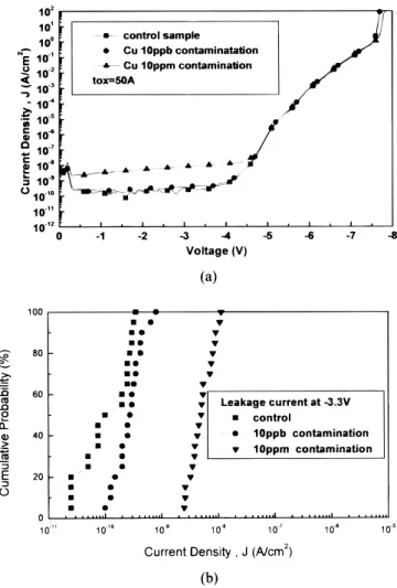
Figures 1a and b show the current density-voltage (J-V) charac-teristics and the accumulative distribution, respectively. Although no effect of Cu contamination concentration on the Fowler-Nordheim (F-N) tunneling current can be found, strong pretunneling current dependence on the Cu contamination is observed. The phenomena of
increasing the pretunneling current without changing the F-N tun-neling current is very similar to SILC effect of gate oxides. The leak-age current in the pretunneling region is attributed to trap-assisted tunneling that saturates or becomes incomparable to F-N tunneling at higher gate bias. Furthermore, a monotonic increase of the pre-tunneling current with increasing the Cu concentration was meas-ured. This effect is similar to SILC, in which a higher leakage
cur-The Effect of Copper on Gate Oxide Integrity
Y. H. Lin,
aY. H. Wu,
aA. Chin,
a,zand F. M. Pan
b aDepartment of Electronics Engineering, National Chiao Tung University, Hsinchu, Taiwan bNational Nano-Device Laboratory, Hsinchu, TaiwanWe have studied the effect of copper contamination after the front-end metal-oxide-semiconductor capacitor fabrication on gate oxide integrity. The significant effect of Cu contamination on the pretunneling current, in combination with insensitive dependence of the Fowler-Nordheim tunneling current, oxide charge density, and breakdown field on the Cu concentration, suggests that the current leakage mechanism may be due to neutral traps generated by Cu inside oxide. In addition to pretunneling oxide leakage, a small amount of Cu contamination increases the interface trap density that may degrade the device performance.
© 2000 The Electrochemical Society. S0013-4651(00)03-073-1. All rights reserved. Manuscript submitted March 4, 2000; revised manuscript received July 22, 2000.
z E-mail: [email protected]
Figure 1. (a) The leakage current density for various copper contamination.
(b) Current density distribution for various copper contamination at 23.3 V bias. The contamination is performed by contacting the devices with 10 ppb or 10 ppm CuSO4solution for 60 s and annealing at 4008C for 0.5 h (10 ppb
contamination) or 1 h (10 ppm contamination) in N2ambient.
) unless CC License in place (see abstract). ecsdl.org/site/terms_use
address. Redistribution subject to ECS terms of use (see 140.113.38.11
4306 Journal of The Electrochemical Society, 147 (11) 4305-4306 (2000)
S0013-4651(00)03-073-1 CCC: $7.00 © The Electrochemical Society, Inc.
rent may be induced with a higher oxide trap generation under a stronger or longer stress condition.11-13
To further examine the effect of Cu contamination on gate oxide integrity, we have measured the breakdown field of the gate oxide as a function of the Cu concentration of the contaminant solution. As shown in Fig. 2, Cu contamination has no obvious effect on the oxide breakdown field. This may be due to a small amount of Cu generating traps inside the oxide and is similar to preoxidation Cu contamination reported previously.4,6,7It is important to note that the weak dependence of the breakdown field on the Cu concentration, in combination with a strong relationship between the measured pre-tunneling current and the Cu concentration, is also consistent with SILC, where no hard breakdown field degradation occurs.9-13
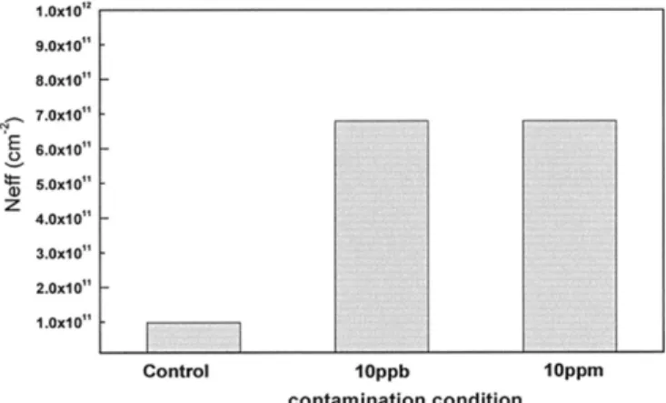
The interface trap density derived from the C-V measurement is shown in Fig. 3. A low interface trap density of 3 3 1010eV21/cm2 is measured for the control sample that is typical for thermal oxides. After Cu contamination, the interface trap density increases. This is attributed to the presence of Cu precipitation at the interface between the Si substrate and the gate oxide.5According to Fig. 3, the inter-face trap density seems not to have an obvious dependence on the Cu concentration. Since the interface trap density is strongly related to the low frequency transistor noise, the increased interface trap den-sity can degrade the device performance to an unacceptable state for ultralarge scale integrated (ULSI) applications.
The oxide charge density as a function of the Cu contamination is shown in Fig. 4. Although the oxide charge density is higher for the contaminated device than for the control sample, there is no noticeable dependence of oxide charge density on the Cu
concentra-tion. Therefore, the higher leakage current observed in Fig. 1 is not due to the oxide charge. It is reported that SILC may be due to neu-tral traps formed by hole injection into the oxide.12,13The negligible dependence of the oxide charge density on the Cu concentration also suggests that neutral traps formed by Cu inside the oxide matrix may be responsible for the higher pretunneling leakage current. The rea-son why such effect is not observed in the preoxidation contamina-tion may be due to different mechanisms. Cu can be oxidized to form Cu oxide and join the SiO2matrix in preoxidation contamination, while in the present paper elemental Cu or the Cu ion is present inside the SiO2matrix instead of the Cu oxide form.
Conclusions
We have studied the effect of Cu contamination on gate oxide integrity after front-end MOS capacitor fabrication. The strong de-pendence of pretunneling current on the Cu concentration, in combi-nation with insensitive F-N tunneling current, oxide charge density, and breakdown field to the Cu contamination level, suggests that the mechanism may be due to neutral traps generated by Cu inside the oxide.
Acknowledgments
Support by the National Science Council of the R.O.C. under contract no. 89-2215-E-317-006 and NSC89-2721-2317-200 is gratefully acknowledged.
National Chiao Tung University assisted in meeting the publication costs of this article.
Reference
1. B. Vermeire, C. A. Peterson, H. G. Parks, and D. Sarid, in Proceedings of Interna-tional Reliability Physics Symposium, p. 315 (1999).
2. D. A. Ramappa and W. B. Henley, J. Electrochem. Soc., 146, 2258 (1999). 3. B. Vermeire, L. Lee, and H. G. Parks, IEEE Trans. Semicond. Manuf., 11, 232
(1998).
4. T. Gravier, F. Braud, J. Torres, J. Palleau, A. Chantre, and J. Kirtsch, Microelectron. Eng., 33, 211 (1997).
5. A. Correia, D. Ballutaud, and J. L. Naurice, Jpn. J. Appl. Phys., 33, 1217 (1994). 6. H. G. Parks, R. D. Schrimpf, B. Craigin, R. Jones, and P. Resnick, IEEE Trans.
Semicond. Manuf., 7, 249 (1994).
7. S. Verhaverbeke, M. Meuris, P. W. Mertens, and M. M. Heyns, Tech. Dig. Int. Elec-tron Devices Mtg., p. 71 (1991).
8. H. Wendt, H. Cerva, V. Lehmann, and W. Pamler, J. Appl. Phys., 65, 2402 (1989). 9. A. Chin, B. C. Lin, W. J. Chen, Y. B. Lin, and C. Tsai, IEEE Electron Device Lett.,
EDL-19, 426 (1998).
10. A. Chin, C. C. Liao, C. H. Lu, W. J. Chen, and C. Tsai, in Proceedings of the Sym-posium on VLSI Tech., p. 135 (1999).
11. B. C. Lin, Y. C. Cheng, A. Chin, T. Wang, and C. Tsai, in Proceedings of Interna-tional Solid State Devices and Materials Conference, p. 110 (1998).
12. K. Sakakibara, N. Ajika, M. Hatanaka, and H. Miyoshi, in Proceedings of the Inter-national Reliability Physics Symposium, p. 100 (1996).
13. G. J. Hemink, K. Shimizu, S. Aritome, and R. Shirota, in Proceedings of the Inter-national Reliability Physics Symposium, p. 117 (1996).
Figure 2. Gate oxide breakdown electric field distribution.
Figure 3. Interface trap density for various copper contamination.
Figure 4. Oxide charges comparison among different contaminated conditions.
) unless CC License in place (see abstract). ecsdl.org/site/terms_use
address. Redistribution subject to ECS terms of use (see 140.113.38.11