Abstract—This paper presents and analyzes a fully digital instruction-cycle-based dynamic voltage scaling (iDVS) power management strategy for low-power processor designs. The pro-posed iDVS technique is fully compatible with conventional DVS scheduler algorithms. An additional computer aided design-based design flow was embedded in a standard cell library to implement the iDVS-based processor in highly integrated system-on-a-chip applications. The lattice asynchronous self-timed control digital low-dropout regulator with swift response and low quiescent cur-rent was also utilized to improve iDVS voltage transition response. Results show that the iDVS-based processor with the proposed adaptive instruction cycle control scheme can efficiently perform millions of instructions per second during iDVS transition. The iDVS-based digital signal processor chip was implemented in a HH-NEC 0.18-µm standard complementary metal-oxide semicon-ductor. Measurement results show that the voltage tracking speed with 11.6 V/µs saved 53% power.
Index Terms—Buck converter, digital signal processor (DSP), dynamic voltage scaling (DVS), fast transient, low dropout (LDO) regulator, low-power design, million instructions per second (MIPS) performance, SoC, switching regulator.
I. INTRODUCTION
P
ERSONAL portable electronics are essential products in our daily lives and are being used for entertainment, for communication, and as biomedical measurement devices. Portable electronics contain processors, such as digital signal processors (DSPs), advanced reduced instruction set computing machines (ARM), and microcontroller units (MCU), as core components. Therefore, designing a low-power processor to extend the battery life of portable devices and to save more power is a critical design target.Manuscript received January 30, 2013; revised March 26, 2013; accepted July 05, 2013. Date of publication August 15, 2013; date of current version October 19, 2013. This paper was approved by Guest Editors Hong June Park and Chang-Hyun Kim. This work was supported by the National Science Council, Taiwan, under Grant NSC 101-2220-E-009-047, Grant NSC 101-2220-E-009-052, and Grant NSC 101-2622-E-009-004-CC2.
S.-Y. Peng, T.-C. Huang, Y.-H. Lee, C.-C. Chiu and K.-H. Chen are with the Institute of Electrical Control Engineering, National Chiao Tung University, Hsinchu 30010, Taiwan (e-mail: [email protected]; [email protected]).
Y.-H. Lin, C.-C. Lee, T.-Y. Tsai and C.-C. Huang are with Realtek Semicon-ductor Corporation, Hsinchu 30076, Taiwan.
L.-D. Chen and C.-C. Yang are with the Industrial Technology Research In-stitute, Hsinchu 31040, Taiwan.
Digital Object Identifier 10.1109/JSSC.2013.2274885
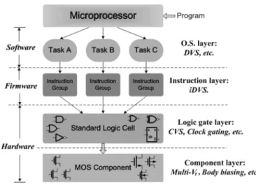
Fig. 1. Low-power management strategy for processors.
Fig. 1 shows the hierarchical processor architecture and demonstrates that programs are executed from the high-level operating system (OS) layer to the lowest component layer. The program, which is stored in the memory, is accessed by the OS for dispatching and scheduling of many different priority tasks, in which the basic unit of a task is the indi-vidual instruction. After the processor decodes the instructions, logic gate circuits are activated to perform specific compu-tations. The corresponding layer then accepts these logical control signals to enable or disable millions of complementary metal–oxide–semiconductor (CMOS) transistors. Hence, var-ious techniques have been presented based on the hierarchical processor architecture to reduce the power consumption of processors.
In Fig. 1, down to the lowest level, which is the CMOS process component layer, multiple-threshold voltage and body bias adjustment techniques are employed in [1]. For simplicity, the clustered-voltage-scaling (CVS) technique at the logic gate layer is adopted in [2]. These techniques have limited power reduction capabilities and require foundry process support or careful layout placement of logical-cell with multipower grids. By contrast, the dynamic voltage scaling (DVS) technique in the OS layer is an effective technique in reducing power consumption because the dynamic power consumption depends
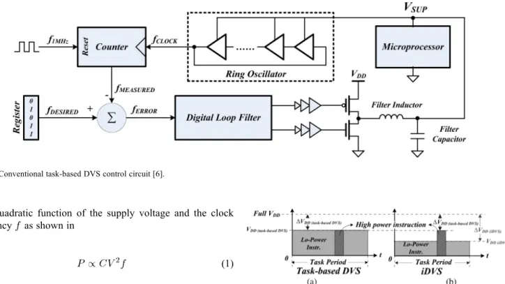
Fig. 2. Conventional task-based DVS control circuit [6].
on a quadratic function of the supply voltage and the clock frequency as shown in
(1) where is the equivalent dynamic operation capacitance.
DVS technique is appropriate for low-power DSP designs fabricated by using standard CMOS processes [3]–[5]. The conventional DVS task-based control circuit [6] as depicted in Fig. 2 uses a closed loop to ensure that the clock fre-quency meets the desired processor operating clock frefre-quency , which is assigned by the OS to the frequency register for a specific task execution. If the peak performance is not necessary, the processor operation clock frequency can be degraded for power saving. Here, the ring oscillator converts the real-time supply voltage , which is generated by an inductor-based switching regulator (SWR), into digital nu-merical clock frequency . The is compared with the to determine the digital frequency error signal and to produce the control signal through the digital filter. Finally, the drivers after the digital loop filter turn on/off the power MOSFETs to modify the output voltage . Therefore, the processor clock frequency is rapidly changed to achieve the dynamic frequency scaling (DFS) according to the minimum and dynamically generated supply voltage. Because the power supply regulator is an inductor-based converter, the DVS tracking speed is restricted from a few microseconds to a few milliseconds. Thus, various fast voltage tracking methods for high-performance DVS response have been reported [7], [8].
The conventional task-based DVS technique allows all tasks in a scheduler to complete just-in-time operations. Thus, the OS depends on run-time workload and dynamically adjusts the supply voltage, thereby leading to substantial power sav-ings [9], [10]. However, the conventional task-based DVS is limited to the highest power instruction of a task operation, as illustrated in Fig. 3(a). Fig. 3(b) shows that conventional task-based DVS with conservative scheduler will fail to operate if the processor has no slack time. Therefore, conventional task-based DVS techniques are designed to change the pro-cessor operating clock frequency to facilitate the voltage scaling
Fig. 3. (a) Conventional task-based DVS is limited by the high power instruc-tion. (b) iDVS effectively reducing power consumpinstruc-tion.
operation. However, these techniques induce several problems when controlling peripheral modules, that is, rapidly changing processor clock frequency will result in control signal timing errors and missing of communication data latch in peripheral devices, such as synchronous dynamic random access memory (SDRAM), inter-integrated circuit , analog-to-digital converter (ADC), digital-to-analog converter (DAC), universal asynchronous receiver/transmitter (UART), and flash memory peripheral interface. The reason for this drawback is the de-pendence of peripheral devices in system on chip (SoC) on constant clock and predictable control signals.
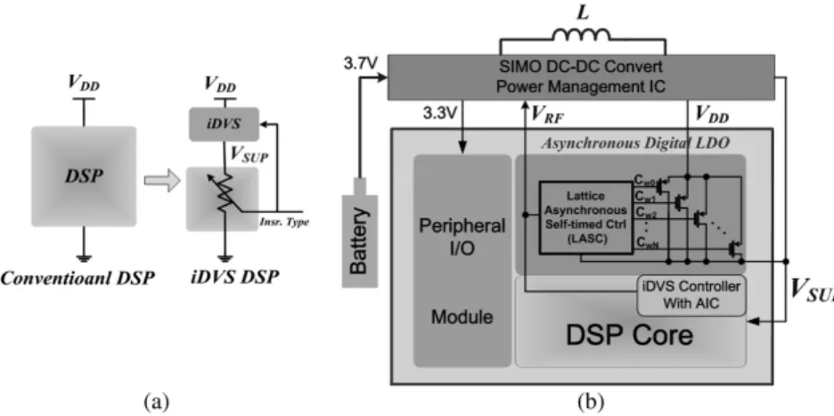
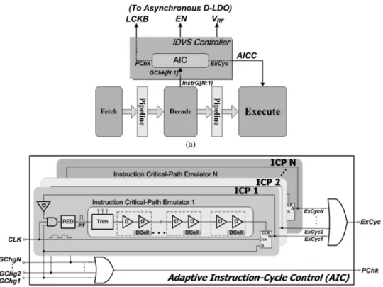
To overcome the aforementioned design challenges, this paper proposes an instruction-cycle-based dynamic voltage scaling (iDVS) technique and employs this technique in the instruction layer [11]. Even in the absence of slack time, as shown in Fig. 3(b), the iDVS can effectively reduce power consumption better than the conventional task-based DVS technique can. As depicted in Fig. 4(a), the processor works as a dynamic loading and is emulated by an adjustable resistor, which is controlled by the instructions. In this paper, the iDVS power management, which is based on different instructions, does not require changing or stalling of the processor op-erating clock frequency. Instead, the iDVS ensures that the processor performs with minimum power supply. Through the task-based DVS, energy can be reduced when tasks have low power consumption. Therefore, iDVS is more appropriate for low-power DSP designs. Fig. 4(b) shows a DSP employing the proposed iDVS topology. The core component of the iDVS includes a lattice asynchronous self-timed control (LASC) digital low-dropout (D-LDO) regulator and an iDVS controller with an adaptive instruction-cycle control (AIC) circuit. The
Fig. 4. (a) Concept of the iDVS operation. (b) iDVS processor block diagram.
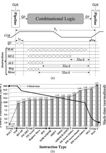
Fig. 5. Stages and critical paths during instruction execution.
D-LDO regulator and the AIC circuit guarantee fast voltage tracking speed and high operation frequency.
The remaining parts of this paper are organized as follows. Section II describes the proposed iDVS mechanism. Section III presents a design flow for the iDVS-based processor with automatic computer-aided design (CAD) tools. Section IV illustrates the adaptive instruction-cycle control. Section V presents the fast transient and low-power LASC D-LDO reg-ulator. Section VI presents the experimental results. Finally, Section VII concludes the paper.
II. PROPOSEDiDVS MECHANISM
Processors are designed to operate with versatile appli-cation programs. When taking a phone call, the OS of an embedded system issues the key-scan service and speech com-pressing/decompressing code-excited linear prediction (CELP) algorithm once mobile phone buttons are pushed. Similarly, when listening to a moving picture experts group audio layer III (MP3) and simultaneously browsing a picture from the flash memory device, the OS dispatches the file-system access and the MP3/joint photographic experts group (JPEG) decoding
algorithm. Although these task programs have different charac-teristics, their fundamental unit is still the instruction unit. The basic steps of program execution in a processor are instruction fetching, decoding, executing, and storing, as illustrated in Fig. 5(a). The most complicated part is the execution unit in Fig. 5(b), which can provide all types of hardware circuits to support different complex instructions. Each instruction has its corresponding critical data path to complete execution. Critical paths occupy only a small fraction of the total number of paths within a chip. Unfortunately, the clock speed of a synchronous processor is determined by the worst delay of the critical paths. These critical paths usually map high-power-consuming and long data path instructions that are subjected to single-instruc-tion multiple-data (SIMD) instrucsingle-instruc-tions, such as divide (DIV), normalize (NORM), and multiply-and-accumulate (MAC). Long slack time exists in noncritical path instructions. Fig. 6(a) shows the slack time in different instructions. Fig. 6(b) shows the measured slack time and power consumption of various instructions at the supply voltage fixed at 1.8 V. Consequently, a longer slack time corresponds to a smaller supply voltage that can be provided by the proposed iDVS. However, reducing the
Fig. 6. (a) Slack time in different instructions. (b) Measured slack time and power consumption of different instructions.
supply voltage affects the propagation delay in the CMOS circuit. As shown in
(2) where is inversely proportional to the supply voltage , where and are foundry process parameters [12].
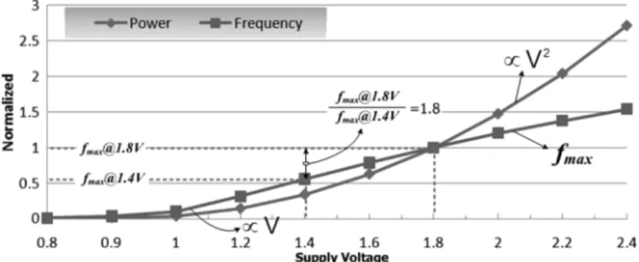
The test chip of a 23-stage ring oscillator in a 0.18- m CMOS process uses 1.8-V core devices. Fig. 7 shows the maximum operating frequency and total power consumption with re-spect to supply voltage variation. According to the results of the supply voltage with 1.8 V, the unit of the y-axis is the normal-ized operating frequency and the normalnormal-ized power consump-tion. The result reveals that the relationship between the circuit operation frequency and the supply voltage is linear from 1.2 to 1.8 V. Moreover, if the is scaled down from 1.8 to 1.4 V, the is still larger than half of the maximum oper-ating frequency at 1.8 V. Thus, the scaling range of the for the normal operation in the proposed iDVS ranges from 1.2 to 1.8 V, excluding the HALT and no operation (NOP) instruc-tions. The minimum should be larger than 1 V; otherwise, the level-shift signal will experience serious delay when travel-ling from the level-shift circuit to peripheral I/O modules.
Power reduction is obvious if the proposed iDVS mechanism lowers the supply voltage of the instruction execution on the
non-critical path while maintaining a higher supply voltage on the critical paths to satisfy complex instruction timing requests. Therefore, the DVS dynamically adjusts the supply voltage on the basis of the instruction-cycle domain to guarantee that suf-ficient power is provided for correct execution of instructions. In addition, iDVS requires the regulator to have high-speed voltage tracking capability to provide in-demand power for instruction execution. Thus, the DSP chip has an embedded all-digital LASC D-LDO regulator with low quiescent current to meet the required voltage tracking speed. Consequently, processor performance degrades when iDVS operates during voltage transition. In previous systems, voltage transition will stall the entire processor operation unless the required power for the instruction is available, which results in the serous degradation of the million instructions per second (MIPS) performance.
To avoid the aforementioned drawbacks, the proposed LASC D-LDO regulator obtains help from the adaptive instruc-tion-cycle control (AIC) circuit. The LASC D-LDO regulator with ultra-low quiescent current at light loads can offer rapid voltage tracking speed during voltage transition. The AIC scheme can adaptively adjust the instruction execution cycle time to guarantee that each instruction is correctly executed during voltage tracking for high-performance iDVS operation, that is, the iDVS-based design processor does not change the processor clock frequency or stall the entire processor clock during DVS operation. As a result, the processor performance is maintained without adjusting the clock frequency to be more suitable for control of peripheral I/O devices in the SoC.
III. DESIGNFLOW FOR THEiDVS-BASEDPROCESSOR
WITH THEAUTOMATICCAD TOOLS
Identifying the corresponding critical data path for each in-struction and relative operating voltage for the iDVS technique is an important issue because thousands of data paths and mil-lions of logic gates are deployed in a processor. Analyzing the correlation between critical data paths and instructions manu-ally would be impractical. Therefore, CAD tools are utilized to provide an effective route for analyzing this correlation. To create the parameters required by the instruction critical path (ICP) emulator, circuit extraction tools obtain register-transfer level (RTL) components and parasitic resistor/capacitor (RC) on the instruction critical path. The extracted circuit netlist from the target processor can be used for Spice simulation to obtain min-imum operation voltage for each instruction. In the conventional design flow, CAD tools also help analyze and optimize the final chip operation timing/function correctly under process, voltage, and temperature (PVT) variations.
Fig. 8 illustrates the standard cell library design flow in an iDVS-based processor. The design flow contains the three steps outlined below. First, hardware specifications are coded into hardware description language (HDL) according to traditional design flow to synthesize the cell-based circuit for post-simula-tion, which can check the function and verify timing. The crit-ical path of each instruction at the post-stimulation stage can
Fig. 7. Normalized operating frequency and normalized power consumption versus supply voltage in a 23-stage ring oscillator fabricated in 0.18- m CMOS process.
Fig. 8. Standard cell library design flow with the proposed iDVS design flow.
be obtained by using the standard cell library with the RC ex-traction and timing analysis tool in the proposed iDVS-based processor. Spice simulation can be conducted to establish the critical path table for correlating minimum operating voltage to each corresponding instruction. The timing parameter of each instruction critical path is also extracted to create the ICP in the AIC circuit. Final step is backward annotation of each instruc-tion power catalog and timing constraint to the iDVS controller in the HDL design. Owing to the help of the RC extraction and the timing analysis tools, the iDVS technique can fit any stan-dard cell library provided by the foundries.
IV. ADAPTIVEINSTRUCTION-CYCLECONTROL
The instruction unit occupies one clock cycle in the reduced instruction set computing (RISC) design. However, a real-time adaptive instruction cycle should be performed in the AIC cir-cuit of the proposed iDVS to adapt to the scaling supply voltage level of the LASC D-LDO regulator. Fig. 9(a) and (b) show the topologies of the iDVS controller and the AIC circuit, respectively. The ICP in Fig. 9(b) emulates the relative in-struction group critical-path delay, which is synthesized by the standard-cell delay component after timing verification through the proposed iDVS CAD design flow. Instructions that have the same characteristic of data path or power consumption are grouped into one ICP emulator. The current AIC design has four ICP emulators. Each ICP contains a rising edge detector (RED), standard-cell delay components, a delay trimming module, and control logics. The delay trimming module is an option for minimizing mass-production deviation after minor
adjustment. Fig. 10 shows the operation states of the iDVS controller with the timing diagrams as depicted in Fig. 11.
The DSP instruction cycle is synchronous with the edge-trig-gered clock signal . In each cycle, the different instruc-tions shown in Fig. 6 are decoded to generate the instruction group signal . When the DSP consecutively exe-cutes the instruction stream, the iDVS controller monitors the required power for each instruction according to the instruc-tion power table, which is generated by the iDVS CAD design flow. Once the iDVS detects that the required execution-power of the next instruction is different from that of the current ex-ecution instruction group, the instruction group in accordance with the instruction group change the signals is-sued to the AIC circuit. In the next stage, the iDVS controller enters the tracking mode state from the operation state to acti-vate the LASC D-LDO regulator by setting the signal to high. As shown in Fig. 11(a), due to the characteristic of the DSP pipeline structure, the voltage transition command is is-sued before an instruction is executed prior to one clock cycle. Once RED detects the instruction group change signals, which are synchronized with , RED will induce one pulse signal to the ICP emulator. The next operation of the AIC circuit is similar to the race condition to test whether the instruction can complete execution within one instruction cycle under the present supply voltage . If passes through the ICP em-ulator and simultaneously exceeds the rising edge of the , then the AIC circuit will pull low the signal . is synchronized by the iDVS controller to generate the signal
Fig. 9. (a) Topology of the iDVS controller with the AIC circuit. (b) AIC circuit.
Fig. 10. Operation states of the iDVS controller.
to informing the DSP execution unit that an extra cycle is not needed during the instruction cycle.
On the other hand, the passing of through the ICP em-ulator and the lag of the rising edge of the indicates that insufficient power is provided by the . The DSP needs to insert an extra cycle to complete the current instruction exe-cution by setting to high. According to (2) and Fig. 7, there will no instruction required to exceed two cycles for exe-cution in the section 1.4 1.8 V. Owing to the instruction pre-de-coding of the pipeline structure and fast transition response of the LASC D-LDO regulator, the iDVS-based DSP only needs one extra-cycle during the up-tracking voltage transition. If the iDVS controller detects the low level of the within two successive instruction cycles, the supply voltage is well-regu-lated and sufficient for the instruction execution. The iDVS con-troller then withdraws the power check request signal and returns to the locking mode by setting the to low.
Conversely, the supply voltage is sufficiently high to avoid blocking of DSP execution flow during down-tracking voltage transition. The control sequence of the down-tracking voltage transition is as follows. First, the D-LDO regulator pulls low the . The iDVS controller then sends the group change signals to the AIC circuit and continuously monitors the comparison result of the with the reference voltage . Finally, the iDVS controller returns to the locking mode by setting the to low until the and the have two crossover points after the signal is main-tained at low levels within two successive instruction cycles as depicted in Fig. 11(b). Simultaneously, the iDVS controller withdraws the power check request signal . The supply voltage is adequate for instruction execution in the locking mode. Therefore, correct instruction execution can be achieved during iDVS voltage transition without stopping the operation clock by using the proposed AIC mechanism.
V. PROPOSEDLASC D-LDO REGULATOR
Low-power DSP designs are on the cutting-edge of ad-vance processes. Digital processes are more mature than analog processes. Thus, the all-digital LDO has wide oper-ating voltage range from the device threshold voltage, , to the highest supply voltage and requires minimal biasing current to ensure voltage regulation. The all-digital LDO is also more suitable for embedded iDVS-based processor de-signs. All digital clock-based LDO regulators [13], [14] and inductor switching type dc–dc converters [15] demonstrate fast voltage transition response but require high-frequency operation clock, which results in substantial power con-sumption. To meet versatile power demand from processor
Fig. 11. Timing diagram of the iDVS operation. (a) Up-tracking condition. (b) Down-tracking condition.
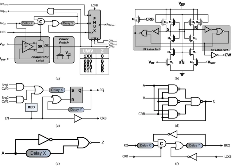
Fig. 12. Implementation of an asynchronous D-LDO regulator with LASC.
instructions, the iDVS-based LDO should have the advan-tage of easily extended driving capability without increasing design complexity. Therefore, this paper proposes the capac-itor-free LASC controlled D-LDO regulator to provide rapid transient supply voltage and low-quiescent-current regulator, as depicted in Fig. 12, because the iDVS technique needs fast voltage tracking. The lattice structure of the LASC
D-LDO regulator is easily extendable and does not require a constant clock to trigger each self-timed control units (SCUs) to provide voltage regulation. The operation of the LASC is similar to a clock-free bidirectional shift register for determining power switch activation. Without utilization of the synchronous clock, the asynchronous control realizes the hand-shaking operation between adjacent SCU stages.
Fig. 13. Implementations of (a) SCU, (b) SR-latch comparator, (c) HR, (d) Muller C-gate, (e) rising edge detector (RED), and (f) TR.
The driven source is an event so that the problems of clock skew and synchronous surge current never occur.
The LASC D-LDO regulator comprises SCU, SR-latch com-parator, heading reflector (HR), and terminal reflector (TR), as shown in Fig. 13. The SCU in Fig. 13(a) contains a Muller C-gate, an SR-latch comparator, a power switch, a path mul-tiplexer, and control logics to modulate power switches to ob-tain the regulated . The SR-latch comparator, as shown in Fig. 13(b), is triggered by the high-level activation of enabling signal , which is controlled by the forward request pulse of the previous stage. The dynamic comparator compares the with the to generate the signal to control the corresponding power switch. The path multiplexer determines the forward request signal from either the prior stage
or from the later stage backward request signal
according to the results, , , and . The table in Fig. 13(a) shows the overall operating principle of the SCU-based Muller C-gate self-timed control. Fig. 13(c) shows that HR ensures that all SCUs in the LASC D-LDO regulator return to their initial states. HR also guarantees that power switches are turned off by setting the signal to low when the signal is forced to low by the iDVS controller. The Muller C-gate in Fig. 13(d) is a basic component of asynchronous circuits. The behavior of an n-input Muller C-gate changes the output state to high if all inputs are high and to low if all inputs are low;
otherwise, the n-input Muller C-gate keeps the output the same as the previous state. As shown in Fig. 13(e), RED generates a single pulse to trigger the HR circuit to pump the first request pulse, thereby activating the LASC D-LDO regulator when the changes from low to high by the iDVS controller. To deal with boundary condition, the TR circuit as depicted in Fig. 13(f), helps the forward request signal reflect form the termination when the cannot acquire sufficient power supply at the final SCU stage. Furthermore, the HR prevents the backward re-quest signal from missing when the derives an overcharge load at the first SCU stage.
Fig. 14(a) and (b) illustrates the timing diagram of the single SCU stage operation at different conditions for corresponding circuit Fig. 13(a). When is smaller than the reference voltage in an SCU stage that is triggered by the signal from the prior stage, the level-active SR-latch comparator out-puts the low-signal to turn on the power switch. Thus, the voltage for the can be increased to track the . The for-ward request signal is generated by self-time control mechanism after a deterministic delay, “ ,” when the next SCU stage performs shift-right operation, thereby activating additional power switches to regulate . If is greater than , then the control signal will be pulled high to turn off the power switch of this stage. The backward request signal will be triggered by the self-time
mech-Fig. 14. Timing diagrams. (a) Single SCU operation when the is smaller than the . (b) Single SCU operation when the is larger than the . (c) LASC operation when is activated.
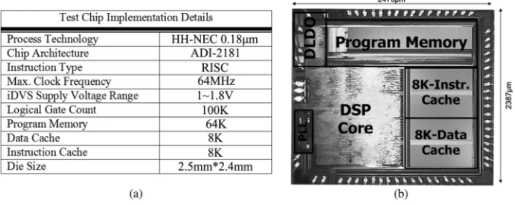
Fig. 15. (a) Chip specifications. (b) Chip micrograph.
anism after a deterministic delay, “ ,” when the prior SCU stage performs shift-left operation to reduce driving capability.
Fig. 14(c) shows the operation timing diagram of the LASC D-DLO regulator. First, is pulled low, and the signal is forced to high by the iDVS controller during the power-on reset state. All SCU stages are initialized to turn off all power switches. Once the processor power-on sequence is completed, the signal is forced to high by the iDVS controller then the HR SCU pumps the first request signal into the LASC controller such that the asynchronous D-LDO regulator output voltage can start tracking the reference voltage according to the instruction demand power. In the up-tracking period, the LASC acts as shift-right operation to turn on more power switches by shifting the control signals from to . When reaches its target value of , the backward request signals are issued to stop the delivery of supplementary power to the . When the LASC operation is converged to the adjacent SCU stages or when the present supply voltage is adequate for normal instruction execution
which is verified by the AIC circuit, the signal is cleared by the iDVS controller to change the operation state from the tracking mode and return the state to the locking mode. The LASC D-DLO regulator operation ends through the indication of the signal . Thus, output voltage ripples are eliminated in the proposed LASC D-LDO regulator because all SCUs are in a steady state. Therefore, all devices are in a static state, the current consumption has closely approached the 0.18- m process, and the core devices leakage current is approximately 80 nA because of the fully digital designed D-LDO regulator. The proposed LASC D-LDO regulator simultaneously achieves fast response and ultra-low static current consumption.
VI. EXPERIMENTALRESULTS
Power management based on the iDVS mechanism equipped with all-digital fast-response LASC D-LDO regulator and the AIC scheme, which is embedded in the DSP, was implemented in 0.18- m CMOS standard process. Fig. 15 shows the spec-ifications and chip micrograph of the proposed mechanism. The measurement results in Fig. 16(a) reveal that the power
Fig. 16. (a) Measured power consumption in different types of instructions with and without iDVS. (b) Measured waveforms of the iDVS operation.
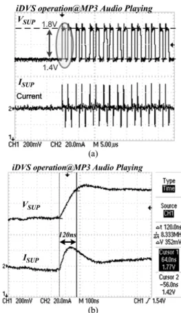
consumption of the general operation instructions was reduced to approximately 50% after iDVS activation. Fig. 16(b) shows the iDVS output voltage with different instructions, and Fig. 17 shows the measured LASC D-LDO regulator with 128-stage output voltage transient waveform when the DSP performs the MP3 audio algorithm of the polyphase filter sec-tion. DSP intensively executes the serial instructions of SIMD and the circular buffer data move. The waveforms exploit the dynamic transient response of the LASC D-LDO regulator supply voltage, making the voltage tracking response time smaller than 120 nS. The LASC D-LDO regulator consumes 200 A during the DVS transient period and 80 nA during the quiescent operation mode. The LASC D-LDO regulator helps the system achieve a current efficiency of 99.96%. Table I compares the characteristics of LASC D-LDO regulator with previous schemes.
The computational load in the DSP chip varies according to task characteristic. However, the basic unit of task is instruc-tion. For example, multiple and convolution MAC instructions rarely appear in the disk service task, but the MP3 audio de-coder requires 34% MAC instructions. This factor affects the iDVS power saving efficiency, as shown in Fig. 18.
The iDVS mechanism will block the DSP performance when heavy load task is executed. In addition, the MP3 and JPEG al-gorithms accounts for 34% of the MAC or high computation in-struction. Therefore, 34% of power miss will occur. However,
Fig. 17. (a) Measured waveforms of the iDVS with fast transient response. (b) Zoom-in waveforms showing fast transient response.
Fig. 18. (a) Measured power reduction contributed by the proposed iDVS tech-nique. (b) Instruction ratio under different application tasks.
an investigation of the 34% DSP instructions reveals that the eration includes signal processing of convolution and matrix op-eration. The MP3 polyphase filter equation and the JPEG image
Fig. 19. Throughput MIPS of the iDVS-based DSP.
discrete-cosines transform equation are shown, respectively, in [18], [19]
(3)
for otherwise
(4) where represents the frame-based 512-point of audio input data, stands for polyphase filter coefficient, is the subband output data, represents the 2D block-based 8 8 matrix of the image input, and stands for the image frequency domain spectrum.
Inherently, the characteristics of these equations contain a large number of frame-by-frame or block-by-block processing signals. Coding these equations into the DSP programs is also presented in grouping and consecutive for the DSP execution. Thus, 34% MAC instruction is not a normal distribution in the instruction stream. When the iDVS performs voltage transition,
only the up-tracking request is required to insert an extra cycle for correct execution. But the DSP programmer or compiler should avoid generating high power miss-ratio coding sequence. There is a trade-off between the MIPS and the power consump-tion. The experimental results reveal that a well-designed DSP program can suppress power miss-ratio from 0.5% to 1.5%. Fig. 19 shows the MIPS performance with power miss-ratio deviation ranging from 10% to 0.5%. The iDVS mechanism demonstrates that the MIPS can be improved by 2.4 and 1.2 times when the power miss-ratio is 10% and 0.5%, respectively, through the activation of the AIC scheme. As a result, the pro-posed iDVS power-management strategy can obtain a peak of 53% power savings. A total of 92% power reduction can also be achieved during sleep mode, thereby extending further the battery life of portable devices.
VII. CONCLUSION
This paper presents an iDVS power management strategy with an all-digital LASC D-LDO regulator. The prototype of the iDVS-based DSP chip is implemented in an HH-NEC 0.18- m standard CMOS process. The DSP chip with the pro-posed iDVS obtains 53% power savings compared with a DSP chip without iDVS. Embedding the LASC D-LDO regulator enables the system to achieve fast-response and low-quiescent current. The MIPS performance can be maintained by the iDVS-based DSP through the utilization of the proposed AIC technique and the LASCD-DLO regulator. Furthermore, the
standard cell library design flow for the iDVS processor and the all-digital LASC LDO regulator are amenable to standard digital CMOS processes. Therefore, the proposed iDVS power management strategy significantly facilitates the iDVS-based low-power DSP design.
REFERENCES
[1] M. Miyazaki, G. Ono, and K. Ishibashi, “A 1.2-GIPS/W processor using speed-adaptive threshold voltage CMOS with forward bias,”
IEEE J. Solid-State Circuits, vol. 37, no. 2, pp. 210–217, Feb. 2002.
[2] K. Usami, M. Igarashi, F. Minami, T. Ishikawa, M. Kanzawa, M. Ichida, and K. Nogami, “Automated low-power technique exploiting multiple supply voltages applied to a media processor,” IEEE J.
Solid-State Circuits, vol. 33, no. 3, pp. 463–472, Mar. 1998.
[3] N. Ickes, G. Gammie, M. E. Sinangil, R. Rithe, J. Gu, A. Wang, H. Mair, S. R. Datla, B. Rong, S. Honnavara-Prasad, L. Ho, G. Baldwin, D. Buss, A. P. Chandrakasan, and U. Ko, “A 28 nm 0.6 V low power DSP for mobile applications,” IEEE J. Solid-State Circuits, vol. 47, no. 1, pp. 35–46, Jan. 2012.
[4] M. Ashouei, J. Hulzink, M. Konijnenburg, J. Zhou, F. Duarte, A. Breeschoten, J. Huisken, J. Stuyt, H. de Groot, F. Barat, J. David, and J. V. Ginderdeuren, “A voltage-scalable biomedical signal processor running ECG using 13 pJ/cycle at 1 MHz and 0.4 V,” in IEEE Int.
Solid-State Circuits Conf. Dig. Tech. Papers, Feb. 2011, pp. 332–334.
[5] S. R. Sridhara, M. DiRenzo, S. Lingam, S.-J. Lee, R. Bl’azquez, J. Maxey, S. Ghanem, Y.-H. Lee, R. Abdallah, P. Singh, and M. Goel, “Microwatt embedded processor platform for medical system-on-chip applications,” IEEE J. Solid-State Circuits, vol. 46, no. 4, pp. 721–730, Apr. 2011.
[6] T. D. Burd, T. A. Pering, A. J. Stratakos, and R. W. Brodersen, “A dy-namically voltage scaled processor system,” IEEE J. Solid-State
Cir-cuits, vol. 35, no. 11, pp. 1571–1580, Nov. 2000.
[7] Y.-H. Lee, C.-C. Chiu, S.-Y. Peng, K.-H. Chen, Y.-H. Lin, C.-C. Lee, C.-C. Huang, and T.-Y. Tsai, “A near-optimum dynamic voltage scaling (DVS) in 65 nm energy-efficient power management with frequency-based control (FBC) for SoC system,” IEEE J. Solid-State
Circuits, vol. 47, no. 11, pp. 2563–2575, Nov. 2012.
[8] Y.-H. Lee, S.-Y. Peng, A. C.-H. Wu, C.-C. Chiu, Y.-Y. Yang, M.-H. Huang, K.-H. Chen, Y.-H. Lin, S.-W. Wang, C.-Y. Yeh, C.-C. Huang, and C.-C. Lee, “A 50 nA quiescent current asynchronous digital-LDO with PLL-modulated fast-DVS power management in 40 nm CMOS for 5.6 times MIPS performance,” in Proc. IEEE Symp. VLSI Circuits, 2012, pp. 178–179.
[9] Y. Liu and M. Lin, “On-line and off-line DVS for fixed priority with preemption threshold scheduling,” in Proc. IEEE Conf. Embedded
Software Syst., 2009, pp. 273–280.
[10] W. Wang and P. Mishra, “PreDVS: Preemptive dynamic voltage scaling for real-time systems using approximation scheme,” in Proc.
47th ACM/IEEE Design Autom. Conf., 2010, pp. 705–710.
[11] S.-Y. Peng, Y.-H. Lee, C.-H. Wu, T.-C. Huang, K.-H. Chen, Y.-H. Lin, C.-C. Lee, C.-C. Huang, C.-Y. Yeh, Y.-W. Chen, C.-C. Liang, C.-A. Ho, and T.-H. Yu, “Real-time instruction-cycle-based dynamic voltage scaling (iDVS) power management for low-power digital signal pro-cessor (DSP) with 53% energy savings,” in Proc. IEEE Asian
Solid-State Circuits Conf., Nov. 2012, pp. 377–380.
[12] T. Sakurai and A. R. Newton, “A simple MOSFET model for circuit analysis,” IEEE Trans. Electron Devices, vol. 38, no. 4, pp. 887–894, Apr. 1991.
[13] Y. Okuma, K. Ishida, Y. Ryu, X. Zhang, P.-H. Chen, K. Watanabe, M. Takamiya, and T. Sakurai, “0.5-V input digital LDO with 98.7% current efficiency and 2.7- A quiescent current in 65 nm CMOS,” in
Proc. IEEE Custom Integr. Circuits Conf., Sep. 2010, pp. 1–4.
[14] M. Onouchi, K. Otsuga, Y. Igarashi, T. Ikeya, S. Morita, K. Ishibashi, and K. Yanagisawa, “A 1.39-V input fast-transient-response digital LDO composed of low-voltage MOS transistors in 40-nm CMOS process,” in Proc. IEEE Asian Solid-State Circuits Conf., Nov. 2011, pp. 37–40.
[15] C. Zheng and D. Ma, “A 10-MHz Green-Mode Automatic Reconfig-urable Switching Converter for DVS-Enabled VLSI Systems,” IEEE
J. Solid-State Circuits, vol. 46, no. 6, pp. 1464–1477, Jun. 2011.
[16] P. Hazucha, S. T. Moon, G. Schrom, F. Paillet, D. Gardner, S. Ra-japandian, and T. Karnik, “High voltage tolerant linear regulator with fast digital control for biasing of integrated DC-DC converters,” IEEE
J. Solid-State Circuits, vol. 42, no. 1, pp. 66–73, Jan. 2007.
[17] Y.-H. Lam and W.-H. Ki, “A 0.9 V 0.35 adaptively biased CMOS LDO regulator with fast transient response,” in IEEE Int. Solid-State
Circuits Conf. Dig. Tech. Papers, Feb. 2008, pp. 442–443.
[18] Coding of Moving Pictures and Associated Audio for Digital Storage
Media at up to About 1.5 Mbit/s—Part 3: Audio, ISO/IEC JTC1/SC29/
WG11 MPEG, IS 11172-3, 1992.
[19] Information Technology—Digital Compression and Coding of
Con-tinuous-Tone Still Images: Requirements and Guidelines, ISO/IEC
10918-1, 1994.
Shen-Yu Peng was born in Hsinchu, Taiwan. He
received the B.S. degree from National Taiwan University of Science and Technology, Taipei, Taiwan, in 1997, and the M.S. degree in electrical engineering from the National Tsing Hua University, Hsinchu, Taiwan, in 1999. He is currently working toward the Ph.D. degree at the Institute of Electrical Control Engineering, National Chiao Tung Univer-sity, Hsinchu, Taiwan.
From 1999 to 2012, he was a Senior Engineer with Sunplus and Tritan Technology Ltd, ROC, where he developed various digital signal processors, digitally class-D amplifiers, and audio/image signal processing algorithms. His current research interests are in the area of SoC power management and Class-D amplifier design.
Tzu-Chi Huang (S’11) was born in Hsinchu,
Taiwan. He received the B.S. and M.S. degrees in electrical engineering from National Cheng Kung University, Tainan, Taiwan, in 2006 and 2009, respectively. He is currently working toward the Ph.D. degree at the Institute of Electrical Control Engineering, National Chiao Tung University, Hsinchu, Taiwan.
He is currently a Faculty Member with the Mixed-Signal and Power Management IC Labo-ratory, Institute of Electrical Control Engineering, National Chiao Tung University, Hsinchu, Taiwan. He is currently working on low-power energy-harvesting systems and power management circuit design. His research interests include the power-management IC design, analog integrated circuits, and mixed-signal IC design.
Yu-Huei Lee (S’09) was born in Taipei, Taiwan. He
received the B.S., M.S., and Ph.D. degrees from Na-tional Chiao Tung University, Hsinchu, Taiwan, in 2007, 2009, and 2012, respectively.
He is currently with Richtek Technology Corpora-tion, Hsinchu, Taiwan. He is also a Faculty Member with the Mixed Signal and Power IC Laboratory, Institute of Electrical Control Engineering, National Chiao Tung University, Hsinchu, Taiwan. His cur-rent research interests include power-management integrated circuit design, light-emitting diode driver IC design, and analog integrated circuits.
Chao-Chang Chiu (S’12) received the B.S. degree
from Fu Jen Catholic University, Taipei, Taiwan, in 2008, and the M.S. degree in electrical engineering from National Central University, Taoyuan, Taiwan, in 2010. He is currently working toward the Ph.D. de-gree at the Institute of Electrical Control Engineering, National Chiao Tung University, Hsinchu, Taiwan.
He is a member of the Mixed-Signal and Power Management Integrated Circuit Laboratory, Institute of Electrical Control Engineering, National Chiao Tung University, Hsinchu, Taiwan. His current research interests include power-management integrated circuit designs and analog integrated circuit designs.
where he organized a Mixed-Signal and Power Management IC Laboratory. He is the author or coauthor of more than 100 papers published in journals and conferences and holds several patents. His current research interests include power-management ICs, mixed-signal circuit designs, display algorithms, and driver designs of liquid crystal display (LCD) TV, red, green, and blue color sequential backlight designs.
Dr. Chen has served as an associate editor of the IEEE TRANSACTIONS ONPOWER ELECTRONICS and the IEEE TRANSACTIONS ON CIRCUITS AND
SYSTEMS—PART II: EXPRESS BRIEFS. He also joined the Editorial Board
of Analog Integrated Circuits and Signal Processing in 2013. He is on the IEEE Circuits and Systems (CAS) VLSI Systems and Applications Technical Committee and the IEEE CAS Power and Energy Circuits and Systems Technical Committee. He joins Society for Information Display (SID) and International Display Manufacturing Conference (IDMC) Technical Program Sub-committees. He is the Tutorial Co-Chair of IEEE Asia Pacific Conference on Circuits and Systems (2012 APCCAS). He is the Tack Chair of Integrated Power Electronics of IEEE International Conference on Power Electronics and Drive Systems (PEDS) 2013. He is a Technical Program Co-Chair of IEEE International Future Energy Electronics Conference (IFEEC) 2013.
Ying-Hsi Lin received the B.S. degree from National
Chiao-Tung University, Hsinchu, Taiwan, in 1993, and the M.S. degree in electrical engineering from National Taiwan University, Taipei, Taiwan, in 1995. He joined the Computer and Communication Re-search Lab (CCL), Industrial Technology ReRe-search Institute (ITRI), Hsinchu, Taiwan, as a Researcher in 1995 and became a Project Leader of CMOS RF and high-speed mixed-signal circuits design in 1998. Since joining ITRI CCL, he has been working on CMOS radio frequency integrated circuits and mixed-signal circuits IC design for computer and communication application. In October 1999, He joined Realtek Semiconductor Corp., as a RF manager, where he was responsible for several R&D CMOS RF projects including GPS, Bluetooth, WLAN 802.11abg, 802.11n, WLAN CE and UWB, and also involving CMOS RF IC mass production planning. In the circuits design, his activities ranged are RF synthesizers, LNAs, mixers, modulators, PAs, filters, PGAs, mixed-signal circuits, ESD circuits, RF device modeling, RF system calibration, and communication system design. In 2009, he was promoted to Vice President of Realtek Semiconductor Corporation, Hsinchu, and led the Research & Design Center of Realtek. He holds more than 40 patents in the area of mixed-signal and RF IC design.
Mr. Lin was the recipient of the National Outstanding Manager in R&D Topic Award from the Chinese Professional Management Association in 2009.
Chao-Cheng Lee received the B.S. degree in
elec-trical engineering from National Chiao-Tung Univer-sity, Hsinchu, Taiwan, in 1988, and the M.S. degree in physics from National Taiwan University, Taipei, Taiwan, in 1990.
He joined Realtek Semiconductor Corporation, Hsinchu, Taiwan, in 1992, where he is currently the Senior Vice President of Engineering. His research interests includes PLLs, filters, high speed OP, and mismatch calibration. He has more than 30 U.S. patents granted or pending.
Chen-Chih Huang received the B.S. degree from
National Chiao-Tung University, Hsinchu, Taiwan, in 1990, and the M.S. degree in electrical engineering from National Taiwan University, Taipei, Taiwan, in 1992.
He joined Mosel Vitelic Inc., Hsinchu, Taiwan, as an Engineer in 1994. In 1995, He joined Realtek Semiconductor Corporation, Hsinchu, as an Analog Circuit Design Engineer. During 1995–2010, he was responsible for several projects including fast Ethernet/Gigabit Ethernet network interface con-troller/PHYceiver/switch controller, Clock generator, USB, ADSL router, and Gateway controller. He is currently the Senior Manager of Analog_CN design team of the R&D Center at Realtex.
Long-Der Chen was born in Hsinchu, Taiwan. He
received the B.S. degree from National Taipei Uni-versity of Technology, Taipei, Taiwan, in 1981, and the M.S. degree in aerospace and mechanical control engineering from Chung Hua University, Hsinchu, Taiwan, in 2002. He is currently working toward the Ph.D. degree at the Institute of Electrical Control En-gineering, National Chiao-Tung University, Hsinchu, Taiwan.
He is a Researcher with the Mechanical and System Research Laboratories, Industrial Tech-nology Research Institute, Hsinchu, Taiwan. His research interests are embedded system design, vibration sensors, and vehicle safety protection FPGA.
Cheng-Chen Yang was born in Taipei, Taiwan. He
received the B.S. and M.S. degrees in aeronautics and astronautics engineering from National Cheng Kung University, Tainan, Taiwan, in 1998 and 2002, respectively, and the Ph.D. degree in electrical and computer engineering from Southern Illinois University, Carbondale, IL, USA, in 2009.
He is a Researcher with the Mechanical and System Research Laboratories, Industrial Tech-nology Research Institute, Hsinchu, Taiwan. His research interests are embedded system design, wireless sensor networks, and embedded vision.