H290 Journal of The Electrochemical Society, 159 (3) H290-H292 (2012) 0013-4651/2012/159(3)/H290/3/$28.00©The Electrochemical Society
Growth and Characteristics of a-Plane GaN on ZnO
Heterostructure
Huei-Min Huang,aChin-Chia Kuo,aChiao-Yun Chang,aYuan-Ting Lin,bTien-Chang Lu,a,z Li-Wei Tu,band Wen-Feng Hsieha
aDepartment of Photonics, National Chiao Tung University, Hsinchu 30050, Taiwan bDepartment of Physics, National Sun Yat-Sen University, Kaohsiung 80424, Taiwan
We report on growth and characteristics of a-plane GaN/ZnO/GaN epitaxial structures, which can be applied to various optoelectronic devices. The unique optical transitions intrinsic to heterovalent interfaces were found and analyzed. Clear carrier localization effect in the GaN/ZnO heterointerface is observed from the S-shaped energy shift with increasing temperature in the temperature-dependent photoluminescence measurement. The carrier localization also results in strong luminescent intensity and dominates the emission spectrum at room temperature. In addition, the acceptor level originated from the Zn out-diffusion from the ZnO layer is observed in the low temperature photoluminescence spectra, and its binding energy is estimated to be about 0.311 eV.
© 2012 The Electrochemical Society. [DOI:10.1149/2.080203jes] All rights reserved.
Manuscript submitted October 14, 2011; revised manuscript received December 14, 2011. Published January 10, 2012; publisher error corrected November 14, 2012.
The wide bandgap ZnO has attracted extensive attention due to their superior characteristics in optoelectronics1 and
piezoelectronics.2 Moreover, many physical properties are very
sim-ilar to GaN, such as almost the same lattice constant and thermal expansion coefficient, and a quite large room temperature bandgap of 3.30 eV to be close to GaN. Based on their similar properties, the related ZnO/GaN-based heterojunctions have been investigated to realize high performance optoelectronic devices.3–5Although
investi-gations of ZnO/GaN heterojunctions are quite readily available, GaN epilayers are still difficult to be deposited on the ZnO layer. It is due to the chemical vulnerability of ZnO at high temperature required for the growth. The weak thermal stability of ZnO, out-diffusion of the Zn atom from ZnO into the GaN epilayer, and H2etching phenomenon
will cause the poor quality and the rough surface for the GaN epi-layer during the conventional chemical vapor deposition growth.6,7
Therefore, the H2 free growth and the relatively low temperature
growth have been proposed to improve the crystal quality of GaN on ZnO by molecular beam epitaxy (MBE)8 or pulsed laser deposition
(PLD).9Moreover, fabrication of the typical GaN/ZnO heterostructure
commonly utilizes the ZnO bulk substrate as the template for inves-tigations. However, growth of GaN on the epitaxial ZnO layer using sapphire substrates may provide a cost-effective method to fabricate versatile high performance GaN/ZnO based optoelectronic devices.
It is attractive to use the non-polar growth orientation to avoid polarization in the GaN or ZnO quantum wells or interfaces.10Since
the lattice mismatches between the wurtzite structure GaN and ZnO are 1.9% along the c-axis direction and 0.4% along the a-axis di-rection, it has the potential for the coherent growth of GaN epilayer on ZnO layer even if the growth direction is along the non-polar orientation direction such as a-plane (11–20) and m-plane (1–100). So far, the non-polar orientation GaN/ZnO heterostructure have been reported,11,12and these investigations are mainly focused on
develop-ing the effective deposition method and optimizdevelop-ing the crystal quality. However, the related interface characteristics and the optical properties are still not yet clear. In addition, almost all non-polar GaN/ZnO het-erostructures were fabricated on the high quality ZnO bulk substrate. Few studies focus on the epitaxial non-polar GaN/ZnO heterostruc-tures on the sapphire substrate at present. The objective of this work is to demonstrate the non-polar a-plane GaN layer deposited on the ZnO epitaxial layer by using the plasma-assisted molecular beam epitaxy (PAMBE) system to form the epitaxial growth of GaN/ZnO heterostructure and to clarify the energy levels and the various optical transitions in the a-plane GaN/ZnO heterostructure. The interactions between GaN and ZnO layer during growth are also discussed further.
zE-mail:[email protected]
To fabricate the non-polar a-plane GaN/ZnO heterostructure, firstly, a 2.0-μm-thick a-plane GaN layer was grown on r-plane sap-phire by metal organic chemical vapor deposition (MOCVD). After-wards, a ZnO film of thickness about 400–500 nm was grown on the
a-plane GaN template by pulsed laser deposition. The growth
temper-ature was set at 520◦C, and the commercial hot-pressed stoichiomet-ric ZnO (99.99% purity) target was focused by a KrF excimer laser (λ = 248 nm) with the laser energy density of 5–7 J/cm2. Finally, the
GaN epilayer was grown on ZnO/GaN structure in a PAMBE system. Under the H2 free atmosphere, the GaN epilayer was grown at the
temperature of 600◦C which is higher than ZnO growth temperature, using a single-step growth without any buffer layer.
After the growth, the X-ray diffraction (XRD)θ-2θ angular scans were utilized to determine the crystalline orientation and to clarify the structures. Figure1shows the XRD θ-2θ profile for the struc-tures of ZnO/GaN (ZG) and of GaN/ZnO/GaN (GZG), respectively. The sapphire (1–102), (2–204), GaN (11–20), and ZnO (11–20) re-flections are clearly detected from the ZG structure, as shown in Fig.1a. No GaN (0002) reflection corresponding to 2θ = 34.604◦is observed, which indicates that the coherent growth of the ZG struc-ture has been successfully prepared for the following GaN epilayer growth. Subsequently, the GaN epilayer was grown on the ZG struc-ture, and its XRDθ-2θ scan had also been carried out and is shown in Fig.1b. Besides the original reflections appeared in Fig.1a, some additional reflections are obviously detected from the GZG structure, as shown in Fig.1b. Compared with the measurement results of these two structures, the ZnO (11–20) reflection seems to be weaker. More-over, ZnGa2O4(220) and Ga2O3related reflections are observed and
identified. It indicates that the ionized Zn and O diffused from the ZnO underlayer may be incorporated into the top GaN epilayer, forming intermediate phases at the GaN/ZnO interface.
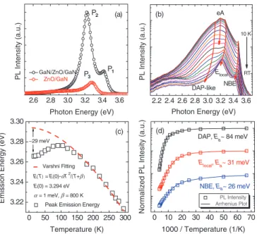
Figure2is the cross-section scanning electron microscopy (SEM) image of the GZG structure. According to the SEM image, GaN epilayer was indeed deposited on the ZG structure and some micro-air-voids can be observed in the ZnO layer. However, the thickness of ZnO epilayer is greatly reduced from the original 400–500 nm to about 150 nm. It could be believed that the diminution of the thickness is associated with the thermal decomposition of the ZnO epilayer. Simultaneously, the ZnO (11–20) reflection is seen only as a shoulder on the GaN (11–20) reflection profile, as shown in Fig.1b. Compared with the XRD data and SEM image, the ZnO layer indeed suffers from some damages such as the ZnO bonding decomposition and the ionized element diffusion effect during the GaN layer growth. Figure3ashows the PL spectra measured on the GZG and ZG structures at room temperature. Two obvious emission peaks measured from the spectra of the GZG structure lie at about 3.42 eV (P1) and
) unless CC License in place (see abstract). ecsdl.org/site/terms_use
address. Redistribution subject to ECS terms of use (see 140.113.38.11
Journal of The Electrochemical Society, 159 (3) H290-H292 (2012) H291 20 30 40 50 60 70 102 103 104 105 106 107 ( 1-102 ) r-plane Al2 O3 ( 11-20 ) ZnO ( 11-20 ) Ga N ( 2-204 ) r-plane Al2 O3 ZnO/GaN/r-sapphire X-ray Dif fraction Intensity (a.u. ) 2 Theta (degree) (a) 20 30 40 50 60 70 102 103 104 105 106 107 ( 440 ) ZnGa 2 O4 ( 1-10 2 ) r-p la ne Al2 O3 ( 2-20 4 ) r-p la ne Al2 O3 Cr ystalline Ga 2 O3 ( 11-20 ) Ga N ( 22 0 ) ZnGa 2 O4
X-ray Diffraction Intensity (a.u
.)
2 Theta (degree) GaN/ZnO/GaN/r-sapphire
(b)
Figure 1. XRD θ-2θ scans of a-plane (a) ZnO/GaN/r-sapphire and (b)
GaN/ZnO/GaN/r-sapphire structures.
3.22 eV (P2), respectively. It is so different from the PL spectrum
dominated by the 3.28 eV (P3) emission peak in the ZG structure. The
P3emission in the ZG structure is originated from the ZnO layer. Based
on these spectra, the P1 emission is clearly attributed to the optical
transition of the GaN layer. On the other hand, the related optical transitions of the P2 emission peak have been further clarified by
performing the temperature-dependent PL measurement ranging from 10 to 295 K, as shown in Fig.3b. In the low temperature, the emission peak at 3.476 eV corresponds to a-plane GaN near band-edge (NBE) emission consisted of two emission peaks assigned to donor-bound exciton (D0X) and free-exciton (FX) recombination, respectively.13If
we suppose the free exciton energy of GaN to be 3.476 eV at low temperature, the corresponding bandgap energy will be located at around 3.502 eV with an exciton binding energy of∼26 meV. This value is very close to the reported GaN fundamental bandgap energy of 3.503 eV at low-temperature by using the temperature dependence optical measurements.14
The P2 emission peak shifts to 3.265 eV as the temperature is
lowered to 10 K. Moreover, as the increasing temperature provides the thermal energy for ionized excitons dissociation, the P2emission
peak still dominates the PL spectrum even at the room temperature. The emission peak is attributed to the carrier localization (Elocal) at
the GaN/ZnO interface with a type II band configuration, which could be due to the formation of interface states and the excess charges from heterovalent bonding.15,16The S-shaped P
2emission peak
posi-tion variaposi-tion as a funcposi-tion of the temperature is a typical indicaposi-tion of the carrier localization behavior,17as shown in Fig.3c. Based on
these, the P2 should be assigned to the radiative recombination of
carriers localized at the interface. In addition, the low temperature emission peaks at about 3.192 eV and 3.106 eV decrease rapidly with increasing temperature, which are assigned to the band-to-acceptor (eA) transition and a donor-acceptor-pairs-like (DAP-like) transition, respectively. The zinc element diffusion phenomenon has been
ex-Figure 2. Cross-section SEM image of a-plane epitaxial GaN/ZnO/GaN
struc-ture. 2.6 2.8 3.0 3.2 3.4 3.6 P3 GaN/ZnO/GaN ZnO/GaN PL Intens ity (a.u.)
Photon Energy (eV)
P1 P2 (a) 2.2 2.4 2.6 2.8 3.0 3.2 3.4 3.6 RT 10 K Elocal DAP-like NBE (b) PL Int ensit y (a.u. )
Photon Energy (eV) eA 0 10 20 30 40 50 60 70 PL Intensity Arrhenius Plot NBE, Ea~ 26 meV Elocal, Ea~ 31 meV
Normalized PL Intesity (a.u.)
1000 / Temperature (1/K) DAP, Ea~ 84 meV (d) 0 50 100 150 200 250 300 3.22 3.24 3.26 3.28 3.30 ~29 meV α = 1 meV, β = 800 K E(0) = 3.294 eV Varshni Fitting
Peak Emission Energy
Emission Energy (eV)
Temperature (K) (c)
E(T) = E(0)-αT2/(T+β )
Figure 3. (a) Room-temperature (295 K) PL spectrum of the a-plane
GaN/ZnO/GaN structure. (b) Temperature-dependent PL spectra ranging from 10 K to 295 K measured from GaN/ZnO/GaN structure. (c) The PL peak energy of the carrier localization as a function of the temperature shows a well Varshni’s fitting for the experimental data. (d) The Arrhenius plots of the integrated PL intensities for the a-plane GaN/ZnO/GaN structure.
hibited in the XRDθ-2θ scan, and Zn impurity in GaN (ZnGa) could
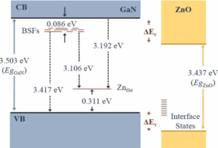
behave as the acceptor levels, or as p-type dopant in GaN. It is known that basal stacking faults (BSFs), the quite common defects in a-plane GaN-based materials, could be regard as the donors in this case, as a result of the high concentration of donors in the vicinity of BSFs.18
BSFs-related emission have also been demonstrated to locate at around 3.417–3.420 eV.13,19Moreover, the binding energy of Zn
Ga in GaN
has been determined to be about 0.34± 0.04 eV by simulation and ex-perimental measurement,20,21which is close to our experimental value
of 0.311 eV (= 3.503 eV−3.192 eV). The DAP-like emission energy at around 3.106 eV is almost consistent with the value obtained from the difference between the emission position of BSFs-induced donor-like levels and binding energy of ZnGaacceptors (3.417 eV−0.311 eV
= 3.106 eV).
Further the Arrhenius plots of the integrated PL intensities as a function of inverse temperature are summarized in Fig. 3d. The thermal activation energies can be determined by the equation,
I = I0/(1 + A exp(−Ea1/kT ) + B exp(−Ea2/kT )),
where Ea1 and Ea2 are the thermal activation energies at low and
high temperature regions, respectively. I0 is the PL intensity at low
temperature, and the coefficients A and B are the rate constants. The thermal activation energy of NBE emission is about 26 meV. This fitted value is assigned to the exciton binding energy of GaN and can correspond to our experimentally measured activation energy. For the transition of the carrier localization, the estimated value of thermal activation energy is about 31 meV, which is close to the localization energy of 29 meV by Varshni’s empirical formula, as shown in Fig.3c, and thus this value could be associated with the carrier delocalization energy with increasing temperature. The BSFs-induced donor level is located about 86 meV below the principle conduction band edge at 10 K, which is close to the fitted value of thermal activation energy of DAP-like transition (about 84 meV). Thus, we can reasonably attribute that thermal activation energy for quenching of DAP-like transition could be the thermal ionization energy of the BSFs-induced donor. Based on the optical measurement results at low temperature, the related energy levels and corresponding optical transitions in a-plane GZG structure are sketched in Fig.4.
) unless CC License in place (see abstract). ecsdl.org/site/terms_use
address. Redistribution subject to ECS terms of use (see 140.113.38.11
H292 Journal of The Electrochemical Society, 159 (3) H290-H292 (2012)
Figure 4. Energy diagram showing the energy levels of Zn-induced acceptors
in the a-plane GaN on ZnO heterointerface.
In summary, a-plane GaN/ZnO/GaN heterostructure has been fab-ricated by the expitaxial growth techniques, and their optical properties have also been clarified and summarized. The strong emission peak position at around 3.22 eV at room temperature corresponds to the car-rier localization at the GaN/ZnO interface. The out-diffusion behavior of Zn atom greatly affects the optical properties of GaN/ZnO, and the binding energy of ZnGaacceptors is estimated to be about 0.311 eV in
the a-plane heterostructure. The GaN/ZnO heterostructure is expected to exhibit a significant effect on the recombination at the interface and energy level alignment, and consequently the optoelectronic device application.
Acknowledgments
The author thank Professor. H. C. Kuo and Professor S. C. Wang in Department of Photonics of National Chiao Tung University for their great technical support. This work was supported by the MOE ATU
program and in part by the National Science Council of Republic of China (ROC) in Taiwan under contract NSC-99-2120-M-009-007 and NSC 99-2221-E-009-035-MY3.
References
1. P. Yang, H. Yan, S. Mao, R. Russo, J. Johnson, R. Saykally, N. Morris, J. Pham, R. He, and H. J. Choi,Adv. Funct. Mater., 12(5), 323 (2002).
2. Z. L. Wang and J. Song,Science, 312, 242 (2006).
3. Ya. I. Alivov, J. E. Van Nostrand, D. C. Look, M. V. Chukichev, and B. M. Ataev,
Appl. Phys. Lett., 83, 2943 (2003).
4. Q. X. Yu, B. Xu, Q. H. Wu, Y. Liao, G. Z. Wang, R. C. Fang, H. Y. Lee, and C. T. Lee,Appl. Phys. Lett., 83, 4713 (2003).
5. D. K. Hwang, S. H. Kang, J. H. Lim, E. J. Yang, J. Y. Oh, J. H. Yang, and S. J. Park,
Appl. Phys. Lett., 86, 222101 (2005).
6. N. Li, E. H. Park, Y. Huang, S. Wang, A. Valencia, B. Nemeth, J. Nause, and I. Ferguson,Proc. of SPIE, 6337, 63370Z (2006).
7. S. J. Wang, N. Li, E. H. Park, Z. C. Feng, A. Valencia, J. Nause, M. Kane, C. Summers, and I. Ferguson,Phys. stat. sol. (c), 5(6), 1736 (2008).
8. X. Gu, M. A. Reshchikov, A. Teke, D. Johnstone, H. Morkoc, B. Nemeth, and J. Nause,Appl. Phys. Lett., 84, 2268 (2004).
9. A. Kobayashi, Y. Kawaguchi, J. Ohta, H. Fujioka, K. Fujiwara, and A. Ishii,Appl. Phys. Lett., 88, 181907 (2006).
10. P. Waltereit, O. Brandt, A. Trampert, H. T. Grahn, J. Menniger, M. Ramsteiner, M. Reiche, and K. H. Ploog,Nature, 406, 865 (2000).
11. A. Kobayashi, S. Kawano, Y. Kawaguchi, J. Ohta, and H. Fujioka,Appl. Phys. Lett., 90, 041908 (2007).
12. A. Kobayashi, S. Kawano, K. Ueno, J. Ohta, H. Fujioka, H. Amanai, S. Nagao, and H. Horie,Appl. Phys. Lett., 91, 191905 (2007).
13. P. P. Paskov, R. Schifano, B. Monemar, T. Paskova, S. Figge, and D. Hommel,
J. Appl. Phys., 98, 093519 (2005). 14. B. Monemar,Phys. Rev. B, 10, 676 (1974).
15. T. Nakayama and M. Murayama,J. Cryst. Growth, 214/215, 299 (2000). 16. A. M. C. Ng, Y. Y. Xi, Y. F. Hsu, A. B. Djuriˇsi´c, W. K. Chan, S. Gwo, H. L. Tam,
K. W. Cheah, P. W. K. Fong, H. F. Lui, and C. Surya,Nanotechnology, 20, 445201 (2009).
17. Y. H. Cho, G. H. Gainer, A. J. Fischer, J. J. Song, S. Keller, U. K. Mishra, and S. P. DenBaars,Appl. Phys. Lett., 73, 1370 (1998).
18. P. Corfdir, P. Lefebvre, J. Risti´c, J. D. Gani`ere, and B. Deveaud-Pl´edran,Phys. Rev. B, 80, 153309 (2009).
19. P. Corfdir, P. Lefebvre, J. Levrat, A. Dussaigne, J. D. Ganie`re, D. Martin, J. Ristic´, T. Zhu, N. Grandjean, and B. D. Ple´dran,J. Appl. Phys., 105, 043102 (2009). 20. M. Monemar, H. P. Gislason, and O. Lagerstedt,J. Appl. Phys., 51, 640 (1980). 21. N. Nepal, M. L. Nakarmi, H. U. Jang, J. Y. Lin, and H. X. Jiang,Appl. Phys. Lett.,
89, 192111 (2006).
) unless CC License in place (see abstract). ecsdl.org/site/terms_use
address. Redistribution subject to ECS terms of use (see 140.113.38.11