Wet-milled transition metal oxide nanoparticles as buffer layers for bulk
heterojunction solar cells{
Jen-Hsien Huang,{
aTzu-Yen Huang,{
bHung-Yu Wei,
cKuo-Chuan Ho
bcand Chih-Wei Chu*
ad Received 26th March 2012, Accepted 12th June 2012DOI: 10.1039/c2ra20543b
In this study, we used high-energy grinding to prepare solutions of well-dispersed transition metal oxides (TMOs), allowing the fabrication of crystalline TMO films with high surface coverage through solution processing without post-annealing. Moreover, because this solution-based method did not require surfactants, it preserved the intrinsic electronic and optical properties of the TMOs. The resulting smooth, continuous, and highly transparent TMO films were readily integrated into organic solar cells. After incorporating MoO3thin films into bulk heterojunction solar cells, we obtained devices delivering power conversion efficiencies of up to 3.68%, rivalling those of devices fabricated with commercial poly(3,4-ethylenedioxythiophene):polystyrenesulfonate (PEDOT:PSS) as the hole collection layer.
1. Introduction
Polymer photovoltaic cells offer great technological potential as renewable, alternative sources of electrical energy, with the attractions of low-cost fabrication, low specific weight, and mechanical flexibility. Since solution-processed bulk heterojunc-tion (BHJ) solar cells were first reported in the mid-1990s, they have been the subject of intense research interest because of their ease of processing and the superior mechanical properties (e.g., flexibility) imparted by the polymers. Recently, some low-bandgap conjugated polymers have exhibited very high power conversion efficiencies (PCEs) as a result of their wide spectral coverages; such systems have great commercial potential.1–3 Further attempts at improving these PCEs have been based on tandem cell structures and the development of low-bandgap materials.4,5 Such tandem cells do, however, require a stable, transparent, solvent-resistant intermediate layer; moreover, stability remains a problem and limits their practical applica-tions. In general, the buffer layer or intermediate layer in a BHJ device is the most sensitive to humidity. The poor long-term stability of BHJ devices usually arises from an unstable buffer layer. Therefore, the development of an air-stable, solution-processed buffer layer is a potentially rewarding challenge.
Transition metal oxides (TMOs) have attracted much atten-tion for their unique electronic, magnetic, and optical properties. Most importantly for application in polymer photovoltaic cells, TMOs are much more environmentally stable than organic materials. They are readily deposited as thin films exhibiting good physical adhesion, transparency in the visible range, and superior stability. These properties make them promising materials for integration into optoelectronic devices. Recently, some TMOs, including WO3, V2O5, and MoO3, have been successfully employed as buffer layers in organic solar cells.6–10 The inserted layer of metal oxides can modify the work function of indium tin oxide (ITO) to enhance hole injection, thereby leading to improved cell performance.
Thermal evaporation under high vacuum is the most common method for depositing TMO films. This approach can produce high-quality TMO films with smooth morphologies and good surface coverage. Large-scale, high-throughput production of solar cells would, however, favor the use of solution processing of the buffer layer. Recently, sol–gel routes have been proposed as alternative syntheses of TMO films,11–13 allowing mass production without the need for high vacuum conditions. The major drawbacks of the sol–gel method are the complexity of the reaction and the incorporation of impurities during the synthetic process; moreover, the prepared TMO films are usually amorphous structures. To remove chemical impurities or achieve crystalline phases in such TMO films, it is necessary to perform post-annealing at high temperatures—not only increasing the product cost but also restricting the range of applicable substrates. In light of these issues, some groups have dispersed TMO nanoparticles with polymers as surfactants to prepare stable suspensions;14 these solutions can be cast onto various substrates, forming crystalline TMO films at relatively low temperatures. After deposition, the polymeric dispersant can be
a
Research Center for Applied Sciences, Academia Sinica, Taipei, 11529, Taiwan
b
Department of Chemical Engineering, National Taiwan University, Taipei, 10617, Taiwan
c
Institute of Polymer Science and Engineering, National Taiwan University, Taipei, 106, Taiwan
dDepartment of Photonics National Chiao Tung University, Hsinchu, 300,
Taiwan
{Electronic Supplementary Information (ESI) available. See DOI: 10.1039/c2ra20543b
{Both authors contributed equally to this paper.
Cite this: RSC Advances, 2012, 2, 7487–7491
www.rsc.org/advances
PAPER
removed through oxygen plasma treatment. In this present study, we used a wet grinding method to disperse the TMO in isopropyl alcohol. During the grinding process, the sizes of the TMO particles decreased significantly, forming a stable colloidal solution. This surfactant-free, large-scale solution process preserved the intrinsic electronic properties of the TMO; in addition, this clean, solution-processable, low-temperature method provided high-quality TMO films without the need for any organic compounds.
2. Experimental
High-purity crystalline TMO powders (99.99%, Aldrich) and isopropyl alcohol were used as the starting material and solvent, respectively. High-energy ball milling was performed at a speed of 2000 rpm at room temperature using a batch-type grinder (JBM-B035). The milling duration was typically between 30 and 360 min; the concentration of TMOs was 0.1 wt%. After high-energy grinding, the TMO suspensions could be diluted to any concentration without precipitation.
The fabrication of the devices was initiated by cleaning the ITO-coated glass and then exposing the substrates to UV-ozone for 15 min. For the preparation of inverted cells, a TMO solution having a concentration of 0.01 wt% was spun onto the ITO
substrates, which were subsequently dried at 120 uC for 1 h. Next, a ‘‘slow-grown’’ layer of P3HT : PCBM (1 : 1, w/w; 2% in dichlorobenzene) was cast upon the TMO buffer layer.15Finally, thermal evaporation of Ca and Al provided the reflective anodes. Particle sizes and zeta potentials were measured using a particle size analyzer (Brookhaven 90 Plus Sn11408). The absorption spectra were obtained using a Jasco-V-670 UV-Vis spectrophotometer. XRD was performed using a Philips X’Pert/ MPD apparatus. The surface morphologies of the polymer films were investigated using AFM (Digital Instrument NS 3a controller equipped with a D3100 stage) and SEM (Hitachi S-4700). XPS/UPS spectra were recorded using a PHI 5000 VersaProbe (ULVAC-PHI, Chigasaki, Japan) system. The cell performance was tested under simulated AM 1.5 G irradiation at 100 mW cm22using a Xe lamp-based solar simulator (Thermal Oriel 1000 W). The light intensity was calibrated using a mono-silicon photodiode equipped with a Hamamatsu KG-5 color filter. The whole measurement process was performed at room temperature in a N2-filled glove box.
3. Results and discussion
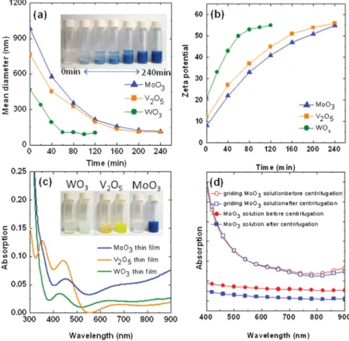
In this study, we used a grinding method to prepare solutions of MoO3, V2O5, and WO3. Fig. 1a reveals that the particle sizes of
Fig. 1 Plots of (a) the average particle sizes of the TMOs with respect to the grinding time (inset: photographs of the MoO3solutions after different
grinding times); (b) the zeta potentials of the TMO solutions with respect to grinding time; (c) the absorbance of the TMO films cast from the as-prepared solutions (inset: photograph of the TMO solution before and after grinding for 240 min); and (d) the absorbance of the MoO3solution before
and after centrifugation at 5000 rpm.
the three TMOs decreased significantly upon increasing the grinding time. In the case of MoO3, the average particle size decreased from 468 to 105 nm after grinding for 4 h. During the grinding procedure, the TMO particles experienced de-aggrega-tion and physical dissociade-aggrega-tion into smaller particles, due to plastic deformation. Notably, after grinding for 4 h, the smaller particles of the TMOs could be fully dispersed, forming stable suspensions. To investigate the correlation between the particle size and the dispersibility of these TMOs, we measured the zeta potentials of the TMO solutions after various grinding times. Fig. 1b reveals that the zeta potentials increased after grinding, indicating that the smaller particles were more highly charged, thereby enhancing the dispersibility of the TMO solutions. Fig. 1c displays the absorbencies of the as-prepared TMO solutions; the solutions were stable, without precipitation, for over 3 months (see the insets to Fig. 1c for images of the TMO solutions before and after grinding). Fig. 1d presents the solution absorbencies before and after centrifugation. Without grinding, the MoO3solution exhibited a broad absorbance in the visible range without any peaks, suggesting that the MoO3 powder could not be dispersed; indeed, the absorbance decreased significantly after centrifugation. In contrast, the MoO3sample obtained after grinding exhibited a strong absorbance at wavelengths beyond 500 nm, indicating that the nanoscale MoO3powder was fully dispersed. Moreover, the absorbance of the ground MoO3remained almost identical after centrifugation at 5000 rpm, suggesting that its dispersibility was very good.
The surface roughness of the buffer layer in an organic solar cell is a critical feature. An extremely large roughness would affect device fabrication if some of the buffer layer were to protrude through the active layers, thereby resulting in a short circuit. Therefore, we used atomic force microscopy (AFM) and scanning electron microscopy (SEM) to monitor the surface roughness and morphologies of buffer layers cast from the as-prepared TMO solutions. Fig. 2 displays AFM images of the bare ITO and TMO films. All of the TMO films exhibited good
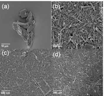
surface coverage without any obvious aggregation. The calcu-lated root mean square roughness of the films of MoO3, V2O5, and WO3 were 7.3, 9.2, and 8.4 nm, respectively—almost the same as that of the bare ITO substrate. Fig. 3 presents SEM images revealing the changes in the MoO3 morphology with respect to the grinding time. Prior to grinding, the MoO3powder could not be processed to form a thin film; in contrast, the ground samples could form continuous films. After longer grinding times, the morphology of the cast film became smoother. The corresponding SEM images of the V2O5 and WO3 powders before and after grinding are provided in the Supporting Information (Fig. S1{).
Fig. 4 XRD patterns of the TMO powders before and after grinding for 240 min.
Fig. 2 AFM images of (a) the bare ITO substrate and the (b) MoO3, (c)
V2O5, and (d) WO3films. Scale bar: 400 nm.
Fig. 3 SEM images of the MoO3powders (a) prior to grinding and (b–
d) after grinding for (b) 120, (c) 180, and (d) 240 min.
To study the effect of grinding on the material structure, we used X-ray diffraction (XRD) to analyze the crystalline structures of the TMOs. Fig. 4 reveals simultaneous decreases in intensity and broadening of the signals in the XRD spectra of the three TMOs, indicating decreases in crystallinity. These features are consistent with decreases in the grain size and lattice strain induced by high-energy grinding. From the widths of the XRD peaks and Scherrer’s equation,16we determined the crystallite grain sizes of the MoO
3, V2O5, and WO3powders to be 254, 165, and 98 nm, respectively, prior to grinding; these values decreased to 87, 54, and 47 nm, respectively, after grinding. The XPS spectrum of MoO3 film is presented in the Supporting Information (Fig. S2{). Because this solution-based method did not require any surfactants, the chemical composition of the film was dependent only upon that of the pure MoO3powder. Therefore, this method preserved the intrinsic electronic properties of the TMOs.
The most important requirement for a buffer layer in a solar cell is alignment of energy levels. For efficient hole collection
from the organic electron donor to the anode electrode, the work function of the buffer layer must match the energy level of the highest occupied molecular orbital (HOMO) of the organic material. Here, we applied the UPS technique to measure the valence band edge of the TMO film cast from each dispersed solution. Based on the upper (E1) and lower (E2) emission onset energy levels of the secondary photoelectrons from the TMO films, we estimated the work function using the equation
w= hv 2 (E12 E2)
For MoO3, V2O5, and WO3, the values of E1were 16.4, 16.0, and 16.5 eV, respectively, and those of E2 were 2.6, 2.5, and 2.65 eV, respectively (Fig. 5). Therefore, the valence band edges for MoO3, V2O5, and WO3 were 7.4, 7.7, and 7.35 eV, respectively. These values are in very good agreement with those reported using other techniques.17–20These values for the TMO films are larger than the work function of poly(3,4-ethylenediox-ythiophene):polystyrenesulfonate (PEDOT:PSS) (5.2 eV), making them much more suitable for modern high-efficiency copolymer systems featuring very deep HOMO energy levels.
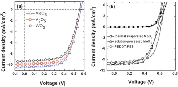
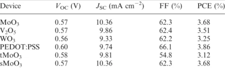
To determine the hole collection capabilities of the solution-processed TMO films, we incorporated these TMO films into conventional BHJ solar cell devices based on P3HT and PCBM. Fig. 6a displays the current density–voltage (J–V) characteristics of representative devices; Table 1 lists the average device parameters (from a minimum of three devices). Among these three TMO films, the MoO3 film delivered the highest short-circuit current (JSC) of 10.36 mA cm22; with an open-circuit voltage (VOC) of 0.57 V and a fill factor (FF) of 62.3%, the power conversion efficiency (PCE) was 3.68%. The highest values of JSC for the MoO3-based devices was likely due to their greater surface coverage and lower roughness, leading to superior hole collection properties. We also studied the effect of the grinding time and the solution concentration on the performance of the MoO3-based devices (Fig. S3, Supporting Information{). Fig. 6b compares the performances of the devices based on solu-tion-processed MoO3 (sMoO3), thermally evaporated MoO3
Fig. 6 Cell performances of P3HT:PCBM BHJ solar cells incorporating (a) different metal oxides as hole collection layers and (b) different types of buffer layers.
Fig. 5 The UPS spectra for the MoO3, V2O5and WO3films cast from
the as-prepared solutions.
(tMoO3), and commercial PEDOT:PSS, which provided PCEs of 3.68, 3.12, and 3.86%, respectively. The slightly higher PCE for the PEDOT:PSS-based device was due to its larger FF. These data suggest that both the thermally evaporated and solution-processed MoO3 films could be used as substitutes for PEDOT:PSS buffer layers between the ITO and the polymer layer, with comparable device performance.
4. Conclusion
In conclusion, we have developed a low-temperature, rapid, solution-processed route for the production of thin, continuous TMO films for the hole collection layer in organic solar cells. During the grinding process, a TMO powder is transformed into smaller particles, thereby increasing the zeta potential and improving the dispersibility. With the crystalline TMO films as the hole collection layer, the devices can produce PCEs compar-able with those of standard devices featuring PEDOT:PSS as the buffer layer. Such highly dispersed TMO solutions might also be suitable for application as intermediate layers for organic tandem cells, hole injection layers in organic light emitting diodes, and active layers for electrochromic devices.
Acknowledgements
We thank the National Science Council (NSC), Taiwan (NSC 100-2221-E-001-009-), and the Thematic Project of Academia Sinica, Taiwan (AS-100-TP-A05), for financial support.
References
1 G. Zhao, Y. He and Y. Li, Adv. Mater., 2010, 22, 4355.
2 M. K. Siddiki, J. Li, D. Galipeau and Q. Qiao, Energy Environ. Sci., 2010, 3, 867.
3 D. Gendron and M. Leclerc, Energy Environ. Sci., 2011, 4, 1225. 4 J. Yang, J. You, C. C. Chen, W. C. Hsu, H. R. Tan, X. W. Zhang, Z.
Hong and Y. Yang, ACS Nano, 2011, 5, 6210.
5 J. Yang, R. Zhu, Z. Hong, Y. He, A. Kumar, Y. Li and Y. Yang, Adv. Mater., 2011, 23, 3465.
6 M. Vasilopoulou, L. C. Palilis, D. G. Georgiadou, P. Argitis, S. Kennou, I. Kostis, G. Papadimitropoulos, N. A. Stathopoulos, A. A. Iliadis, N. Konofaos, D. Davazoglou and L. Sygellou, Thin Solid Films, 2011, 519, 5748.
7 C. Gong, H. B. Yang, Q. L. Song and C. M. Li, Org. Electron., 2012, 13, 7.
8 S. Schumann, R. Da Campo, B. Illy, A. C. Cruickshank, M. A. McLachlan, M. P. Ryan, D. J. Riley, D. W. McComb and T. S. Jones, J. Mater. Chem., 2011, 21, 2381.
9 H. Cheun, J. D. Berrigan, Y. Zhou, M. Fenoll, J. Shim, C. Fuentes-Hernandez, K. H. Sandhage and B. Kippelen, Energy Environ. Sci., 2011, 4, 3456.
10 J. Sakai, K. Kawano, T. Yamanari, T. Taima, Y. Yoshida, A. Fujii and M. Ozaki, Sol. Energy Mater. Sol. Cells, 2010, 94, 376. 11 K. Zilberberg, S. Trost, H. Schmidt and T. Riedl, Adv. Energy
Mater., 2011, 1, 377.
12 K. Zilberberg, S. Trost, J. Meyer, A. Kahn, A. Behrendt, D. Lu¨tzenkirchen-Hecht, R. Frahm and T. Riedl, Adv. Funct. Mater., 2011, 21, 4776.
13 J. H. Huang, H. Y. Wei, K. C. Huang, C. L. Chen, R. R. Wang, F. C. Chen, K. C. Ho and C. W. Chu, Energy Environ. Sci., 2010, 3, 654. 14 J. Meyer, R. Khalandovsky, P. Go¨rrn and A. Kahn, Adv. Mater.,
2011, 23, 70.
15 G. Li, V. Shrotriya, J. Huang, Y. Yao, T. Mariarty, K. Emery and Y. Yang, Nat. Mater., 2005, 4, 864.
16 P. Scherrer, GA¨ottinger Nachrichten, 2, 98, 1918; cf. also Kolloidchemie, ed. R. Zsigmondy, Sparner, Leipzig, 3rd edn, 1920, p. 394.
17 M. Merz, J. Eisenmenger, B. Heinz and P. Ziemann, Phys. Rev. B: Condens. Matter, 2002, 66, 184102.
18 K. J. Lethy, D. Beena, R. V. Kumar, V. P. M. Pillai, V. Ganesan, V. Sathe and D. M. Phase, Appl. Phys. A: Mater. Sci. Process., 2008, 91, 637.
19 M. Kro¨oger, S. Hamwi, J. Meyer, T. Riedl, W. Kowalsky and A. Kahn, Org. Electron., 2009, 10, 932.
20 J. Meyer, K. Zilberberg, T. Riedl and A. Kahn, J. Appl. Phys., 2011, 110, 033710.
Table 1 Device operation parameters of cells incorporating the different types of buffer layers fabricated in this study
Device VOC(V) JSC(mA cm 22 ) FF (%) PCE (%) MoO3 0.57 10.36 62.3 3.68 V2O5 0.57 9.86 62.4 3.51 WO3 0.56 9.33 62.2 3.25 PEDOT:PSS 0.60 9.74 66.1 3.86 tMoO3 0.58 9.81 54.8 3.12 sMoO3 0.57 10.36 62.3 3.68