Testing Methodology of Embedded DRAMs
Hao-Yu Yang, Chi-Min Chang, Mango C.-T. Chao, Rei-Fu Huang, and Shih-Chin Lin
Abstract—The embedded-DRAM (eDRAM) testing mixes up the
techniques used for DRAM testing and SRAM testing since an eDRAM core combines DRAM cells with an SRAM interface (the so-called 1T-SRAM architecture). In this paper, we first present our test algorithm for eDRAM testing. A theoretical analysis to the leakage mechanisms of a switch transistor is also provided, based on that we can test the eDRAM at a higher temperature to reduce the total test time and maintain the same retention-fault coverage. Finally, we propose a mathematical model to estimate the defect level caused by wear-out defects under the use of error-correc-tion-code circuitry, which is a special function used in eDRAMs compared to commodity DRAMs. The experimental results are col-lected based on 1-lot wafers with an 16 Mb eDRAM core.
Index Terms—Embedded-DRAM (eDRAM), fault model,
reten-tion, error-correction-code.
I. INTRODUCTION
D
UE to the advantages of high density, structure simplicity, low-power consumption, and low cost, DRAM has been the mainstream of the commodity-memory market since its invention by Dr. Dennard [1]. With the continually growing need to an effective and economic embedded-memory core in the SoC era, researchers attempt to carry DRAM’s advantages from a commodity memory into a SoC. In the past decade, a lot research effort has been put into the embedded-DRAM (eDRAM) technologies, such as deep-trench capacitor with bottle etch [2], planar capacitor [3], [4], shallow trench capac-itor [4], and metal-insulator-metal (MIM) capaccapac-itor [3], [5], to reduce the process adders to the CMOS process, where the eDRAM is embedded in. The eDRAM technologies are now available in the IC-foundry industry [6], [7] and its applications include the products of networking, multimedia handheld de-vices, gaming consoles, high definition television, and so forth. Unlike integrating a bare DRAM die within a system-in-package or a system-in-packaged DRAM on a system board, where the responsibility of testing the commodity DRAM itself is on the memory design company, the responsibility of testing the eDRAM is transferred to the system integrator. Testing large embedded-memory cores has been a big challenge for Manuscript received October 22, 2010; revised February 27, 2011; accepted June 13, 2011. Date of publication August 12, 2011; date of current version July 05, 2012.H.-Y. Yang, C.-M. Chang, and M. C.-T. Chao are with the Department of Electronics Engineering and Institute of Electronics, National Chiao Tung University, Hsinchu 300, Taiwan (e-mail: [email protected]; [email protected]; [email protected]).
R.-F. Huang is with the MediaTek Inc., Hsinchu 300, Taiwan (e-mail: [email protected]).
S.-C. Lin is with the United Microelectronics Corporation, Hsinchu 300, Taiwan (e-mail: [email protected]).
Color versions of one or more of the figures in this paper are available online at http://ieeexplore.ieee.org.
Digital Object Identifier 10.1109/TVLSI.2011.2161785
SoC testing due to the difficulty of test isolation and test accessibility [8]. By reducing the tester requirement and en-abling the parallel testing of different memory cores, memory built-in-self-test (BIST) circuit is the best solution to the em-bedded memory testing in common consensus today [9]–[11]. Several BIST schemes are proposed for the embedded DRAM testing [12]–[15]. However, these previous works mainly focus on the architecture and the automatic generation of the BIST circuitry. Few discussions on the test algorithms and the test-time overhead resulted from the retention test can be found in the literature for the eDRAM testing.
The conventional DRAM testing contains two main tasks: the retention testing and the functional testing. In the reten-tion testing, we test whether the data retenreten-tion time of each DRAM cell can meet its specification. In the functional testing, we test whether the DRAM-cell array and its peripheral cir-cuits can function correctly at different operating modes, which combine different cycle latencies with different clock frequen-cies for special applications, such as the burst mode and page read/write. To cover various fault models for the DRAM array, several test algorithms, such as checkerboard, address comple-ment, March, row/column disturb, self-refresh, XMOVI, and butterfly, need to be applied. Applying all the above algorithms at different operating modes is time-consuming, and hence, in reality, most DRAM companies prize their DRAM chips dif-ferently according to the length of the applied test. With this price model, DRAM companies need to analyze their process as well as their memory design to rank the fault models by their possibility of occurrence. Then, the test engineers can choose a proper combination of test algorithms to cover the high-ranked faults as much as possible when the length of the applied test is limited.
In fact, testing eDRAMs is quite different from testing commodity DRAMs due to the following reasons. First of all, most eDRAM macros use the SRAM interface (the so-called 1T-SRAM architecture), which consists of no address multi-plexer (no CAS, RAS) and can auto-refresh. Second, unlike commodity DRAM, whose application might be unknown before the fabrication, eDRAM macros are more applica-tion-specific and hence have only one operating mode, meaning that one cycle latency at only one operating frequency needs to be tested. Due to the use of a simple SRAM interface in eDRAMs, testing eDRAMs is more like testing SRAMs and requires a shorter test algorithm than testing commodity DRAMs. However, testing eDRAM is not as simple as testing SRAMs since some fault models which may not occur in SRAMs, such as retention faults and coupling faults, may occur in eDRAM. Third, the process of eDRAMs is different from that of commodity DRAMs, meaning that their storage capacitors, bit lines, word lines, transistors models, number of metal layers, and wire models are all different. As a result, 1063-8210/$26.00 © 2011 IEEE
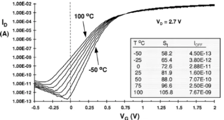
Fig. 1. Relation between and associated with different temperatures [17].
the possibility of a fault’s occurrence for eDRAMs is different from that for commodity DRAMs as well.
Similar to commodity DRAMs, eDRAMs require a retention test as well. The specification of eDRAM’s data-retention time is a constant and usually in the order of milliseconds. As a result, the ratio of this retention test time over the eDRAM test time in-creases when the clock frequency of the eDRAM inin-creases. It implies that the retention-test time may dominate the eDRAM test time for high-performance eDRAM designs. The data-re-tention time of an eDRAM cell depends on the leakage cur-rent of the switch transistor in the cell, which is sensitive to the temperature [16], [17]. Fig. 1 shows that a transistor’s leakage current increases dramatically with the increase of temperature [17]. Therefore, by properly increasing the test temperature, the retention test time can be significantly reduced.
Furthermore, unlike commodity DRAM utilizing spare rows and columns for repair, most eDRAM macros utilize error cor-rection code (ECC) circuitry to improve their yield as well as its reliability since eDRAM’s storage capacitor is small and thus more susceptible to the noise, soft errors, or wear-out defects. Because some wear-out defects might be masked by the ECC circuitry, we need to turn off the ECC circuitry and collect the raw defect statistics of the eDRAM macros when applying the reliability testing, such as temperature, humidity, bias (THB) test [18], highly-accelerated temperature and humidity stress (HAST) test [19], and high temperature operating life (HTOL) test [20]. Then, how to estimate the defect level based on the collected raw defect statistics becomes an interesting but prac-tical problem for eDRAMs.
In this paper, we would like to share our experience in testing an UMC 65 nm eDRAM macro. We first discuss the test al-gorithms used for the eDRAM testing and compare the corsponding yields of different test algorithms through silicon re-sult. We then analyze the test time of eDRAM retention test and its ratio to total eDRAM test time. Next, we study the leakage mechanisms of a switch transistor and theoretically compute the leakage-charge equivalence between different temperatures. Based on this leakage-charge equivalence, we can obtain the equivalent retention time used for retention test at different tem-peratures. We also report the test-time reduction by increasing tester’s temperature and validate the equivalent retention-fault coverage through silicon result. In addition, we further discuss how reliability testing can help to identify the wear-out defects
Fig. 2. Embedded-DRAM architecture.
and then develop an efficient mathematical model to estimate the defect level resulting from the wear-out defects based on the use of ECC, which is a special function used in eDRAMs compared to commodity DRAMs.
The remainder of this paper is organized as follows. Section II first introduces the embedded DRAM architecture in use. Section III presents a reduced, effective test algorithm for eDRAMs. Section IV discusses the leakage mechanism of a switch transistor and analyzes the retention-test time at different temperatures. Section V discusses the defect level resulting from the wear-out defects when ECC is used. The conclusion is given in Section VI.
II. BACKGROUND
A. Overview of Embedded DRAM
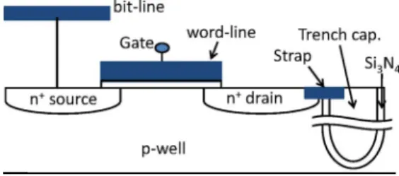
Fig. 2 shows the block diagram of a 16 Mb eDRAM macro used in our SoC design. This eDRAM macro utilizes deep trench capacitors and is implemented in a UMC 65 nm low-leakage logic process. Fig. 3 shows a cross-section view of an eDRAM cell in our design. The word size on the interface of this eDRAM macro is 32 bits. Due to the use of ECC, we need to add 6-bit more memory cells to the physical array for each word, and hence the physical data stored in the memory array is 38 bits per word. A physical 38-bit word is read out from or written into the memory array through the ECC circuitry, which encodes a 32-bit word into a 38-bit word or decodes a 38-bit word to a 32-bit word. The size of the eDRAM macro is around 4 mm , which contains two symmetric eDRAM arrays. Each array con-tains 128 banks, and each bank concon-tains 64 word-lines and its own local sense amplifier. Each word-line on each array is con-nected to 64 half-words, and the data-width of each half-word is 19 bits. Note that the layout topology of the eDRAM array utilizes the distributed folding scheme, where the th bit of the th word is adjacent to the th bit of the th word, not the th bit of the original th word. Between the two eDRAM arrays is the address decoder including word-line drivers. The
Fig. 3. Illustration of an eDRAM cell.
Fig. 4. Exemplary array scrambling.
control circuit (CTL) and global sense amplifier (GSA) are on the bottom of the eDRAM core.
The CTL controls all operations of eDRAM, including read, write, self-refresh, auto-refresh, and any application-dependent operation such as burst-mode read/write or byte read/write. After precharge and charge redistribution, the data is first dif-ferentiated by LSA, then passed to GSA, and read out through the read/write path. The refresh operation in this eDRAM core can be finished by using the LSA so that refreshing all the words on one word-line (64 words in total) requires only one cycle. Therefore, total 64 128 cycles are required for one refresh operation. When operating at 100 MHz, the bandwidth of this eDRAM core is 3.125 Gb/s (32 bits 100 MHz).
In modern memory designs, scrambling techniques are com-monly used to optimize memory’s layout geometry, address decoder, cell area, performance, yield, and I/O pin compatibility [21]. The types of scrambling include folding, address decoder scrambling, contact and well sharing, and bit-line twisting. Fig. 4 shows an exemplary scrambling used in our eDRAM design, where the ordering of word-lines in this example is arranged according to the least significant bits of the address. With an SRAM interface, eDRAM utilizes both bit-lines and bit-line-bars to distinguish the data value stored in an eDRAM cell, but a cell’s data is only connected to either one of the corresponding bit-line and bit-line-bar. In this example, each word-line connects to two 4-bit words. The first word on a word line uses the 0th, 2nd, 4th, and 6th pairs of the bit-line and bit-line-bar, and the second word uses the 1st, 3rd, 5th, and 7th pairs. By proper arrangement, half of eDRAM cells are connected to bit-line, and the other half to the bit-line-bar.
TABLE I
WRITE-OPERATIONSEQUENCE ANDCORRESPONDINGFUNCTIONALINPUTS FORFILLING THECHECKERBOARDBACKGROUND INFIG. 4
As a result, the physical value of those cells connected to a bit-line-bar is inverse to their logical value. In addition, the bit-line twist for a column reverses the physical-value/log-ical-value relation of the cells below that twist.
During the eDRAM testing, the data background written into or read from the memory macro should represent cell’s physical value instead of its logical value. Therefore, when designing the BIST circuitry, we need to build a scramble table to map the physical value described in the test algorithm to its corresponding logical value for a given address [21], [22]. Those logical values then form the functional test patterns or expected responses during testing. This scramble table can be implemented by a simple two-level logic, whose inputs contain few least significant bits and most significant bits of an address. In addition, when performing March algorithm, the sequence of the activated word-lines also needs to follow the physical sequence, not logical address sequence. Thus, the BIST requires another physical-address-mapping circuitry to handle this address scrambling. For instance, Fig. 4 shows a checkerboard background for cells’ physical values. To fill such a background with an -direction March algorithm, the sequence of write operations and the corresponding functional inputs are listed in Table I.
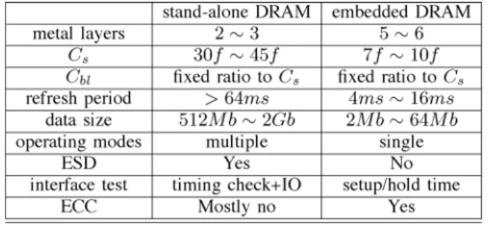
B. Difference Between eDRAM and Commodity DRAM Table II compares the eDRAMs with the commodity DRAMs. First of all, the array structure and the peripheral circuits of commodity DRAMs are both simple and hence a commodity-DRAMs process usually requires two or three metal layers. On the other hand, eDRAMs are integrated into a logic process, which usually uses five or more metal layers.
Second, the storage capacitor in commodity DRAMs
is larger than that of eDRAMs since a commodity-DRAM process is developed specifically for DRAM cells. Third, the read mechanism of DRAMs is based on the charge sharing between the storage capacitor and the bit-line’s capacitor . Thus, the length of the bit-line is limited by the ratio
TABLE II
COMPARISONBETWEENCOMMODITYDRAMS ANDEMBEDDEDDRAMS
a successful read operation through the sense amplifier. In our eDRAM design, this ratio is set to 15 . Since the of commodity DRAMs is larger than that of eDRAMs, the bit-line in commodity DRAMs is also longer, meaning more bit cells per bit-line for commodity DRAMs. Also, the refresh period for commodity DRAMs is longer since a larger can tolerate more leakage. In addition, the word-line, which is implemented by polysilicon, is longer in eDRAMs because the extra metal layers in the logic process can be used to reduce word-line’s resistance by connecting the word-line in parallel.
From testing’s point of view, the eDRAM testing is simpler than the commodity-DRAM testing. First, the data size of eDRAM is smaller, and hence requires shorter test application time. Second, commodity DRAMs have multiple operating modes, i.e., several difference latency cycles mix with several clock frequencies. All operating modes need to be tested for commodity DRAMs. On the other hand, eDRAMs uses SRAM interface which contains no address multiplexors and only one operating mode. Also, commodity DRAMs need to test their IO pads and package pins, such as the ESD testing and the DC testing (open, short, static current, etc.), whereas eDRAMs need not.
Even though testing a single eDRAM macro is much faster than testing a commodity DRAM, the test application time for an eDRAM macro is still a big concern when testing the whole SoC chip. A lot SoC designs using eDRAM macros are actu-ally simple applications and do not contain too many IP cores. Based on our experience, if all the conventional DRAM test al-gorithms are applied to an eDRAM macro, its testing application time may take much longer than testing SoC’s logic circuits and dominates the total testing time of the SoC testing. Therefore, a minimal eDRAM testing algorithm is still highly demanded in industry, especially for the eDRAM providers.
Another important difference between eDRAMs and com-modity DRAMs is that eDRAM macros usually use an ECC circuitry to repair the defects and tolerate soft error whereas commodity DRAMs use spare rows or/and columns to repair the defects. It is because the cost of using spare rows/columns to repair defective cells is lower than that of using ECC and the commodity DRAM’s capacitor is large enough to tolerate noise and soft errors. However, eDRAM’s storage capacitor is small and hence an eDRAM macro requires an ECC circuitry to en-hance its reliability. The use of ECC in eDRAM further induces an interesting issue when we apply the reliability testing to
es-timate the defect level caused by the wear-out defects. We will discuss this issue later in Section V.
C. Difference Between eDRAM and SRAM
eDRAM design is also called 1T-SRAM because it utilizes the DRAM cells with SRAM interface. The SRAM interface for eDRAMs means that the eDRAM designs can auto refresh, use bit-line pairs (bit-line and bit-line-bar) for sensing, and do not contain any address multiplex (no CAS, RAS). With this architecture, the operations of eDRAM macros are much like that of SRAM than commodity DRAM. However, from testing’s point of view, several different aspects exist between eDRAM and SRAM.
1) Retention Fault: SRAM stores the data by using cross-coupled inverters but eDRAM stores the data in capac-itors, which can be leaked out over time due to the leakage current of the pass transistor. To prevent this data loss caused by leakage, eDRAM needs to refresh its own data after a certain period of time, while SRAM does not require this refresh mechanism. Testing the functionality of eDRAM’s refresh mechanism is called the retention test, which is a time-con-suming process for eDRAM testing and is usually not included in conventional SRAM testing.
Note that SRAM may also suffer a data-retention problem if an open defect occurs at the source/drain of a pull-up transistor, which is also referred as the stability fault [25]. If the resistance of the open defect is large enough, the data stored in the de-fective cell may be flipped after a certain period of time [26], [27]. If the resistance of the open defect is small, the defective cell may still pass the regular operations even with a long pause but may fail under certain adverse conditions afterward, such as serious IR drop, increased coupling noise, elevated tempera-ture, soft errors, or NBTI, which can be a potential source of a product’s defect level [25], [28].
The data-retention fault in SRAM is different from the eDRAM retention fault mentioned in this subsection due to the following reasons. First, the data stored in an eDRAM cell is supposed to leak and should be recovered by its refresh mechanism after a pre-defined period. Thus, testing data reten-tion in eDRAM is subject to the pre-defined period between two refreshes, while testing data retention in SRAM is not related to any pre-defined time. Second, testing data retention in eDRAM also examines the correctness of its refresh mech-anism, which is a function not included in SRAM. Third, the pause used in SRAM testing can only detect the stability fault with a large defective resistance. Several techniques, such as severe write [25], [27], read equivalent stress [26], [29], or low-V-write/high-V-read [30], were proposed in the past to detect the stability fault with a small defective resistance. As a result, using long pause (retention test) in SRAM testing is not as effective as the above techniques and hence is not mandatory item in today’s SRAM testing. On the other hand, retention test is a mandatory item in eDRAM testing.
2) Coupling-Capacitance Fault: SRAM usually uses the power/ground shielding skills to prevent the noise induced by large coupling capacitance. However, eDRAM seldom uses the
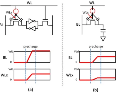
Fig. 5. Behavior of a transistor open fault on the pass transistor during a read operation for: (a) SRAM and (b) eDRAM.
power/ground shielding skills because the eDRAM is usually designed to be dense. Therefore, eDRAM is more sensitive to the coupling noise, such as word-line coupling and bit-line toggling, than SRAM. Consequently, for eDRAM testing, we need to focus more on the faults induced by coupling noise than that for SRAM testing.
3) Stuck-Open Fault: A major difference between SRAM and eDRAM in sensing is that the bit-line pair of most SRAM designs is precharged to Vdd for read operations while the bit-line pair of eDRAM is precharged to Vdd/2. The precharged-to-Vdd mechanism in SRAM’s read operations is used to prevent the data stored in the cross-coupled inverters from being attacked by the floating bit-lines, since the pass transistors in SRAM are all n-type MOSFETs and difficult to pull up the stored 0 value with a floating-1 bit-line. The precharged-to-Vdd/2 mechanism in eDRAM’s read operations is used to help its differential sensing, since only one-end of eDRAM’s bit-line pair is connected to the capacitor and per-form charge-sharing at the bit-line. Precharging the bit-lines to Vdd or Gnd will limit the differential sensing in one direction for eDRAM.
Due to the difference of their precharge mechanisms, the im-pact of the stuck-open fault occurring on a pass transistor is ferent for SRAM and eDRAM as well. Fig. 5 illustrates this dif-ference. When the stuck-open fault occurs on the pass transistor, it will introduce a floating node (WLx) at the gate of the pass transistor. The voltage of WLx will depend on the intrinsic cou-pling capacitor between the pass transistor’s gate and the bit-line (BL). If BL is precharged to Vdd like SRAM, the voltage of WLx will be raised to roughly the middle of Vdd and hence the pass gate will be half turn-on as shown in Fig. 5(a). If BL is precharged to Vdd/2 like eDRAM, the voltage of WLx will not be raised too much (more close to Gnd) and hence the pass gate can be reviewed as turn-off as shown in Fig. 5(b). As a result, the behavior of a transistor open fault is completely different between SRAM and eDRAM.
III. EDRAM TESTAPPROACH
A. Current SRAM Test Approach
In this section, we use the March C- algorithm as the basic skeleton of our eDRAM-testing algorithm. March C- algorithm is currently the most widely used test algorithm for SRAM in in-dustry, which can detect stuck-at faults (SAFs), transition faults (TFs), address decoder faults (AFs), inversion coupling faults (CFins), idempotent coupling faults (CFids), and state coupling faults (CFst) [1]. The following shows the element sequence of the March C- algorithm. The complexity of the March C- algo-rithm is 10 , where is the density of the array.
March C- (10N):
The notations are defined as follows. address direction do not care; address increase;
address decrease; data background;
complement data background; read;
write.
B. e-DRAM Test Strategies
Even though the interface of our eDRAM is the same as that of SRAM, applying only the SRAM test algorithm for eDRAM testing is not sufficient. Therefore, on top of this March C-algorithm, we need to add more elements to cover the faults which may not be considered in current SRAM testing but should be considered in the eDRAM testing, such as data-reten-tion faults, word-line coupling faults, bit-line toggling faults, and stuck-open faults. We also need to test the functionality which eDRAM has but SRAM does not, such as auto-refresh and self-refresh. In the following subsections, we provide the corresponding test strategy for each of the above uncovered faults and functions in the March C- algorithm.
1) Auto-Refresh and Self-Refresh: Auto-fresh and self-re-fresh are two functionalities which eDRAM has but SRAM does not. When the auto-refresh is activated, all eDRAM cells are re-freshed after every period of retention-time specification. When the self-refresh is activated, all eDRAM cells are refreshed and the retention-time counter for auto-refresh is reset. Therefore, in the eDRAM testing, the auto-refresh must be always on since the beginning and a self-refresh operation must be performed right before a “ra” element and a “rb” element individually to check the correctness of refreshing both “0” and “1”.
2) Retention Faults: The retention faults are caused by the cells which can not hold their charge for the specification-de-fined retention time. To test retention faults, we need to perform a self-refresh followed by a delay element, which will delay the next operation for the specification-defined retention time. At
the same time that the self-refresh is performed, the counter of the auto-refresh is reset. So after the delay element ends, the data will be auto-refreshed again. Then a read operation is per-formed to check if any retention fault occurs during the delay el-ement. During this retention test, the checkerboard background should be applied because this background can exacerbate the leakage and help to catch a retention fault. Note that the checker-board background here refers to data’s physical values, not log-ical values. Also, we need to perform this retention test to both the data-background and its complement.
3) Word-Line-Coupling Faults: In modern SRAM designs, the power/ground shielding technique is used to eliminate the signal disturbance between word-lines or bit-lines, and hence we seldom consider the word-line-coupling faults in SRAM testing. However, for eDRAM design, such technique cannot be applied due to its high-density requirement. In addition, the capacitive loading of a word-line in eDRAM is relatively large because more words are connected to a word-line in eDRAM than in SRAM. Word-lines are made of polysilicon that has much higher resistance than metal line. When a word-line is turned off too slowly due to its large RC delay, the voltage of the neighboring word-line might couple capacitively a voltage to the original word-line, resulting in a wrong state on the orig-inal word-line. In this case, a wrong data would be read from or write into the cells if a cell’s data on the original word-line is different from that of its adjacent word-line, such a scenario is easier to happen and test by the checkerboard background. Therefore, to detect word-line-coupling faults, a -direction MATS algorithm with a checkerboard background may be uti-lized. The sequence of a MATS algorithm is shown as follows. Its complexity is 4N.
MATS (4N):
Note that the -direction sequence refers to the physical word-line sequence, not the logical address sequence. For example in Fig. 4, the physical word-line sequence is “WL 0, 2, 1, 3, 4, 6, 5, 7”, not “WL 0, 1, 2, 3, 4, 5, 6, 7”. This address scrambling in -direction needs to be considered in the BIST circuitry.
4) Bit-Line-Toggling Faults: Testing SRAM needs not con-sider the bit-line toggling because of its power/ground shielding mechanism. A bit-line-toggling fault occurs when the bit-line or bit-line-bar of a cell is close to the bit-line or bit-line-bar of its adjacent cell, and these two adjacent lines have oppo-site data values. Because of higher density, one cell’s bit-line or bit-line-bar is closer to its adjacent cell’s bit-line or bit-line-bar than that in SRAM, eDRAM has higher probably of bit-line toggling fault. In order to create this scenario for each pair of adjacent cells, we need to perform the solid data-background because of the array scrambling as shown in Fig. 4. There-fore, the testing algorithm for eDRAM testing needs to cover bit-line-toggling faults, meaning that the proposed algorithm have to apply the solid data-background.
5) Stuck-Open Faults (SOFs): SOF occurs when the resis-tance between bit-line and switch transistor, switch transistor
and storage capacitor, or storage capacitor and ground is large. In this case, the data is hard to write into or read out from cells. Modern SRAM designs do not have this problem but some eDRAM cores do. SOFs can be detected at the same time as SAFs are detected when the sense amplifier is transparent to stuck-open faults. It means that the second element in March C- algorithm, (ra, wb), can already detect the SOFs in this case. When the sense amplifier is latch-based and thus not transparent to stuck-open faults due to the presence of the data latch, the test algorithm requires an element of (read, write, read) to detect the SOFs [1]. Therefore, we change the second element in March C- algorithm from (ra, wb) to (ra, wb, rb), which becomes the extended March C- algorithm.
C. Proposed Embedded-DRAM Test Approach
In this section, we summarize the test strategies discussed in Section III-B to form the final test approach for an eDRAM core. This test approach applies an -direction extended March C- algorithm with solid data-background as well as a -di-rection MATS algorithm with checkerboard data-background. Also, we test the self-refresh operation in the extended March C-algorithm and the retention faults in the MATS C-algorithm. The auto-refresh is always on in both algorithms. The detail steps of the March C- and MATS algorithms are described as follows.
-direction Extended March C- with solid background: EMC-:
;
(SR); .
-direction MATS with checkerboard background:
MATS: .
SR self-refresh;
del delay element which stops for the period of the retention time defined in the specification.
The test time (in terms of cycles) of the above EMC- and MATS algorithms are listed in (1) and (2)
(1) (2) where
total number of words; retention time; test frequency.
Note that, in the above equations, the number of cycles spent on self-refresh is since the 64 words at the same word-line will be refreshed at the same time. Also, the number of
cycles spent on one delay element is the specified retention time
times the frequency .
The above -direction extended March C- algorithm covers the stuck-open faults by the element (ra, wb, rb). It also tests the functionality of self-refresh and auto-refresh. The above -di-rection MATS algorithm tests the word-line-coupling faults by the -direction elements and checkerboard data-background. It also tests the retention faults by inserting the sequence of SR and del twice. The bit-line-toggling faults are covered by the solid-background operations in the extended March C- algorithm.
From coverage’s point of view, the two self-refresh opera-tions in the extended March C- algorithm seem redundant since two self-refresh operations are also performed in the MATS al-gorithm for the retention test. However, we keep the first two self-refresh operations in our first tape-out to differentiate the detection of self-retention faults from that of the data-retention faults. These two self-refresh operations in the extended March C- algorithm can be further removed to speed up the test time if the diagnosis requirement is low.
D. Experimental Results With ECC-On
In this subsection, we will perform different test approaches to the same eDRAM cores with the ECC circuitry turning on and without the retention tests, then compare the yield of each test approach. The test patterns are applied through external testers, not BIST circuitry. The reported results are collected from 1-lot wafers for this experiment. Following are the three test approaches to be applied individually:
1) the proposed test approach;
2) -direction March C- with solid background plus -di-rection MATS with CHK background;
3) -direction March C+ with solid background plus -di-rection MATS with CHK background.
The detail of March C+ (14N) is as follows:
The difference between proposed approach and the others is on their March algorithms in use. Approach 2 uses the basic March algorithm described in Section III-A and approach 3 uses the default March algorithm generated by a commercial memory-BIST tool, Memory BIST Architecture [23]. Note that we turn off the retention test in this experiment to save its test time. The experimental results containing the retention test will be discussed later in the Section IV.
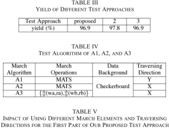
Table III lists the yield of the above three test approaches. Our proposed approach and Approach 3 result in the same yield while the Approach 2 results in a higher yield. This result im-plies that only applying March C- may miss certain faults and lead to higher test escape. The proposed approach can achieve the same level of fault coverage with Approach 3. However, the proposed approach only requires a 11N extended March C- al-gorithm but Approach 3 requires a 14N March C algorithm. This result shows that the general SRAM algorithm, March C-(10N), cannot provide sufficient fault coverage, and the default
TABLE III
YIELD OFDIFFERENTTESTAPPROACHES
TABLE IV
TESTALGORITHM OFA1, A2,ANDA3
TABLE V
IMPACT OFUSINGDIFFERENTMARCHELEMENTS ANDTRAVERSING
DIRECTIONS FOR THEFIRSTPART OFOURPROPOSEDTESTAPPROACH
March algorithm generated by a commercial tool, March C (14N), is redundant in our eDRAM testing.
E. Experimental Results With ECC-Off
In this subsection, we would like to share some internal exper-imental results which helped us to design the march elements, traversing direction, and data background used in our proposed test approach during the development stage. Those experiments are conducted by applying several similar march algorithms to the same eDRAM macros and comparing their resulting yields. Note that all the experiments in this section are performed with the ECC circuitry turning off, such that the impact of the de-tected defects will not be masked by the ECC circuitry and the yield difference between those test approaches can be more sig-nificant. Also, all the experiments in this subsection are con-ducted based on a different lot of wafers as used in Section III-D. Besides, all reported yields are represented as the difference to a base yield due to the confidential issue.
Table IV lists the march elements, data background, and traversing direction of three 4N march algorithms, denoted as A1, A2, and A3. As Table IV shows, A1 is the -direction MATS algorithm with checkerboard background, which is ac-tually the same algorithm used in the first part of our proposed test approach in Section III-C. Similar to A1, A2 is also a MATS algorithm with checkerboard background but traverses in the -direction. A3 is another 4N algorithm, performing a read operation right after a write operation and traverses twice.
Table V shows the relative yield after applying each of A1, A2, and A3 with the same extended March C- (EMC-) algo-rithm of the second part of our proposed approach (as shown in Section III-C). Note that the retention test is turned off in this experiment as well. In Table V, we can first find that A1 plus EMC- can result in a lower yield and capture more detects than A2 plus EMC-, which demonstrates the effectiveness and ne-cessity of using a -direction MATS algorithm rather than an -direction one in our proposed test approach. Compared to an -direction MATS algorithm, the additional faults detected by a -direction MATS algorithm are the word-line coupling faults (as discussed in Section III-B3), which is the source of the 6.2% yield difference between A1 and A2. Next, we can
TABLE VI
TESTALGORITHM OFB1ANDB2
TABLE VII
IMPACT OFUSINGDIFFERENTBACKGROUND FOR THE
SECONDPART OFOURPROPOSEDTESTAPPROACH
TABLE VIII
TESTALGORITHM OFC1, C2,ANDC3
also find in Table V that A2 plus EMC- can capture more de-fects than A3 plus EMC-, which further demonstrates the ad-vantage of using a MATS algorithm rather than another simple 4N march algorithm.
Table VI lists the march elements, data background, and traversing direction of two EMC- algorithms, denoted as B1 and B2. As Table VI shows, B1 uses a solid background while B2 uses a checkerboard background. Both B1 and B2 traverse in -directional. Table VII reports the yield after applying each of B1 and B2 with the -direction, checkerboard-background MATS algorithm (A2) but without the retention test. The result shows that B1 can detect 0.7% more defective parts than B2. This result demonstrates the advantage of using a solid-back-ground EMC- algorithm rather than checkerboard-backsolid-back-ground one in our proposed test approach. The additional faults de-tected by the solid background are bit-line-toggling faults (as discussed in Section III-B3). Compared to the result shown in Table V, we can also find that the occurrence of bit-line-toggling faults is less frequent than the occurrence of word-line-coupling faults for this eDRAM macro.
In the following experiment, we attempt to observe the impact of applying the retention test and the byte-write test. Table VIII lists description of three different MATS algorithms, denoted as C1, C2, and C3. C1 is the -direction checkerboard-back-ground MATS algorithm and does not include the retention test (same as A2). C2 is C1 plus retention test. C3 is C1 with all its write operations performed by byte-write, i.e., writing a byte (8) of bit-cells at a time instead of a word (32). Table IX shows the relative yield after applying each of C1, C2, and C3 with the same extended March C- (EMC-) algorithm used for Table V. As Table V shows, adding the retention test can detect 5.6% more defective parts, which demonstrates the effectiveness and necessity of applying the retention test in eDRAM testing. As to the byte-write test, only 0.2% more defective parts are detected, but its test application time is much larger since only 8 bits are written at one write operation. In addition, the application of the manufactured eDRAM macro is usually known when designing the SoC, and not all eDRAM’s applications need the
function-TABLE IX
IMPACT OFAPPLYINGRETENTIONTEST ANDBYTE-WRITETEST
TABLE X
TESTTIMEDISTRIBUTION OF THEPROPOSEDTESTAPPROACH
ality of byte-write. Hence the byte-write test can be omitted based on the application.
F. Test Time Analysis for Proposed Test Approach
The total test time of the proposed test approach is the summation of the test time on retention test , read/write
operations , self-refresh , and auto-refresh
(3) where (4) (5) (6) (7) time of one (del) element;
cycle time; number of words;
number of reads and writes; number of word-lines; number of self-refreshes; number of total auto-refreshes.
is equal to the retention-time specification, and is equal to the runtime divide by the specified retention time.
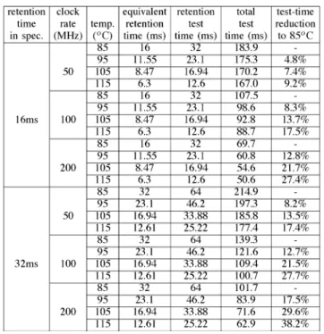
Table X lists the test time spent in each component of the proposed approach, given a 50 MHz clock frequency and a 16 ms retention-time specification. In this case, the ratio of reten-tion-test time to total test time is 17.4%.
We only assert auto-refresh signal when the run time of an element is longer than retention time. If the test clock is fast enough, the auto-refresh can be removed because elements are quickly done within retention time, but we still need one AR to verify the correctness of auto-refresh operation. The refresh can be done using a clock rate faster than test clock rate, here we still use the test clock rate to calculate refresh time.
In current eDRAM designs, the target clock frequency can be higher than the 50 MHz used in Table X. Table XI shows the ratio of the retention-test time to total eDRAM-test time for dif-ferent clock frequencies and difdif-ferent retention-time specifica-tions. As the results show, the ratio of the retention-test time in-creases when the clock frequency inin-creases, and gradually dom-inates the total eDRAM-test time. If the retention time is defined
TABLE XI
RATIO OFRETENTION-TESTTIME TOTOTALTESTTIME W.R.T. EACHRETENTION-TIMESPECIFICATION ANDCLOCKRATE
longer in the specification, this ratio would be even higher. For the case that clock frequency is 200 MHz and the defined re-tention time is 32 ms, this rere-tention-test-time ratio can be up to 62.9%. Therefore, reducing the retention-test time can signifi-cantly reduce the total eDRAM-test time. In Section IV, we will attempt to increase the temperature to further reduce the reten-tion-test time.
Another way to further reduce the total test time is to apply the burst mode operation, if the eDRAM core supports, for a single-operation March element, such as the (wa) and (ra) in the extended March C- algorithm. However, this reduction is still limited since most elements contain more than one operations.
IV. REDUCING RETENTION-TEST TIME BY INCREASINGTEMPERATURE
For an eDRAM cell, its data-retention time is determined by the leakage of its switch transistor, which increases along with the increase of the temperature. In the eDRAM testing, we at-tempt to raise the temperature to increase transistor’s leakage current, which shortens the data-retention time of a cell. There-fore, at a higher temperature, the delay element used for reten-tion test can be specified shorter since a retenreten-tion fault can be detected within a shorter period of time than that at the original reference temperature. However, if the new specified retention time is too low, some retention faults may be able to escape, re-sulting in a higher defect level. On the contrary, if it is too high, the retention time of an eDRAM cell is over-tested, resulting in a yield lost.
In order to specify an appropriate retention time for the delay element at a higher temperature, we need to calculate the time at a given temperature during that the leakage of a switch transistor is equivalent to the leakage during the specified retention time at the reference temperature, which is defined as 85 C in our specification. This time is defined as the equivalent retention time for a given temperature, which implies that a eDRAM cell loses its data after the specified retention time at 85 C if and only if this cell will lose its data after the equivalent retention time at the given temperature.
In the following of this section, we first study different leakage mechanisms of a switch transistor and their sensitivity to the temperature. Based on this leakage analysis, we then calculate the equivalent retention time. Last, the experimental results of using different equivalent retention time at different temperatures are presented. We will also compare the total test-time reduction by increasing the temperature.
Fig. 6. Main leakage sources of a eDRAM cell.
A. Leakage Mechanisms
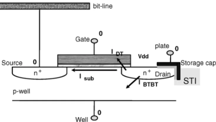
The leakage mechanisms of a deep-sub-micron transistor include reverse-bias pn junction leakage, subthreshold leakage, oxide tunneling current, gate current due to hot-carrier injection, gate-induced drain leakage (GIDL), and channel punchthrough current [17]. Among these six leakage mechanisms, the re-verse-bias junction band-to-band-tunneling (BTBT) leakage, subthreshold leakage, and direct tunneling current are the main leakage sources in current advanced process technologies [16]. Fig. 6 illustrates these three main leakage sources in the cross-section view of a cell in our eDRAM. The detail analysis for each of the above leakage sources and its relation to temperature are presented as follows.
1) Reverse-Bias Junction BTBT Leakage: Drain and source to well junctions are commonly reverse-biased for preventing forward-biased current. If both and region are heavily doped, band-to-band tunneling dominates the junction leakage. The BTBT current involves the emission or absorption of phonons, since silicon is an indirect band gap semiconductor. The tunneling current density is as follows [24]:
(8)
where , and
is the effective mass of electron; is the energy-band gap; is the applied reverse bias; is the electric field at the junction; is the electronic charge; and is the reduced Planck’s constant. The electric field at the junction is
(9)
where and are the doping in the and side,
respec-tively; is permittivity of silicon; is the built in voltage across the junction.
2) Subthreshold Leakage: Subthreshold leakage occurs when gate voltage is below . In the weak inversion, the diffusion current occurs in the subthreshold conduction when the minority carriers are conducted from channel region and exist in channel depletion layer. This subthreshold current can be expressed as follows [24]:
where
(11)
where is the threshold voltage; is the thermal
voltage, is temperature; is the gate-oxide capacitance; is the zero-bias mobility; is the subthreshold swing coefficient (also called body effect coefficient); is the maximum de-pletion-layer width; is the gate-oxide thickness.
3) Gate Tunneling Current: The high electric field coupled with low oxide thickness causes tunneling of electrons both from substrate to gate and from gate to substrate, resulting in the gate-oxide-tunneling current. The direct tunneling mechanism occurs in more advanced devices because the potential drop across the oxide is smaller than the barrier height of Si-SiO . The current density of direct tunneling can be expressed as fol-lows [24]:
(12)
where and
is the electric field across the oxide.
When a DRAM cell stores “1”, its bias condition is illustrated
in Fig. 6. and induce a subshreshold
cur-rent. means that drain-substrate is reverse-biased, which induces BTBT leakage. In addition, the direct tunneling current also may occur because the voltage across the intersec-tion of drain and gate is equal to . Hence, the total leakage current of the switch transistor for a given temperature
can be expressed as
(13) where and is the tunneling area of direct tunneling and BTBT.
Note that this leakage is actually a function of temperature. The following subsection discusses those temperature-depen-dent parameters in the above leakage equations. In addition, the leakage for the storage capacitor itself is small when using a high- material and hence can be omitted in our analysis. B. Temperature-Dependent Parameters in Leakage
Different leakage-current sources have different temperature dependence. In the following, we list the temperature-depen-dent parameters in above three leakage equations and discuss the magnitude of their dependency to the temperature .
1) Energy-Band Gap : The energy-band gap may be narrowed by the increase of temperature within an order of
.
2) Junction Electric Field : The junction electric field coupled with the doping concentration may be influenced by the temperature, but it is more dependent on the junction voltage.
3) Mobility : The increase of temperature results in the reduction of mobility. The degradation of mobility is direct pro-portional to .
4) Thermal Voltage : The thermal voltage is linearly pro-portional to the temperature, which results in an exponential growth of the subthreshold leakage.
5) Threshold Voltage : The increase of temperature causes more carriers on the channel, which reduces the threshold voltage and hence increases the subthreshold leakage.
6) Barrier Height : The barrier height decreases when temperature increases, which is proportional to .
In summary, the direct-tunneling current is invariant to the temperature since the barrier height and potential drop across oxide are invariant to the temperature. The BTBT leakage may vary with the temperature but only in a small order. The sub-threshold leakage increases significantly along with the increase of the temperature due to the decrease of and the increase of thermal voltage. Even though the direct-tunneling current and BTBT current are not sensitive to the temperature, both of them should still be considered in our leakage analysis since they con-tribute a significant portion of the total leakage at the normal temperature especially in advanced process technologies [16]. C. Analysis of Equivalent Retention Time
To calculate the equivalent retention time for a target tem-perature, we first calculate the total amount of charge
leaked from the storage capacitor during the retention-time
specification at the reference temperature , i.e.,
85 C. Then the leakage during the equivalent retention time at the target temperature has to be equivalent to , which is expressed in (14)
(14) Therefore, the equivalent retention time at the target temperature can be obtained by (15)
(15) The parameters used in the leakage calculation are listed as follows, which are provided by the IC foundry and may vary from the following different process technologies.
Mobility : – (m /V s). Oxide Capacitance : – (F/m ). Oxide Thickness : – (m). Channel Width : – (m). Channel Length : (m). Subthreshold Swing : 1.1–1.5. Thermal Voltage : (V). Threshold Voltage : 0.4–0.6 (V). Supply Voltage : 1.2 (V).
Barrier Height : 3.1–3.2 (eV).
Energy Band-gap :
(eV).
Doping Concentration: about (m ).
Table XII lists the calculated equivalent retention time and its reduction ratio to the original specification-defined retention time associated with each given temperature. The retention-time specification is 16 ms at the reference temperature 85 C. As the results shows, the retention-time reduction is close to 50% when raising the temperature to 105 C, and 65% when
TABLE XII
CALCULATEDEQUIVALENTRETENTIONTIME ANDITSREDUCTION TO THE
RETENTION-TIMESPECIFICATION16MS AT85 C
TABLE XIII
YIELD W.R.T.EACHTEMPERATURE ANDRETENTION-TIMESPECIFICATION
120 C, respectively. It implies that the retention-test time can be significantly reduced by raising the temperature.
D. Experimental Results
In the following experiment, we apply our proposed test algo-rithm (described in Section III) on the eDRAM cores of 1-lot test wafers repeatedly with different retention-time specifications at different temperatures. In each time of the eDRAM testing, the delay element needs to match the retention-time specifica-tion. Table XIII shows the corresponding yield for each reten-tion-time specification and temperature. As the results show, the yield reaches 86.5% with 16 ms retention time at 85 C. Also, the same yield is first-reached with 12 ms retention time at 95 C and 8 ms retention time at 105 C. This result implies that the eDRAM cells which hold their charge for 16 ms at 85 C can hold their charge for 12 ms at 95 C and for 8 ms at 105 C, respectively. This result approximately matches the calculated equivalent retention time listed in Table XII, where the equiva-lent retention time for 95 C and 105 C is 11.55 and 8.49 ms, respectively.
Note that we are not suggesting to directly use the calculated equivalent retention time during the eDRAM testing. The equiv-alent retention time used in practice should be verified through real silicon experiments. For the IC foundry providing eDRAM cores, a table of equivalent retention time associated with dif-ferent temperatures can be built through a similar experiment as shown in Table XIII. However, it may take weeks or even longer to build a complete yield table with respect to each tem-perature and each retention-time specification. The cost of re-peatedly testing the same wafers should be considered. This cost limitation is also the reason why the resolution of the retention time in Table XIII is in 2 ms, not in a smaller, more accurate unit of time. Therefore, our theoretical calculation of the equivalent retention time can be used as an efficient guideline during the above process of searching the equivalent retention time with silicon experiments, which can save the high cost of repeatedly testing a significant number of test wafers.
Table XIV further shows the total eDRAM-test-time reduc-tion which can be achieved by increasing the testing temper-ature. In Table XIV, Columns 4, 5, and 6 list the equivalent
TABLE XIV
TESTTIMEREDUCTION W.R.T. EACHRETENTION-TIMESPECIFICATION, CLOCKRATE,ANDTEMPERATURE
retention time, retention-test time, and total eDRAM-test time, respectively, associated with each retention-time specification at 85 C, clock frequency, and temperature. Column 7 list the total eDRAM-test-time reduction achieved by using the equiva-lent retention time at each temperature compared to the total test time at 85 C. As the results show, this total eDRAM-test-time reduction increases when the temperature, clock frequency, or retention-time specification increases. The reduction ratio can be up to 38.2% by increasing 30 C at temperature when the retention-time specification and clock frequency are 32 ms and 200 MHz, respectively.
Note that at a higher temperature, its equivalent retention time decreases, which results in more frequent auto-refresh opera-tions. Fortunately, the time consumed by a refresh operation is short and does not affect test-time reduction too much. In ad-dition, the temperature discussed here is for wafer testing. If we want to test the data retention after package, the tempera-ture under consideration should be the temperatempera-ture inside the package, not just tester’s temperature. The temperature inside the package is higher than that outside the package. The table to map package’s outside temperatures to its insides temperature can be obtained from the package providers.
Also, increasing the temperature at test may fail more dies than that at the normal temperature since the dies are literally tested under a condition similar to a burn-in test, which may also be a test item requested from the customers to detect the infant-mortality dies and further reduce the defect level. There-fore, increasing the temperature at test can cover two needs at the same time, one for reducing the retention test time and the other for improving the defect level. Besides, to elevate the oven’s temperature to the desired level may take extra time, which is another overhead of increasing temperature at test. For-tunately, as long as the temperature is increased to the desired
level, we can keep on sending the wafers into the oven and apply test continually. Thus, the overhead of increasing the oven’s temperature is a one-time overhead, whose impact can be fur-ther reduced if the volume of the order is large.
V. DEFECT-LEVELESTIMATION OFWEAR-OUTDEFECTS UNDERECC
Reliability testing, such as THB test [18], HAST test [19], and HTOL test [20], is applied to measure the reliability or lifetime of manufactured chips by operating them under an extreme con-dition of certain environmental or electrical parameters. Those extreme conditions can accelerate the wear-out failure mech-anisms, such as electron migration, dielectric breakdown, hot carrier effects, and mobile ionic contamination. Hence we could use the result of the above reliability testings to foresee the product’s failure rate occurring after certain months or years of usage. This failure caused by the wear-out defects is one source of product’s defect level.
In current industry, the cost of the above reliability testings is still expense. Also, the application time of a reliability testing may take several days or sometimes even weeks (such as THB test). As a result, unlike the production burn-in testing, which is applied to each part to accelerate the infant-mortality failures, a reliability testing can only be applied to a small portion of the products to accelerate the wear-out failures. Thus, in this section, we provide a mathematical model to estimate the defect level of a eDRAM macro resulting from the wear-out defects based on limited samples. Also, this model considers the use of ECC circuitry, which is seldom used in commodity DRAMs, especially MCM DRAM KGDs.
The most straightforward method to estimate this defect level is just to run the reliability testing with the ECC function and count the failed parts at the end. However, the number of sampled parts for the reliability testing is usually around few hundreds and the general acceptable defect level is under 100 DPPM. This sampling size is not enough to support such a fine resolution of the defect level. For example, in our own THB or HTOL test of an eDRAM product, we sample total 231 parts (77 parts per lot for three consecutive lots) and our target defect level is 32 DPPM. Therefore, instead of counting the failed parts, we directly count the number of defective eDRAM cells for each part before and after the reliability testing. Because the ECC circuitry may mask the effect of some defective cells, we need to turn off the ECC function and directly read the data from cells, which requires a bypass mode of the ECC circuitry to realize this action. As described above, we can obtain the probability distribution of the number of the added defective cells on a part during the reliability testing.
Those defective cells resulting from the wear-out defects are actually random single defects, and thus the above probability distribution can be modeled by the Poisson distribution. The re-sult of our internal experiment also confirms this Poisson distri-bution. The most important parameter for a Poisson distribution is its , which represents the mean of the Poisson distribution. Based on few hundreds of sampled parts, the sampled mean of the number of added defective cells after the reliability testing is more reliable than the sampled DPPM. To estimate the defect
Fig. 7. Relations among , and
.
level under ECC, we also need to obtain the probability distri-bution of the number of single defects existing before applying the production testing, which is a Poisson distribution as well and can be collected from the production testing.
Before introducing our mathematical model of estimating this defect level with the use of ECC, we first define the following notations:
• : the number of bits per word;
• : the number of words in one memory chip;
• : the number of bits in one memory chip ;
• : the random variable denoting the number of single defects existing before applying the production testing; • : the mean of the random variable ;
• : the random variable denoting the number of added single defects during the reliability testing;
• : the mean of the random variable ; • : the probability that event occurs;
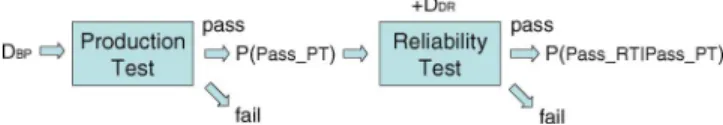
• : the event that a part containing random single defects passes the production testing with the use of ECC; • : the event that a part containing random single defects passes the reliability testing with the use of ECC; • DL: the defect level caused by the wear-out defects. The defect level caused by the wear-out defects is equal to
, where
represents the probability that a part passes the reliability testing in condition that the part passes the production testing. Fig. 7 illustrates the relations among
, and .
Once the part passes the reliability testing, it must be able to pass the production testing. Hence, we can calculate the defect level, DL, by the following equation:
(16) When applying the production testing, the number of defects in a part is . To pass the production test, there cannot exist two defects in a word given the . Thus, the
is equal to
(17) where represents the possible combinations that the defects locate in different words and represents the total possible combinations that defects locate in the memory array.
means the probability that a part passes the relia-bility testing regardless it passes the production testing or not. Thus, when applying the reliability testing, the number of
de-fects in a part should be . Both and are
Poisson distributions and hence the convolution of and is also a Poisson distribution, whose is equal to .
Thus, is equal to
(18) With (16), (17), and (18), the defect level DL with the use of ECC can be obtained. Note that the above equations consider only the random single defects and omit the impact of the row, column, and clustered defects. This is because the ECC used in current memory designs can only tolerate one error per word. As long as any of the row, column or clustered defects occurs, the part usually fails the production testing already and hence needs not be considered here. Therefore, the
in this section does not mean the yield after the production
testing. only considers the impact of random
single defects.
VI. CONCLUSION
The eDRAM testing mixes up the techniques of SRAM testing and commodity-DRAM testing since eDRAMs use the SRAM interface and DRAM cells. In this paper, we first introduced an exemplary eDRAM design and discussed the key issues which should be emphasized in eDRAM testing by comparing to commodity-DRAM testing and SRAM testing. Then we started from a short SRAM algorithm and discussed the fault models that are not covered by the SRAM testing but should be considered in eDRAM testing. We also discussed the impact of those faults and how to design a test algorithm to detect them. Furthermore, we analyze the relation between switch transistor’s leakage and temperature. Based on that, we can theoretically calculate the equivalent retention time for different temperatures which can be adopted to reduce the retention-test time. Last, we proposed a mathematical model to estimate the defect level caused by wear-out defects under ECC, which is a special function used in eDRAM compared to the commodity-DRAMs.
REFERENCES
[1] A. J. van de Goor, Testing Semiconductor Memories, Theory and
Prac-tice. Gouda, The Netherlands: ComTex, 1998.
[2] G. Wang, K. Cheng, H. Ho, J. Faltermeier, W. Kong, H. Kim, J. Cai, C. Tanner, K. McStay, K. Balasubramanyam, C. Pei, L. Ninomiya, X. Li, K. Winstel, D. Dobuzinsky, M. Naeem, R. Zhang, R. Deschner, M. J. Brodsky, S. Allen, J. Yates, Y. Feng, P. Marchetti, C. Norris, D. Casarotto, J. Benedict, A. Kniffm, D. Parise, B. Khan, J. Barth, P. Parries, T. Kirihata, J. Norum, and S. S. Iyer, “A 0.127 m high per-formance 65 nm SOI based embedded DRAM for on-processor appli-cations,” in Proc. Int. Electron Devices Meet., 2006, pp. 1–4. [3] E. Gerritsen, N. Emonetb, C. Caillatb, N. Jourdanb, M. Piazzab, D.
Frabouletd, B. Boeckc, A. Berthelota, S. Smitha, and P. Mazoyerb, “Evolution of materials technology for stacked-capacitors in 65 nm em-bedded-DRAM,” Solid-State Electron., vol. 14, pp. 1767–1775, 2005.
[4] M.-E. Jones, “1T-SRAM-Q™: Quad-density technology reins in spi-raling memory requirements,” Mosys, Inc., Santa Clara, CA, 2007. [5] A. Berthelot, C. Caillat, V. Huard, S. Barnola, B. Boeck, H. Del-Puppo,
N. Emonet, and F. Lalanne, “Highly reliable TiN/ZrO /TiN 3D stacked capacitors for 45 nm embedded DRAM technologies,” in Proc.
Solid-State Device Res. Conf., 2006, pp. 343–346.
[6] TSMC, Hsinchu, Taiwan, “TSMC embedded high density memory,” [Online]. Available: http://www.tsmc.com/
[7] UMC, Hsinchu, Taiwan, “0.13 micron SoC process technology,” [On-line]. Available: http://www.umc.com/
[8] M.-R. Amerian, W. D. Atwell, I. Burgess, G. D. Fleeman, D. Y. Lepe-jian, T. W. Williams, F. Zarrinfar, and Y. Zorian, “A D&T Roundtable: Testing mixed logic and DRAM chips,” IEEE Design Test Comput., vol. 15, no. 2, pp. 86–92, Apr.–Jun. 1998.
[9] C. Cheng, C.-T. Huang, J.-R. Huang, C.-W. Wu, C.-J. Wey, and M.-C. Tsai, “BRAINS: A BIST compiler for embedded memories,” in Proc.
IEEE Int. Symp. Defect Fault Toler. VLSI Syst., 2000, pp. 299–307.
[10] J.-F. Li, R.-S. Tzeng, and C.-W. Wu, “Diagnostic data compression techniques for embedded memories with built-in self-test,” J. Electron.
Test.: Theory Appl., vol. 18, no. 4, pp. 515–527, Aug. 2002.
[11] B. Nadeau-Dostie, A. Silburt, and V. K. Agarwal, “Serial interfacing for embedded memory testing,” IEEE Design Test Comput., vol. 7, no. 2, pp. 52–63, Apr. 1990.
[12] C.-T. Huang, J.-R. Huang, C.-F. Wu, C.-W. Wu, and T.-Y. Chang, “A programmable BIST core for embedded DRAM,” IEEE Design Test
Comput., vol. 16, no. 1, pp. 59–70, Jan.–Mar. 1999.
[13] J. E. Barth, J. H. Dreibelbis, E. A. Nelson, D. L. Anand, G. Pomichter, P. Jakobsen, M. R. Nelms, J. Leach, and G. M. Belansek, “Embedded DRAM design and architecture for the IBM 0.11- m ASIC offering,”
IBM J. Res. Develop., vol. 46, no. 6, pp. 675–689, Nov. 2002.
[14] S. Miyano, K. Sato, and K. Numata, “Universal test interface for em-bedded-DRAM testing,” IEEE Design Test Comput., vol. 16, no. 1, pp. 59–70, Jan.–Mar. 1999.
[15] N. Watanabe, F. Morishita, Y. Taito, A. Yamazaki, T. Tanizaki, K. Dosaka, Y. Morooka, F. Igaue, K. Furue, Y. Nagura, T. Komoike, T. Morihara, A. Hachisuka, K. Arimoto, and H. Ozaki, “An embedded DRAM hybrid macro with auto signal management and enhanced-on-chip tester,” in Dig. Tech. Papers IEEE Int. Solid-State Circuits Conf.
(ISSCC), 2001, pp. 388–389.
[16] S. Mukhopadhyay, A. Raychowdhury, and K. Roy, “Accurate estima-tion of total leakage in nanometer-scale bulk CMOS circuits based on device geometry and doping profile,” IEEE Trans. Comput.-Aided
De-sign Integr. Circuits Syst., vol. 24, no. 3, pp. 363–381, Mar. 2005.
[17] K. Roy, S. Mukhopadhyay, and H. Mahmoodi-Meimand, “Leakage current mechanisms and leakage reduction techniques in deep-submi-crometer CMOS circuits,” Proc. IEEE, vol. 91, no. 2, pp. 305–327, Feb. 2003.
[18] Electronic Industries Association and JEDEC Solid State Technology Association, Arlington, VA, “Steady state temperature humidity bias life test,” EIA/JESD22-A101-B, Apr. 1997.
[19] Electronic Industries Association and JEDEC Solid State Technology Association, Arlington, VA, “Highly-accelerated temperature and hu-midity stress test,” EIA/JESD22-A110-B, Jun. 2008.
[20] JEDEC Solid State Technology Association, Arlington, VA, “Temper-ature, bias, and operating life,” JESD22-A108C, June 2005. [21] A. J. van de Goor and I. Schanstra, “Address and data scrambling:
Causes and impact on memory tests,” in Proc. 1st IEEE Int. Workshop
Electron. Design, Test, Appl., 2002, pp. 128–136.
[22] K.-L. Cheng, M.-F. Tsai, and C.-W. Wu, “Neighborhood pattern-sensi-tive fault testing and diagnostics for random-access memories,” IEEE
Trans. Comput.-Aided Design Integr. Circuits Syst., vol. 21, no. 11, pp.
1328–1336, Nov. 2002.
[23] Mentor Graphics Corporation, Wilsonville, OR, “MBIST architecht reference manual,” Vol. 8, Mar. 2003.
[24] Y. Taur and T. H. Ning, Fundamentals of Modern VLSI Devices. New York: Cambridge Univ. Press, 1998.
[25] A. Pavlov, M. Azimane, J. P. de Gyvez, and M. Sachdev, “Word line pulsing technique for stability fault detection in SRAM cells,” in Proc.
IEEE Int. Test Conf., 2005, pp. 816–825.
[26] L. Dilillo, P. Girard, S. Pravossoudovitch, A. Virazel, and H. H. Magali Bastian, “Data retention fault in SRAM memories: Analysis and detec-tion procedures,” in Proc. IEEE VLSI Test Symp., 2005, pp. 183–188. [27] J. Yang, B. Wang, Y. Wu, and A. Ivanov, “Fast detection of data
reten-tion faults and other SRAM cell open defects,” IEEE Trans.
Comput.-Aided Design Integr. Circuits Syst., vol. 25, no. 1, pp. 167–180, Jan.
[28] A. Ney, L. Dilillo, P. Girard, S. Pravossoudovitch, A. Virazel, M. Bas-tian, and V. Gouin, “A new design-for-test technique for SRAM core-cell stability faults,” in Proc. Design, Autom., Test Eur. Conf. Exhib., 2009, pp. 1344–1348.
[29] L. Dilillo, P. Girard, S. Pravossoudovitch, A. Virazel, S. Borri, and H. H. Magali, “Resistive-open defects in embedded-SRAM core cells: Analysis and march test solution,” in Proc. Asian Test Symp., 2004, pp. 266–271.
[30] Q. Chen, H. Mahmoodi, S. Bhunia, and K. Roy, “Efficient testing of SRAM with optimized march sequences and a novel DFT technique for emerging failures due to process variations,” IEEE Trans. Very Large
Scale Integr. Syst., vol. 13, no. 11, pp. 1286–1295, Nov. 2005.
Hao-Yu Yang received the B.S. degree from the Electrical Engineering and Computer Science Un-dergraduate Honors Program at National Chiao Tung University, Hsinchu, Taiwan, in 2009. He is currently pursuing the Ph.D. degree in electronics engineering from the Institute of Electronics, National Chiao Tung University, Hsinchu, Taiwan.
His current research interest is memory testing.
Chi-Min Chang received the B.S. degree from the Department of Electrical Engineering, National Cen-tral University, Taoyuan, Taiwan, in 2006, and the M.S. degree from the Department of Electronics En-gineering, National Chiao Tung University, Hsinchu, Taiwan, in 2008.
He is with Taiwan Semiconductor Manufacturing Company, where he focused on test structure de-signing and WAT testing.
Mango C.-T. Chao received the B.S. and M.S. degrees from the Department of Computer and In-formation Science, National Chiao Tung University, Hsinchu, Taiwan, in 1998 and 2000, respectively, and the Ph.D. degree from the Department of Electrical and Computer Engineering, University of California, Santa Barbara, in 2006.
He is an Assistant Professor with the Department of Electronics Engineering, National Chiao Tung University. His current research interests include VLSI testing, TFT circuitry design, and physical design automation.
Rei-Fu Huang received the B.S. and Ph.D. degrees from the Department of Electrical Engineering, National Tsing Hua University, Hsinchu, Taiwan. He is a technical Manager with MediaTek Inc., Hsinchu City, Taiwan. His research interests include memory intellectual property design and testing.
Shih-Chin Lin received the B.S. and M.S. degrees from the Department of Electrical Engineering, Na-tional Chiao Tung University, Hsinchu, Taiwan.
He is a director with UMC IP Design Division, Hsinchu City, Taiwan. His research interests include memory intellectual property design and testing.