each of the images and the distance to the object. In the system described, an effective separation of the optical paths of -6” is obtained by selective use of part of the area of the single objective lens for left and right images. In the case of a typical endoscope view with objects some 30 to l00mm from the objective lens, this 6mm separation, when compared to a normal interoccular distance of 60mm, gives a similar perceived depth as objects at -30cm to lm .
l a v e r substrate reference electrode
left right
upper substrate electrodes ~ Fig. 3 Electrode pattevn for ferroelectric LCD
axis
Evalution and discussion: The image quality obtained using the FELC device with the 740 line CCD camera was excellent, the introduction of the liquid crystal device produced no noticeable degradation of the image. The necessary use of polarisers on the electro-optic device incurs a light loss of -50% in addition to the light lost due to obscuring part
of
the optical path. This is the most serious limitation and further work is planned to investigate the trade-off between contrast ratio and stereoscopic separation.The FELC device proved ideal for this application, as the drive signal for the shutter elements were easily derived from the camera and framestore circuits. To switch the FELC device, a charge of -35nC must be supplied to the device during the switching period of 50 p. This gives a modest drive requirement of < 1 nA . These requirements were easily met; the two elements of the LC shutter were driven in antiphase from a signal derived from the image capture cycle of the CCD camera and framestore.
In the absence of objective evaluation procedures for stereoen- doscopes, subjective initial trials were carried out with a number of different operators, and a wide variety of objects in the endo- scope field of view. The camera system using the FELC shutter was compared with a system using a beamsplitter fitted with two cameras and also with an Olympus twin channel endoscope. The present system showed a signifcant advantage in terms of image brightness over the Olympus endoscope and gave a better per- ceived stereo image. The image and stereoscopic quality was judged to be as good
as
that using the beam splitter and dual cam- era system, but use of the FELC shutter allows the system to be less bulky and only half of the weight. To allow more accurate comparison between systems, standard tests are under develop- ment, the results of which will be reported in a later paper.The endoscope
camera
system presented here useda monitor and shutter glasses. This arrangement has the advantage over VR types of display in that it does not obscure the surroundings. In the future, the output from the camera described here may be dis- played using one of the ‘glasses free’ viewing systems currently under development [5].Conclusions: A stereoscopic image capture system for use with an endoscope has been described. The use of ferroelectric liquid crys- tal electro-optic devices to modify the optical path at video rates, both for the camera and the l00Hz frame rate viewing system, has been successfully demonstrated. The stereo separation achieved is limited by the physical dimensions of the endoscope and the con- trast ratio of the FELC device. The electro-optic switching speed and contrast of this device have been shown to be capable of
giving good image separation and depth perception. The loss of image quality due to the insertion of the FELC device in the opti- cal path has proved to be negligible with the camera in use. The ability to capture and display stereoscopic images has other appli- cations; it could be used for enhancing the effectiveness of inspec- tion procedures with a variety of instruments.
Acknowledgments: Thanks are due to B. Hodder and R. Sambles of Exeter University Physics Department for assistance in the manufacture of the LC devices used in this work. We also thank M. Lewis of GMMT for materials used in the LC device. 0 1EE 1991
Electronics Letters Online No: 19970582
G.A. Lester (School of Engineeving, University of Exeter, Exeter EX4
4QF, United Kingdom)
J. Watts (Liquid Vision Ltd., Old Workshops, Farvingdon, Exetev, EX5 2 JD, United Kingdom)
D. Wilmington (Mantracourt Electronics Ltd., Furringdon Park, Exeter EX5 ZJB, United Kingdom)
20 March 1997
References
DURRANI, A.F., and PREMINGER, G.M.: ‘Three-dimensional video
imaging for endoscopic surgery’, Cumput. Biol. Med., 1995, 25, pp.
MITCHELL, T . N , ROBERTSON, J., NAGY, A.G., and LOMAX, A.: ‘Three-
dimensional endoscopic imaging for minimal access surgery’, J. R. Coll. Surg. Edin., 1993, 38, pp. 285-292
STAVA, R.M : ‘3-D vision technology applied to advanced minimally invasive surgery systems’, Surg. Endoscopy, 1993, 7, pp. 429431
LESTER, G.A., COLES, H., MURAYAMA, A , and ISHIKAWA, M.: ‘Electro-
optic behaviour of low molar mass FELCs doped with liquid crystal polymers’, Ferroelectrics, 1993, 148, pp. 389-399
VAN BERKEL, c., FRANKLIN, A R
,
and MANSELL, J.R.: ‘Design andapplications of multiview 3D-LCD’. Proc. 16th Int. Conf. Dsiplay Research, Birmingham, 1996, pp. 109-1 12
237-241
Highly accurate cyclic
CMOS
time-to-digital
converter with extremely low power
consumption
Poki
Chen,
Shen-Iuan Liu and
JingshownWu
Indexing terms: CMOS integrated circuits, Instrumentation The authors propose a new cyclic structure for a CMOS time-to- digital converter (TDC). The measured single-shot resolution is 286ps, and the measured single-shot accuracy is C. 143ps. The new circuit can be shut down be.tween measurements which makes the circuit suitable for portable applications.
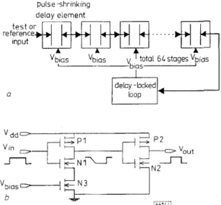
Introduction: Time interval digitisation is
an
important element for many instrumentation circuits, such as range finders and the phasemeters El], etc. Owing to large power consumption, conven- tional TDCs with subnanosecond resolution cannot easily be real- ised in portable systems. Recently, a novel TDC circuit, as shownin
Fig.la, was
proposedto obtain
780ps resolution (after averag- ing hundreds of measurements) with only 15mW power consump- tion [2]. The price is 3ns single-shot accuracy.The degree of pulse shrinking of the delay element, in Fig. lb, is controlled by V,,, [2]. For calibration, a stabilised reference period
Tef
is fed into a delay line. The delay-locked loop will adjust V,, to makeTF,
reduce to zero exactly at the end, stage N , of the delay line. When a measurement is requested, the input period T,,will be fed through instead. Suppose that
r,,
reduces to zero at the nth stage, its width is then measured asn
x TJN.This circuit was a significant advance for low-cost, high-accu- racy portable TDC systems. However, some important features still need to be improved. First, the delay line must be folded into segments, due to reasonable chip width or length limits. The inter- segment wiring is much longer than that for intra-segment wiring,
and causes a large linearity error [3]. Secondly, the mismatch among delay elements results in poor TDC linearity. Thirdly, the pulses reduce in width more rapidly at the last few stages, because they become too short to drive the next stage to toggle its state. Next, the calibration, which must be carried out continuously to make i".cl reduce exactly to zero at the last stage, consumes too much power [2, 31. Finally, this TDC must double the size of i1.s delay lines to only increase one output bit. To overcome thesie problems,
a
new TDC with a cyclic delay line is proposed.p u k e -5hrinkl'ng delay element -b A A Vbias vbias t e s t o r input reference+ . . . I r--J--7 I a
n
'biasD-{ N 3 bFig. 1 Block diagram of original CMOS TDC and pulse-shrinkin>: delay element
a Block diagram of' original CMOS TDC b Pulse-shrinking delay element used in Fig. l a
Circuit description: As shown in Fig. 2a, the input pulse circulates in the proposed cyclic delay line. It reduces in width slightly each cycle until thoroughly diminished. Assume that the counter counts
N for Trd and n for T,?,. T,,, is then measured as n x T,,IN theoreti- cally. For practical implementation, the delay line is replaced by series-connected pulse-shrinking delay elements (Fig. 2b). We ca:n adjust V,,,, to make
r.,
circulate over hundreds or thousands c'f cycles to obtain extremely fine resolution.pulse -shrinking delay element
delay line counter
a
testor reference output p u k e b
Fig. 2 Conceptual block diagram of new T D C and sealisation of cyclic TDC in Fig. 2a
a Conceptual block diagram of new TDC
b Realisation circuit of cyclic TDC in Fig. 2a
The input pulse will go through the whole delay line once per cycle. The element mismatch and intra-segment wiring mismatch discussed will not cause any measurement nonlinearity from cycle to cycle. It is unnecessary to make just disappear at some spe- cific cycle or stage. Sufficient resolution is obtained only if Vhii,\ is properly adjusted so that
ref
circulates through the delay line iisufficient number of times before it vanishes. A slight variation in the output count N for T,,i is tolerable and continuous calibration is no longer needed. The circuit can not only be greatly simplified, but can also be shut down between measurements to save power.
The number of output bits of the new TDC is unlimited and can be increased by merely lengthening the internal counter in Fig. 2b, and control of
!&,,
made finer correspondingly. No averagingis needed to improve the resolution, because the single-shot resolu- tion is accurate enough. The nonlinearity, caused by the pulse reducing in width more rapidly at the last few stages, can be treated as a constant count offset for a given V,,,,. It can be com- pletely calibrated out by the following technique. First, i'+ and 7;.,,/2 are fed into the TDC input and we assume that the circuit obtains Nand N' counts, respectively. We have
T T e f =
+
T o f f s e twhere a = effective resolution
T,,f
2 = aN'+
T o f f s e t (1)Then, T,,z is fed into the TDC input, and the output count is assumed to be I. After solving
a
and T,,,, from eqn. 1, we obtainTcr
and T,d2 must be re-measured for each7;,
measurement to ensure eyn. 2 will produce enough accuracy. Only whena
is above the required resolution should V,,,, be adjusted to makea
small enough agam.Measurement results: The proposed TDC has been fabricated with a 0.8pm SPDM CMOS process. It is composed of 64 delay ele- ments in a cyclic structure with aspect ratio 3.010.8 (in
cun/pn)
for P1 and N1, 7.610.8 for P2, 2.310.8 for N2, and 1.310.8 for N3. The photomicrograph of the new TDC is shown in Fig. 3. The circuit size without the internal counter is reduced to 0.14 x 0.75" only. If the counter is also included, the chip size is estimated to be 0.25 x 0.75". The average current consumption is calculated to be < l00nA from a 5 V supply.Fig. 3 Photomicrograph of new T D C
6 0 w 50 U 0 2 Y c a c O LO 3 0
i
10 1L input interval,ns 144914/Fig. 4 Single-shut ineasurements and their theoretical prediction line trnd measured single-shot error
U Single-shot measurements and their theoretical prediction line
b Measured single-shot error
+
measured~~ ~ ~ ~ predicted
To explore the effective resolution that the new TDC can reach, a series of test pulses generated by an HP 8110A pulse generator were measured under different
v,:,,,,.
The same pulses were also measurcd with a Standford Research Systems SR620 universalcounter. The measurement results of single-shots for V,,,, = 2.9SV along with the theoretical prediction line are depicted in Fig. 4a as an example. The experimental data agrees very well with the pre- diction. The estimated effective resolution
a
is 286ps, and the measurement offsetr,,,,,,
is 344ps. The single-shot errors are shown in Fig. 4b and are all < 0.5a.
This assures every output bitis valid. Even though the overall time for each series of experi- ments is usually
-
tens of minutes, the bias voltageV,,,,
was never changed after initialisation during each series of experiments; therefore, the continuous calibration is unnecessary.Conclusion: An extremely low-power, high-accuracy, and compact CMOS TDC with a cyclic delay line structure has been presented. The chip size is as small as 0.14 x 0.75mm, and the power con- sumption is only -5OOnW. It can reach a single-shot resolution of 286ps experimentally. No averaging is needed to improve the accuracy, nor is continuous calibration. This certainly opens up a great deal of applications for the new TDC in low power and portable systems.
OIEE 1997 27 February 1997
Electronics Letters Online No: 19970594
Poki Chen, Shen-Iuan Liu and Jingshown Wu (Department of Electrical Engineering, National Taiwan University, Taipei 10664, Taiwan, Republic of China)
References
1 KOSTAMOVAARA, J., MAAYFA, K., KOSKINEN, M., and MYLLYLA, R.:
‘Pulsed laser radars with high-modulation-frequency in industrial
applications’. Proc. SPIE Laser Radar VII: Advanced Technol. Applicant., January 1992, Vol. 1633, pp. 114-127
2 RAISANEN-RUOTSALAINEN, E.: ‘A low-power CMOS time-to-digital
converter’, IEEE J. Solid State Circuits, 1995, 30, (91, pp. 984-990 3 RAHKONEN,T.E.: ‘The use of stabilized CMOS delay lines for the
digitization of short time intervals’, IEEE J. Solid State Circuits,
1993, 28, (8), pp. 887-894
Quadratic-translinear CMOS multiplier-
divider circuit
Weixin Gai, Hongyi Chen and
E.
Seevinck
Indexing terms: CMOS integrated circuits, Multiplying circuits A novel current-mode analogue multiplier-divider based on the
quadratictranslinear principle is presented. The input and output signals are all in current-mode. The circuit has favourable precision, wide dynamic range and is insensitive to variations in temperature and processing. It is suitable for VLSI
implementation and can be used in many hardware design fields such as fuzzy logic controllers and analogue neural networks. Introduction: Analogue multipliers are key-elements in a wide range of analogue systems, such as modulators, phase dscrimina- tors, adaptive filters, RMS-DC converters, sinekosine synthesisers, etc. Recently, analogue multipliers have also found use in fuzzy logc controllers and artificial neural networks. Many kinds of multipliers suitable for MOS technology [ 1 ~ 4, 81 have been devel- oped.
According to Fig.
1,
eqn. 1 can be derived [7]:Eqn. 1 is a statement of the QTL circuit principle. It is a simple relationship involving the drain current Io and aspect-ratio
wil
of the MOS transistors, which are insensitive to temperature and processing.Fig. 1 Loop of NMOS transistors
Novel current-mode analogue multiplier-divider: Consider a multi- plication-division function
( 2 )
I, I?J I , = I, where Ix, I,, Iw, I, are all current signals. transform it as follows:
To synthesise eqn. 2 by the use of the QTL circuit principle, we
Based on the quadratic-translinear [5] principle, a novel cwrent- mode analogue multiplier-divider is presented. This circuit has favourable precision, wide dynamic range and
is
insensitive to temperature and manufacturing variations.Quadratic-translinear circuit principle: The term ‘translinear’ (TL) was suggested by Gilbert in 1975. It is a contraction of the key property: a Transconductance which is Linear with current [6]. The bipolar transistor is the main electronic device possessing this property. The original TL principle was extended to MOS technol- ogy in 1991 [7]. It is dependent on transconductance being linear with voltage. This is equivalent to a quadratic relationship between the drain saturation current and the gate-source voltage, leadmg to a new term ‘quadratic-translinear’ (QTL) [5].
We consider a loop of NMOS transistors as indicated in Fig. 1. In the loop, the gate-source voltages of these MOS transistors are connected in series, with equal numbers of transistors arranged clockwise and counterclockwise. The current sources shown are bias or signal currents. All transistors operate in saturation.
-
-
Fig. 2 QTL circuit