J. Micromech. Microeng. 15 (2005) 2184–2193 doi:10.1088/0960-1317/15/11/027
A novel fabrication method for suspended
high-aspect-ratio microstructures
∗
Yao-Joe Yang and Wen-Cheng Kuo
Department of Mechanical Engineering, National Taiwan University, No 1 Roosevelt Road, Sec. 4, Taipei, Taiwan, ROC
E-mail:[email protected]
Received 29 December 2004, in final form 29 July 2005 Published 19 October 2005
Online atstacks.iop.org/JMM/15/2184
Abstract
Suspended high-aspect-ratio structures (suspended HARS) are widely used for MEMS devices such as micro-gyroscopes, micro-accelerometers, optical switches and so on. Various fabrication methods, such as SOI, SCREAM, AIM, SBM and BELST processes, were proposed to fabricate HARS. However, these methods focus on the fabrication of suspended
microstructures with relatively small widths of trench opening (e.g. less than 10 µm). In this paper, we propose a novel process for fabricating very high-aspect-ratio suspended structures with large widths of trench opening using photoresist as an etching mask. By enhancing the microtrenching effect, we can easily release the suspended structure without thoroughly removing the floor polymer inside the trenches for the cases with a relatively small trench aspect ratio. All the process steps can be integrated into a single-run single-mask ICP–RIE process, which effectively reduces the process complexity and fabrication cost. We also discuss the phenomenon of corner erosion, which results in the undesired etching of silicon structures during the structure-releasing step. By using the proposed process, 100 µm thick suspended structures with the trench aspect ratio of about 20 are demonstrated. Also, the proposed process can be used to fabricate devices for applications which require large in-plane displacement.
1. Introduction
It is well known that single-crystal silicon (SCS) is an excellent material for MEMS devices because of its superior mechanical and thermal characteristics. Therefore, many MEMS devices, such as micro-gyroscopes, accelerometers and optical mirrors/shutters/switches, take advantage of the well-established properties of SCS with a relative large device thickness to improve the device performance. The devices of this type are also classified as suspended high-aspect-ratio
structures (suspended HARS).
The process using inductively coupled plasma (ICP) sources with the BOSCH process [1] can effectively balance the steps between etching and passivation, satisfying the requirement of fabricating HARS, and therefore is widely used for HARS trench etching. For creating suspended HARS, a structure-releasing step is required after trench etching. There * This paper was orally presented in the Transducers’05, Seoul, Korea (paper ID: 3B1.3).
are many approaches for structure releasing. These approaches include the silicon-on-insulator process (SOI process) [2], the single crystal reactive etching and metallization process (SCREAM) [3], the advanced plasma processing combined trench isolation method [4], the aluminum interconnect for an air gap insulated microstructures process (AIM) [5], the surface/bulk micromachining process (SBM) [6–8] and the boron etch-stop assisted lateral silicon etching process (BELST) [9]. The SOI process uses the buried oxide layer as the scarification layer for wet releasing. This process is quite straightforward for structure releasing and easy to control. However, the major disadvantage of this process is that the wafer cost is about two orders higher than that of standard silicon wafers.
As for the other processes listed above [3–9], extra deposition or ion-implantation steps are needed for creating the layers (e.g. silicon oxide, polymer or heavy p/n-type doping) that will be used to protect the sidewalls and the top of suspended structures during the releasing step. In other
Anchor or post
Region III Region II Region I
Structure is damaged on the top surface
Passivation layer (Oxide or Polymer) PR
Silicon
Step (c) Passivation layer deposition Step (a) Pattern transfer
Step (b) Trench etching
Step (d ) Remove floor passivation layer
Step (e) Releasing structure
W1 W2 (W1>>W2)
L1 L2
Corner erosion
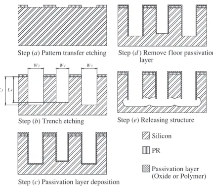
Figure 1. Schematic of the process steps which result in damaged structures caused by corner erosion.
L4
L3
W3
W4
W3
Step (d ) Remove f loor passivation
layer Step (a) Pattern transfer etching
Step (e) Releasing structure
Step (c) Passivation layer deposition Step (b) Trench etching
Silicon PR
Passivation layer (Oxide or Polymer)
Figure 2. Schematic of the typical process steps which can effectively avoid the corner erosion shown in figure1. The key is to make the widths of the trench openings very close to each other. However, the maximum in-plane displacement of the suspended structures are limited to W3.
words, these processes require a thin-film deposition step and a pattern transferring step (lithography and RIE). Furthermore, for these processes, it is relatively difficult to successfully fabricate suspended HARS if the maximum width of trench opening is relatively large. The explanation is described as follows: figure1shows the typical process steps for fabricating suspended HARS using the sidewall protection layers. Step (a) is the patterning for ICP etching mask. Step (b) is the trench etching. Before releasing the suspended structure by isotropic silicon etching, the sidewalls of the structure have to be protected by depositing the passivation layers (polymer or oxide), as shown in step (c). Since W1 is much greater
than W2, the trench aspect ratio in region I is much less than that in region III. Note that here we define the trench aspect
ratio as the ratio of the trench depth to the trench opening
width. Therefore, the deposition rate in region I is higher than that in region III due to the conductance effect [10,11] and
the reactant transport effect [12]. As a result, the passivation layer in region I is thicker than that in region III. On the other hand, the thickness of the passivation layer in region II is very close to that in region I. In step (d), the passivation layer at the bottom of each trench is removed so that the suspended structure can be ready to be released by isotropic etching. This step will also remove part of the passivation layer on trench
tops. However, as shown in the figure, since the thicknesses of the passivation layers in regions I and II are quite close, the etching of step (d) frequently creates corner erosion on the top edges of trenches, especially when the passivation layers in region I have to be removed completely. These corner
erosions result in damage to the suspended structures during
the structure-releasing process, as shown in step (e).
The typical process to avoid the corner erosion is shown in figure2. The key is to make the widths of the trench openings very close to each other (i.e. W3∼= W4) so that the thickness of the passivation layer on the bottom floor of each trench will be very close. However, as shown in figure2, the maximum in-plane displacement of the suspended structures will be limited to W3. On the other hand, an oxide/nitride etching mask may also resolve this problem, but an extra deposition process as well as a pattern transferring process (lithography and RIE) is required.
In this work, we present an ICP–RIE process that employs the characteristic of the microtrenching effect [13] to fabricate suspended HARS. The microtrenching effect can be enhanced by using special ICP etching parameters. Since the proposed fabrication process has no constraints on the design of the width of trench openings, the fabricated devices by this process can be used for applications which require large in-plane displacement. Furthermore, all the process steps can be integrated as a single-run single-mask ICP–RIE process, which makes this proposed technique simple and inexpensive. This paper is organized as follows: the proposed fabrication process for suspended structures is described in section2. In section3, we discuss the considerations and the results of the fabrication process. In section4, we propose an isolation process for the electrical isolation. The conclusion of this paper is presented in section5.
2. The fabricating process for suspended structures with a large width of trench opening and a large trench aspect ratio
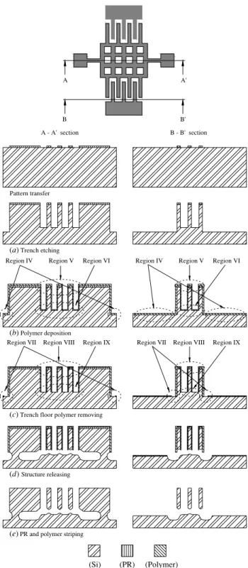
In this section, we will present the process for fabricating suspended MEMS structures that have large widths of trench opening by using a single-run ICP process. As shown in figure3, the steps of the single-run ICP process are in fact the variants of the etching and passivation steps of the standard BOSCH process. The detailed description of each step is as follows.
2.1. Patterning of etching mask
Before the ICP–RIE process, photoresist is spun and patterned as the etching mask for deep silicon etching.
Step (a). Trench etching. The standard BOSCH process is
applied to etch the exposed silicon to a desired depth.
Step (b). Polymer deposition. A fluorocarbon polymer layer
is deposited around the structure surfaces so that the sidewalls of trenches will be protected during the following releasing step. Due to the conductance effect [10,11] and the reactant
transport effect [12], the CF deposition flux distribution is affected by the width of trench opening and the trench aspect ratio. The larger the width of trench opening, the larger
Region VII Region VIII Region IX Region IV Region V Region VI Region VI Region V Region IV Pattern transfer (Polymer) (PR) (Si) (b) Polymer deposition
(c) Trench floor polymer removing (a) Trench etching
B - B' section A - A' section B' B A' A Region IX Region VIII Region VII (d) Structure releasing
(e) PR and polymer striping
Figure 3. The schematic of the steps of the proposed fabrication process.
the polymer deposition rate at the trench bottom. Similarly, the smaller the trench aspect ratio, the larger the polymer deposition rate at the trench bottom. Therefore, as shown in figure 3, since the trench aspect ratio at region IV is smaller than that at region VI, the bottom passivation layer thickness at region IV is more than that at region VI. Note that the polymer thickness at region V is similar to that at region IV. It is worthwhile to note that when using the polymer deposition recipe shown in table 1 to fabricate a
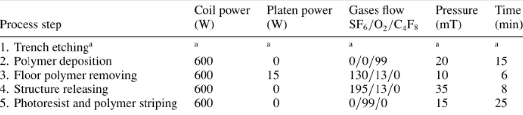
Table 1. The recipe used for fabricating the device shown in figure6.
Coil power Platen power Gases flow Pressure Time
Process step (W) (W) SF6/O2/C4F8 (mT) (min)
1. Trench etchinga a a a a a
2. Polymer deposition 600 0 0/0/99 20 15
3. Floor polymer removing 600 15 130/13/0 10 6
4. Structure releasing 600 0 195/13/0 35 8
5. Photoresist and polymer striping 600 0 0/99/0 15 25
aThe trench etching recipe is standard and can be obtained from the ICP–RIE vendor.
structure with 50 µm in thickness (the trench aspect ratio is 10), the polymer thickness on the top of the structure is 2.6 µm and the polymer thickness at the trench bottom is 0.19 µm.
Step (c). Floor polymer removing. This step is similar to
the etching step of the standard BOSCH process, except that the time for floor polymer removal is a few minutes. The etchant, which consists of fluorine and oxygen radicals, is used to remove the floor polymer with the assistance of ion bombardment. The floor polymer layers in region IX can be easily removed completely because they are thinner. On the other hand, because of the microtrenching effect [13], the etching rate at the corners of the trench bottom is larger than that at the center of the trench bottom. Therefore, for those regions with smaller trench aspect ratio (i.e. the floor polymer layers are relatively thick in these regions), only the polymer at the corners of the trench bottom is removed (as indicated by region VII). More discussions on the enhancement of the microtrenching effect will be provided in section 3. The polymer etching time has to be controlled carefully so that the polymer in region IX is removed completely and only part of the polymer in region VIII is removed, which in turn avoids
corner erosion on the top edges of each structure.
Step (d). Structure releasing. In this step, the exposed silicon
is isotropically etched using the etching step of the BOSCH process. The purpose of this step is to release structures.
Step (e). PR and polymer striping. In this step, most of the photoresist and the passivation layers can be removed by oxygen plasma.
Note that the definition of the conductance in vacuum physics is in fact the ratio of gas flow and pressure differential ([10], pp 87–88). For a given gas, flowing at a given temperature, the conductance is dependent only on the geometry of the trench. The details can be found in [10,11]. Generally speaking, the conductance decreases as the trench aspect ratio increases. Therefore, the conductance of the etching/depositing species influences an etching/deposition process by limiting the flux of the etching/deposition species arriving at the bottom of the feature where the process takes place. In other words, at the same reaction probability of sidewall, as the trench aspect ratio increases, the reactant flux to the feature bottom will decrease, which in turn decreases the etching/deposition rate at the trench bottom.
Also note that the reactant transport effect describes the influence of the transport of ions and neutral species on the etching rate at the bottom of rectangular trenches [12]. Under the typical process conditions, the etching rate depends strongly upon the ion flux because of the low fluorine reaction
probability and the low reactant depletion within the feature. When the trench aspect ratio increases, the ratio of the flux to the trench bottom and the flux to the sidewall decreases, and hence the etching/deposition rate on the trench also decreases. 3. Process considerations and results
In section2, we have proposed the process, which employs the
etching and passivation steps of the standard BOSCH process,
to fabricate released HARS with large widths of trench opening using a single-run ICP process. In this section, we will present the process results and provide discussions and considerations for the process.
3.1. Considerations for polymer deposition
The process uses a polymer layer to avoid sidewall erosion during the following floor polymer removing step and the structure releasing step. Due to the conductance effect [10, 11] and the reactant transport effect [12], the flux distribution of CF-based species around a trench profile is affected by the width of the trench opening and the aspect ratio of the trench. For the cases where the width of the trench opening is large or the trench aspect ratio is small, the polymer deposition rate is large at the trench bottom. As shown in step (b) of figure3, because the trench aspect ratio in region IV is smaller than that in region VI, the bottom passivation layer thickness in region IV is more than that in region VI, and is almost the same as the thickness at region V.
If the deposited polymer thickness is relatively small (i.e. the polymer thickness on region V is about 1.1 µm), the differences of polymer thicknesses between regions IV, V and VI are also small (smaller than 0.9 µm). When removing the floor polymer at region VI, the time must be very accurate. Otherwise, it is very likely that the polymer layer at region V will also be removed, and then corner erosion is created. On the other hand, if the deposited polymer thickness is relatively large (i.e. the polymer thickness in region V is about 2.6 µm), the difference in polymer thicknesses in regions VI and V will also be relatively large (larger than 2.3 µm), which implies that the difference of the times for removing the polymer at regions VI and V is also large. Under this condition, it is much easier to control the etching time for achieving the desired etching condition in which the floor polymer is effectively removed without creating corner erosion.
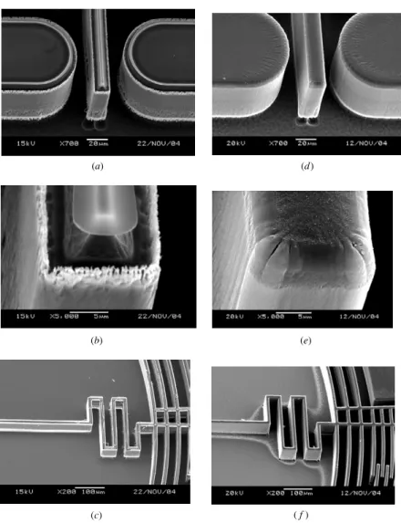
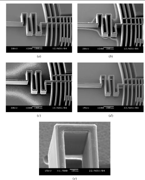
Figure4shows SEM pictures of the top of the structures after the floor polymer removal step. In figures 4(a)– (c), the original deposited polymer thickness on the top of the structure is 1.1 µm. In figures 4(d)–(f ), the original deposited polymer thickness on the top of the structure is
(a) (d)
(b)
(c)
(e)
( f )
Figure 4. SEM pictures which show the top of the structures after the floor polymer removal step. (a)–(c) The original deposited polymer thickness on the top of the structure is 1.1 µm. (d)–(f ) The original deposited polymer thickness on the top of the structure is 2.6 µm. (b) and (c) are the closer views of (a) and (d), respectively. The floor polymer removal times (etching times) are the same for all the figures. Note that the parameters for depositing the polymer are as follows: the coil power is 600 W, the C4F8flow rate is 99 sccm and the pressure is
20 mT. The parameters for floor polymer removing are as follows: the coil power is 600 W, the platen power is 10 W, the SF6flow rate is
130 sccm, the O2flow rate is 13 sccm, and the pressure is 10 mT.
2.6 µm. Figures 4(b) and (e) are the closer views of figures4(a) and (d), respectively. The floor polymer removal times (etching times) are the same for all the figures. The structure thickness is 50 µm. In figures 4(a)–(c), because the originally deposited polymer thickness is insufficient, the top surfaces of the structure are damaged (corner erosion). Figures4(d)–(f ) show the cases in which the floor polymer at the base (bottom corner) of the structures is removed without damaging the top surfaces of the structures. Note that the parameters for depositing the polymer are as follows: the coil power is 600 W, the C4F8flow rate is 99 sccm and the pressure is 20 mT. The parameters for floor polymer removing are as follows: the coil power is 600 W, the platen power is 10 W, the SF6flow rate is 130 sccm, the O2flow rate is 13 sccm, and the pressure is 10 mT.
3.2. Considerations for floor polymer removing
This step (step (c) in the previous section) is a combination of physical (ion) bombardment and chemical reaction using fluorine radicals. Only the ion bombardment is dominant
for this etching step [14]. Therefore, the probability of ion bombardment on the sidewall polymer has to be reduced so that the sidewall polymer will not be etched simultaneously. However, because of the microtrenching effect [13], the etching rate at the corners of a trench bottom is larger than that at the center of the trench bottom. It is believed that the
microtrenching effect is produced by the reflection of ionized
particles off the sidewalls, which in turn leads to ‘focusing’ of particles at the base of the sidewalls, giving rise to higher etch rates. Our experiment shows that the microtrenching effect can be enhanced by increasing the platen power and reducing pressure. Figure 5 presents the process characteristics for different platen powers and pressures. Figure 5(a) shows the SEM picture of the structure for 10 W platen power and 30 mT pressure. In this case, the floor polymer is thoroughly removed only in the regions with relatively high trench aspect ratio. As the pressure is reduced, more floor polymer can be removed, as shown in figure5(b) (i.e. 10 W platen power and 10 mT pressure). In figure5(c), increasing platen power (15 W) also helps increase the effectiveness of removing the
(a) (b)
(c) (d)
(e)
Figure 5. Floor polymer removal conditions using the different platen powers and pressures. (a) The platen power is 10 W and the pressure is 30 mT. (b) The platen power is 10 W and the pressure is 10 mT. (c) The platen power is 15 W and the pressure is 30 mT. (d) The platen power is 15 W and the pressure is 10 mT. (e) The closer view of (d). Note that the parameters for floor polymer removing are as follows: the coil power is 600 W, the SF6flow rate is 130 sccm and the O2flow rate is 13 sccm. The parameters for depositing the polymer are as
follows: the coil power is 600 W, the C4F8flow rate is 99 sccm and the pressure is 20 mT.
floor polymer. With 15 W platen power and 10 mT pressure, the polymer on the top and at the bottom of the structure is removed completely, as shown in figure5(d). However, in this case, corner erosion occurs on the top surface of the structure (figure5(e)). Note that in figure5the structure thickness is 50 µm.
3.3. Considerations for structure thickness
For the same pattern design (i.e. using the same mask), increasing structure thickness also increases the trench aspect ratio. Therefore, the process parameters for the steps of polymer deposition and structure releasing must also be modified. In the polymer deposition step, the CF deposition rate near the trench bottom decreases as the trench aspect ratio increases. In order to retain sufficient thickness of the polymer on the sidewalls of trenches, the polymer deposition time should also be increased with the trench aspect ratio. Besides, due to the conductance effect [10,11] and the reactant
transport effect [12], the flux distribution of etchants around a trench profile is affected by the width of the trench opening and
Figure 6. The fabricated circular electrostatic rotary structure with 50 µm thickness.
the aspect ratio of the trench. Hence, in the structure-releasing step, the lateral etching rate decreases as the trench aspect ratio
(a)
(b)
Figure 7. (a) The fabricated comb-drive structure with 100 µm thickness by the novel process. (b) Close-up view of the structure.
increases. Therefore, the etching time for structure releasing also increases with the trench aspect ratio.
3.4. Process results
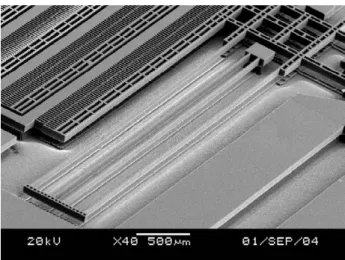
In this subsection, we demonstrate that the process proposed can be used to fabricate structures with high aspect ratio, large thickness, and large widths of trench opening. In other words, these devices can potentially be used for application of a large in-plane displacement. Figure6shows the SEM picture for a circular electrostatic rotary structure. The structure thickness is 50 µm and the maximum trench aspect ratio is 10. The recipe is shown in table1. Figures7and8show a suspended comb-drive structure with 100 µm thickness. The maximum trench aspect ratio is 20. The corresponding recipe is listed in tables2and3, respectively. Figure9shows a suspended comb-drive structure, which can potentially be used for large-displacement motions (over 100 µm). The thickness of the actuator is 100 µm, and the beam width is 15 µm. The maximum trench aspect ratio is 20, and the longest length of the suspended beam is 2 mm. The corresponding recipe is listed in table3.
(a)
(b)
Figure 8. (a) The fabricated comb-drive structure with 100 µm thickness by the novel process. (b) Close-up view of the structure. Note that the process parameters used for this figure are different from those for figure7.
Figure 9. The long suspending folded beam with 2 mm length, 15 µm width and 120 µm thickness.
4. The proposed electrical isolation process
For MEMS actuators and sensors, electrostatic actuation and capacitive sensing are the most popular methods. However,
Region X
Closer View of Region XIV Cl
C oser View of Region XI
Region XIII Region XII
Region XI Region X
Step (a) Oxidation
Step (b) Poly-Si deposition + dopping
Step (c) Remove floor Poly-Si
Step (d ) Al sputtering (Metal) (Oxide) (Poly-Si) (Si) B - B' section A - A' section Region XIV
Closer View of Region XIII Region XII
Figure 10. The triple-layer electrical isolation method.
Table 2. The recipe used for fabricating the device shown in figure7.
Coil power Platen power Gases flow Pressure Time
Process step (W) (W) SF6/O2/C4F8 (mT) (min)
1. Trench etchinga a a a a a
2. Polymer deposition 600 0 0/0/99 20 25
3. Floor polymer removing 600 15 130/13/0 10 7.5
4. Structure releasing 600 0 195/13/0 35 15
5. Photoresist and polymer striping 600 0 0/99/0 15 25
aThe trench etching recipe is standard and can be obtained from the ICP–RIE vendor.
Table 3. The recipe used for fabricating the device shown in figures8and9.
Coil power Platen power Gases flow Pressure Time
Process step (W) (W) SF6/O2/C4F8 (mT) (min)
1. Trench etchinga a a a a a
2. Polymer deposition 600 0 0/0/99 20 25
3. Floor polymer removing 600 15 130/13/0 10 8
4. Structure releasing 600 0 195/13/0 35 15
5. Photoresist and polymer striping 600 0 0/99/0 15 25
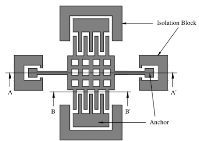
Anchor Isolation Block B' B A' A
Figure 11. The layout of the isolation block and anchor.
the required voltages for electrostatic actuation typically are at least tens of volts or beyond hundred volts. Therefore, it is critical to have a proper electric isolation for fabricated structures. A few isolation processes have been proposed, such as the method proposed in the SCREAM process [3], the junction isolation process [8], the trench-filled isolation process [4,15,16] and the triple-layer isolation method [17].
The SCREAM process uses the sputtering metal layer as a conductive layer. As the depth/width ratio of a trench is larger than five, the poor conformality of the metal sputtering process will not be able to give a uniformly-deposited layer on the sidewalls of microstructures. In the junction isolation method, the electrical isolation is accomplished by a reverse-bias voltage between the counter-doped electrodes and the substrate. However, it is difficult to completely dope a very thick structure so that a high lateral capacitance between the electrodes cannot be obtained. The trench-filled isolation process uses oxide or nitride as the insulting layer between the electrode and the substrate. However, it requires two separate processes and two masks.
For high-aspect-ratio MEMS structures (the typical depth/width ratio of a trench larger than 5, the focus of this work), the electrical isolation can be realized by using the triple-layer isolation method [17] (as shown in figure10) incorporated with an isolation block around each anchor (as shown in figure11). The details of the triple-layer isolation method are described as follows.
In step (a), the process starts with the oxidation of all exposed surfaces and then the deposition of heavily doped LPCVD polysilicon follows, as shown in step (b). The insulating thermal oxide we used is about 0.12 µm and the temperature used for the thermal isolation oxide is 1080◦C. The thickness of polysilicon is 0.18 µm and the residual stress is 30 MPa. In step (c), the floor polysilicon is removed using the BOSCH process. Note that inside the undercuts of regions X and XI, the doped polysilicon still remains. In this step, the polysilicon layer on the top side of the structure was also removed. Hence, an Al film was sputtered to cover the top and sidewall of the structure (figure 10(d)). Because the conformity of sputtering processes is poor, for the structures with the trench aspect ratio of greater than 5, the aluminum layer covers only the upper part of sidewalls (as shown in region XII) without reaching the trench bottom, which indicates the electrical isolation still remains, as shown in the closer views of regions XIII and XIV of figure10.
However, it is still very possible that the substrate and the suspended structure will be electrically short around the anchors. Therefore, isolation blocks, as shown in figure11, are proposed. An isolation block can create a narrow gap around the anchor. The gap can effectively prevent the sputtered aluminum film from shortening the movable structure and the substrate, as shown in region XI of figure10.
5. Conclusion
In this work, we present a novel process for fabricating high-aspect-ratio suspended structures with the large width of trench openings. Using the microtrenching effect, we successfully used photoresist as an etching mask for releasing suspended structures without thoroughly removing the floor polymer in regions with small trench aspect ratio. The steps for trench etching, sidewall passivation, structure releasing and PR/polymer striping can be integrated as a run single-mask ICP–RIE process, which effectively reduces the process complexity and fabrication cost. The considerations for each process step and the phenomenon of corner erosion, which result in undesired etching of the silicon structure during the releasing step, are also discussed in detail. Using the proposed process, suspended structures with the maximum thickness of 100 µm and the maximum aspect ratio of 20 are demonstrated. Also, the proposed process can be used to fabricate the devices for large in-plane-displacement applications.
Acknowledgment
This work is supported by the National Science Council, Taiwan, ROC (contract no NSC 93 2212 E 002 023). The authors would like to thank Mr Hsin-Hong Liao for his help in the fabrication process.
References
[1] Laermer F and Schilp A Method of anisotropically etching silicon US Patent No 5501893
[2] Diem B, Delaye M T, Michel F, Renard S and Delapoerre G 1993 SOI(SIMOX) as a substrate for surface
micromachining of single crystalline silicon sensors and actuators Digest Technical Papers in Proc. 7th Int. Conf. on
Solid-State Sensors and Actuators (Transducers ’93) (Yokohama, June 1993) pp 233–6
[3] Shaw K A, Zhang Z L and MacDonald N C 1994 SCREAM I: a Single mask, single-crystal silicon, reactive ion etching process for microelectromechanical structures Sensors
Actuators A 40 63–70
[4] Sarajlic E, de Boer M J, Jansen H V, Arnal N and Puech M 2004 Advanced plasma processing combined with trench isolation technology for fabrication and fast prototyping of high aspect ratio MEMS in standard silicon wafers
J. Micromech. Microeng. 14 S70–5
[5] Bertz A, Kuechler M, knoefler R and Gessner T 2002 A novel high aspect ratio technology for MEMS fabrication using standard silicon wafers Sensors Actuators A 97–98 691–701 [6] Park S, Lee S, Yi S and Cho D 1999 Mesa-supported, single
crystal microstructures fabricated by the surface/bulk micromachining process Japan. J. Appl. Phys. 38 4244–9 [7] Lee S, Park S, Yi S, Lee S and Cho D D 1999 Electrostatic
actuation of surface/bulk micromachined single-crystal silicon microresonators Proc. the 1999 IEEE/RSJ Int. Conf. on Intelligent Robots and System (Las Vegas, NV, October 1999) pp 1057–62
[8] Lee S, Park S and Cho D 1999 The surface/bulk micromachining (SBM) process: a new method for fabrication released MEMS in single crystal silicon
J. Microelectromech. Syst. 8 409–16
[9] Hsieh J and Fang W 2002 A boron etch-stop assisted lateral silicon etching process for improved high-aspect-ratio silicon micromachining and its applications J. Micromech.
Microeng. 12 574–81
[10] Dushman S and Lafferty J M 1962 Scientific Foundations of
Vacuum Technique 2nd edn (New York: Wiley) p 94
[11] Coburn J W and Winters H F 1989 Conductance
considerations in the reactive ion etching of high aspect ratio features Appl. Phys. Lett. 55 2730–2
[12] Arnold J C, Gary D C and Sawin H H 1993 Influence of reactant transport on fluorine reactive ion etching of deep trenches in silicon J. Vac. Sci. Technol. B 11 2071–80
[13] Hoekstra R J and Kushner M J 1998 Microtrenching resulting from specular reflection during chlorine etching of silicon
J. Vac. Sci. Technol. B 16 2102–4
[14] Rangelow I W 2001 Dry etching-based silicon micro-machining for MEMS Vacuum 62 279–91 [15] Lee S, Park S, Cho D and Oh Y 1999 Surface/bulk
micromachining (SBM) process and deep trench oxide isolation method for MEMS Technical Digest IEEE
Electron Devices Meeting (IEDM’99) (Washington, DC, December 1999) pp 701–4
[16] Lee S C, Park S and Cho D D 2002 Honeycomb-shaped deep-trench oxide posts combined with the SBM technology for micromachining single-crystal silicon without SOI Sensors Actuators A 97–98 734–8 [17] Lee S, Park S, Kim J, Lee S and Cho D 2000 Surface/bulk
micromachined single-crystalline-silicon micro-gyroscope