Shih-Cheng Lin, Chi-Hsueh Wang, and Chun Hsiung Chen, Fellow, IEEE
Abstract—A novel patch-via-spiral resonator based on the dual-metal-plane configuration is proposed and examined. With the microstrip patch on the top plane serving as a capacitor and linking to the quasi-lumped spiral inductor on the bottom plane through a connecting via, the proposed dual-plane resonator structure located on the opposite sides of the single substrate may form a miniaturized one in the printed-circuit board fab-rication. By suitably combining the proposed patch-via-spiral resonators, useful coupled-resonator pairs may be constructed to simultaneously provide electric and magnetic couplings. Based on these coupled-resonator pairs, a second-order bandpass filter with multiple transmission zeros is realized without requiring either the cross-coupled path or the source–load coupling. For design purpose, the equivalent-circuit model is also derived and verified. In this study, a fourth-order patch-via-spiral bandpass filter with both good passband selectivity and miniaturized size of only 22.14 mm 5.08 mm (i.e., 0 188 0 0 043 0) is implemented, where 0 denotes the guided wavelength of the 50- microstrip line at center frequency.
Index Terms—Coplanar waveguide (CPW), coupled-resonator bandpass filter, dual-metal-plane structure, microstrip, miniatur-ization, transmission zero.
I. INTRODUCTION
D
UAL-PLANE configuration has increasingly attracted at-tention in the field of microwave design, especially for the development of mobile communication. Since most mobile de-vices leave limited space for the placement of filters, it is of im-portance to miniaturize the required filter size. In the dual-plane approach, which makes good use of two metal planes on the opposite sides of the single substrate, the arrangement of com-ponents is no longer limited on the single plane and, thus, the design becomes flexible. In addition, the fabricated components will end up with the three-dimensional structure, thus it may re-duce their occupied planar size.Except for the size reduction, transmission zeros are usually required to attenuate the stopband level and also to sharpen the passband response. Several topologies, which are capable of creating transmission zeros around the passband, were pre-sented in the literature [1]–[8]. The topologies such as canon-ical form, cascaded quadruplet [1]–[5], extracted pole [6], and
Manuscript received July 24, 2006; revised September 19, 2006. This work was supported by the National Science Council of Taiwan under Grant NSC 95-2752-E-002-001-PAE, Grant NSC 95-2219-E-002-008, and Grant NSC 95-2221-E-002-196.
The authors are with the Department of Electrical Engineering and Graduate Institute of Communication Engineering, National Taiwan University, Taipei 106, Taiwan, R.O.C. (e-mail: [email protected]).
Digital Object Identifier 10.1109/TMTT.2006.888579
source–load coupling [7], [8] have been successfully realized using the coplanar waveguide (CPW) or microstrip structure. The above-mentioned planar filters are all fabricated on one plane of the single substrate and, thus, may occupy larger space. Over the past few years, several research studies have been reported to implement the filter topologies in the dual-plane configuration so as to economize the occupied size of filters. In a general sense, the dual-plane configuration may be classified into two principal catalogs. One catalog takes advantage of metallization patterns among two dielectric substrates with a common ground. Quarter-wavelength resonators are allocated on the outer planes of two substrates and the nonadjacent cross coupling is realized through the slots on the common ground [9]. Furthermore, microstrip open-loop resonators that lie on outer sides of two substrates with a common ground in between are coupled by the apertures on the ground so as to provide both electric and magnetic couplings for specified filtering charac-teristics [10], [11]. The filters belonging to this catalog need to tightly combine two dielectric substrates together, thus they require a complicated fabrication process to achieve high preci-sion. The other catalog utilizes two metal planes on the opposite sides of a single substrate. Suspended-stripline filters were pre-sented in [12] by arranging the quasi-lumped resonators in either an antipodal or parallel way. The main drawback of using a suspended stripline is the requirement of critical housing tech-nology. Double-surface CPW filters [13] were constructed by introducing an electrode pattern on a double-sided metallized substrate with a high dielectric constant. A dual-plane combline filter having plural attenuation poles was investigated in [14]. However, the input and output ports are connected to CPW lines by tapped wires, which are hard to control accurately, and the analysis method is complicated when applied to higher order filters. An ultra-wideband bandpass filter based on the microstrip-to-CPW transitions and CPW/microstrip shorted stubs connected to ground was introduced [15]. However, its transmission zeros on the upper stopband are generated through complicated resonant mechanisms, therefore, it is difficult to establish the guidelines for designing such a filter. Another ultra-wideband filter using the hybrid microstrip and CPW structure in a dual-plane configuration was also presented in [16]. The CPW bandpass filters using both loaded air-bridge enhanced capacitors and broadside-coupled transition struc-tures for wideband spurious suppression was recently proposed in [17] by also making use of dual-plane configuration without introducing any transmission zeros around the passband.
In this study, novel patch-via-spiral resonators fabricated in the dual-metal-plane configuration are proposed and utilized
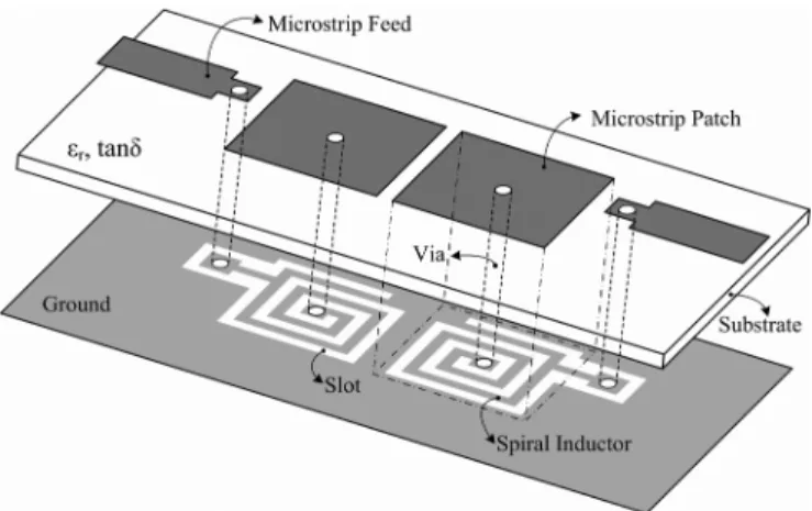
Fig. 1. Three-dimensional geometry of the proposed second-order filter using patch-via-spiral resonators in the dual-plane configuration.
to achieve both filter-size miniaturization and transmission zeros creation originated from a completely different coupling scheme. The microstrip patches of the coupled-resonator pair on the top plane provide the electric coupling, while the spiral inductors on the bottom plane offer the mutual magnetic coupling. The simultaneously existed electric and magnetic couplings in a coupled-resonator pair facilitate the design of direct-coupled filters with transmission zeros, but without introducing either cross-coupling between nonadjacent res-onators or source/load coupling between input/output ports. Based on the single patch-via-spiral resonator, several types of coupled-resonator pairs are carefully investigated and char-acterized. These coupled-resonator pairs are then applied to design miniaturized filters with prescribed frequency responses. For instance, the second-order filter (Fig. 1) may be realized for an elliptic-like or Chebyshev response by using different types of coupled-resonator pairs. By appropriately integrating the different types of coupled-resonator pairs, one may implement a higher order filter with improved performance. Specifically, the fabricated fourth-order filter provides sharp selectivity and possesses a miniaturized size of only 22.14 mm 5.08 mm (i.e., ). The good performance of the proposed filter using patch-via-spiral resonators makes it a useful component for the wireless system.
II. PATCH-VIA-SPIRAL RESONATORS IN
DUAL-PLANECONFIGURATION
Shown in Fig. 2(a) is the three-dimensional geometry of the proposed patch-via-spiral resonator. The top- and bottom-plane layouts viewed from the bottom side are also depicted in Fig. 2(b). The newly proposed resonator is mainly composed of three elements, i.e., the microstrip patch on the top plane, the connecting via through the substrate, and the grounded spiral inductor on the bottom plane. The microstrip patch has rectangle shape with area . The via-hole is drilled by the 1-mm-diameter bit and filled with the conductive liquid silver to provide good connecting capability. The spiral on the bottom-plane of length is covered by the patch on the top plane. Note that the spiral is short circuited to the CPW ground. This novel structure may roughly be regarded as a combination of quasi-lumped capacitors and inductors, as
Fig. 2. Proposed patch-via-spiral resonator structure. (a) Three-dimensional geometry. (b) Top- and bottom-plane layouts. (c) Equivalent-circuit model. With the structure looking from the bottom and shown in (b), the gray region denotes the spiral inductor and ground on the bottom plane, and the dashed line repre-sents the rectangle microstrip patch on the top plane.
shown in Fig. 2(c). Since the elements of the patch-via-spiral resonator are located on the opposite sides of single substrate, its occupied size may be miniaturized. The dimensions of major resonator parameters, such as the patch area, spiral linewidth, and spiral line length, to provide a given response, are basically affected by the substrate. To be specific, hereafter, all circuits in this study will be fabricated on an FR4 board ( ,
mm, ).
The approximate lumped-element equivalent circuit of the proposed resonator is presented in Fig. 2(c). Here, indicates the portion of the spiral inductance in the vicinity of the CPW ground, while denotes the rest of the spiral inductance measured from the via-hole location. The portion of the patch overlapping the spiral is represented by the capacitance shunt with the inductance ; while the rim of patch forms the parallel-plate capacitance to the ground. Note that the spiral on the bottom-plane contributes towards the total inductance of . Although the models of shorted resonators with grounding vias [18] were proposed and the spiral inductors for filter application [19] were also reported, the proposed patch-via-spiral resonator has a complicated composite struc-ture, which is hardly analyzed using closed-form formulas. The microstrip patch and spiral inductor are strongly coupled to each other, thereby becoming inseparable. The corresponding lumped-element circuit model may be extracted using the quasi-static method-of-moment simulator (Ansoft Q3D v6.0).
Fig. 3. Resonant frequencies with respect to different sets of physical dimen-sions (in millimeters) for the single patch-via-spiral resonator presented in Fig. 2, whereW and D are given in parentheses, respectively.
To characterize this structure and to get its corresponding fre-quency characteristics, the full-wave electromagnetic simulator (Ansoft Designer v2.0) is also used.
The patch-via-spiral resonator is carefully designed and ad-justed to provide the resonant frequency at 1.43 GHz. To this end, the physical dimensions of the resonator are given as
mm, mm, mm, and
mm. Therefore, the extracted lumped-element values are nH, pF, and pF, respectively. With the favor of a dual-plane configuration, the novel patch-via-spiral resonator is compact and has a size of only 5.08 mm 5.08 mm (i.e., ).
Using the weakly capacitive-gap-coupled excitation and the extraction technique provided in [20], the unloaded quality factor associated with the proposed resonator is found about 60, a value comparable to the conventional microstrip distributed-element resonators fabricated on the same FR4 substrate. The influence of the via on is also examined by varying the via diameter from 0.15 to 7.62 mm and, even so, the corresponding values are found nearly constant.
To characterize the proposed resonator, the fundamental res-onant frequency is simulated, using different sets of physical dimensions of the resonator. The simulated transmission coef-ficients are illustrated in Fig. 3. Intuitively, the larger the area of the microstrip patch, the larger the loaded capacitance for the resonator and, thus, the lower the resonant frequency.
III. COUPLED-RESONATORPAIRS
Two patch-via-spiral resonators may properly be arranged to form the required coupled-resonator pairs. Shown in Fig. 4 are two possible types of coupled-resonator pairs with the tapped-line-fed structures included for realizing the second-order filters discussed below.
Fig. 5(a) shows the conventional coupling and routing dia-gram for these coupled-resonator pairs (Fig. 4). The coupling between two resonators is simply modeled by the overall coupling coefficient . However, two coupled paths pro-viding electric coupling and magnetic coupling may be realized by the proposed coupled-resonator pairs in Fig. 4(a) and (b). Fig. 5(b) shows a decomposed coupling diagram with divided into and . By utilizing
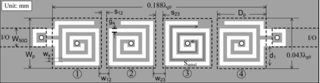
Fig. 4. Top- and bottom-plane layouts of the proposed coupled-resonator pairs. (a) Symmetric type1 [S1]. (b) Flipped type1 [F1]. (W = 1:93, g = 0:7, d = 3:3, g = 0:38, w = 0:38, W = 5:08, L = 5:08, s = 0:53, w = 1:04. Unit: millimeters).
Fig. 5. (a) Overall and (b) decomposed coupling and routing diagrams of the coupled-resonator pair.
the decomposed coupling diagram exhibited in Fig. 5(b), a filter may be designed to introduce a pair of transmission zeros without adopting the conventional cross-coupling or source–load coupling. In this diagram, two out-of-phase cou-plings, which simultaneously exist between the two coupled resonators, are essential in achieving the specified filtering re-sponse, as mentioned in [12]. Once the out-of-phase condition is met, the direct-coupled filter with an elliptic-like response may be realized. In contrast, a Chebyshev response may al-ternatively be achieved by creating the in-phase couplings. Since the proposed resonator is composed of a microstrip patch on the top plane and a spiral inductor on the bottom plane, one can easily arrange a coupled-resonator pair to provide an electric coupling path along the top plane and another magnetic coupling path along the bottom plane.
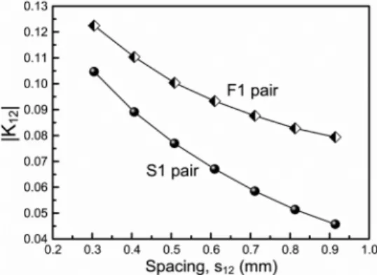
The principal difference between Fig. 4(a) and (b) is reflected by the spiral-wound direction. Among the symmetric-type1 coupled-resonator pair shown in Fig. 4(a) (hereafter simply denoted as the S1 pair), the spiral inductors of the coupled resonators are wound in the opposite directions. Conversely, the spiral inductors in the flipped-type1 coupled-resonator pair shown in Fig. 4(b) (simply denoted as F1 pair) are wound in the same direction. In order to design the filters using dif-ferent types of coupled-resonator pairs, the overall coupling
Fig. 6. Simulated overall coupling coefficients for the S1 and F1 pairs in Fig. 4(a) and (b), respectively.
Fig. 7. Field distributions and current flows along the spiral inductors be-longing to coupled-resonator pairs. (a) S1. (b) F1.
coefficients as functions of gap spacing for the two coupled-resonator pairs [see Fig. 4(a) and (b)] are illustrated in Fig. 6 according to the information of resonant-mode splitting [2]. One can easily observe that the overall coupling for the F1 pair is larger than that for the S1 pair. It implies that the electric and magnetic couplings tend to add in the F1 pair, while tending to cancel in the S1 pair.
Physically, the signs of electric and magnetic couplings may be distinguished by an approach extended from Zhang et al. [21]. Fig. 7 illustrates the field distributions and current flows along the spiral inductors belonging to two distinct coupled-res-onator pairs. In our proposed coupled-rescoupled-res-onator pair, the overall coupling may be divided into two different parts, i.e., the cou-pling between the microstrip patches and that between the spiral inductors .
The coupling between the microstrip patches on the top plane may roughly be written as
(1)
The coupling between the spiral inductors on the bottom
plane may also be expressed as
(2)
Here, and denotes the vector electric fields belonging to the microstrip patches of resonators 1 and 2, while and are the vector magnetic fields resulting from the spirals. The volumes of the air, substrate, and whole infinity space are denoted by , , and , respectively. Note that sub-scripts and denote the patch and spiral, while the and represent electric and magnetic, respectively. On the top plane, the electric coupling dominates the interaction between two patches, thus the term in (1) corresponding to magnetic fields may approximately be neglected . Moreover, the two spirals on the bottom plane of the two patch-via-spiral resonators are so distant that their magnetic fields are dominant in evaluating ; equivalently it implies that .
For the S1 pair [see Fig. 4(a)] with the spirals wound in op-posite directions, the dot product of electric fields will always be positive, as observed from Fig. 7(a), resulting in a negative value for . When the two spirals are wound in the opposite directions, the currents in the spiral windings will be in the opposite directions as well. This makes the dot product of magnetic fields and positive . Thus, the cou-plings between patches and spirals will be out-of-phase. Con-versely, for the F1 pair Fig. 4(b) with the two spirals wound in the same direction, the couplings between patches and spi-rals will be in-phase . The in-phase couplings among the F1 pair brings about a larger overall coupling coeffi-cient than that of the S1 pair, as depicted by the curves in Fig. 6. According to the above-mentioned argument based on the field expressions in (1) and (2), one may relate the coupled res-onator structure exhibited in Fig. 4(a) to the decomposed cou-pling diagram depicted in Fig. 5(b). The coucou-pling between microstrip patches realizes the electric coupling , while the coupling between spiral inductors achieves the required mag-netic coupling .
Furthermore, another two coupled-resonator pairs are also de-picted in Fig. 8(a) and (b) to facilitate the design of the higher order filter. Fig. 8(a) exhibits the so-called symmetric-type2 (S2) coupled-resonator pair, which has the two spirals wound in the opposite directions. In contrast, the two spirals among the flipped-type2 (F2) shown in Fig. 8(b) are wound in the same di-rection. The same argument may be applied to verify the out-of-phase couplings among the S2 pair and the in-out-of-phase couplings among the F2 pair. The simulated overall coupling coefficients
Fig. 9. Simulated overall coupling coefficients for the S2 and F2 pairs in Fig. 8(a) and (b), respectively.
TABLE I
SIGNS OF THEELECTRIC ANDMAGNETICCOUPLINGS FOR
DIFFERENTTYPES OFCOUPLED-RESONATORPAIRS
for both coupled pairs as functions of spacing are illustrated in Fig. 9.
In summary, Table I lists the signs of the electric and magnetic couplings, which are concluded from (1) and (2) for the four coupled-resonator pairs exhibited in Figs. 4 and 8.
IV. ANALYSIS OFSECOND-ORDERFILTERS A. Equivalent Circuit
The equivalent circuit required to design the proposed filter and to determine the locations of two transmission zeros will be derived here. Fig. 10(a) shows the approximate lumped-el-ement equivalent-circuit model for the proposed second-order filter using the patch-via-spiral coupled-resonator pairs exhib-ited in Fig. 4. The inductive coupling through the bottom plane between the two spirals of the coupled-resonator pair is denoted by the mutual inductance . Furthermore, the capacitive cou-pling between the two patches on the top plane of the coupled-resonator pair is represented by the mutual capacitance . Due to the symmetry of this configuration, even- and odd-mode analysis may be adopted to discuss this filter.
By placing a virtual open or virtual short in the center refer-ence plane, the even- and odd-mode equivalent-circuit models are illustrated in Fig. 10(b) and (c). The even- and odd-mode input admittances may be formulated as
(3)
(4)
Fig. 10. Equivalent-circuit models for the second-order filter using the pro-posed patch-via-spiral coupled-resonator pairs exhibited in Fig. 4(a). (a) Com-plete model. (b) Even-mode model. (c) Odd-mode model.
The parallel resonances for the two modes occur as
and . Therefore, the even- and odd-mode resonant fre-quencies are given by
(5)
(6) In addition, the transmission zeros would be created when con-dition holds. The lower and higher transmission-zero frequencies and are given by (7) and (8), shown at the bottom of the following page.
For the filter requiring out-of-phase couplings to achieve transmission zeros, a positive mutual inductance
is essential, and this condition may be realized through the symmetric-type coupled pairs. The positive value brings about two real solutions for (7) and (8), which are the two transmission zeros associated with the filter.
On the contrary, condition , which ensures the in-phase couplings between coupled resonators, may be achieved through the flipped-type pairs and, thus, brings about a filter response without transmission zeros. Note that the negative value results in all imaginary solutions when
Fig. 11. Circuit-model simulated results of the equivalent circuit in Fig. 10(a) for differentC values (in picofarads) to adjust the transmission-zero frequen-cies (L = 3:374 nH, L = 9:1 nH, C = 0:524 pF, L = 0:727 nH, C = 0:74 pF).
calculating the transmission-zero frequencies through (7) and (8), implying the disappearance of transmission zeros.
It is worth mentioning that the frequencies of these two trans-mission zeros may simply be altered by varying the values of or . A demonstrated example is exhibited in Fig. 11, with element values given in the caption, by varying the value of , but keeping other elements unaltered. Apparently, the larger the is, the closer the transmission zeros approach the passband edges. However, the bandwidth is almost not affected due to the minor value of .
B. Design Procedure
Based on the even- and odd-mode resonant frequencies de-rived from (5) and (6), the overall coupling coefficient , which is the combination of electric and magnetic couplings between the two coupled resonators, can be calculated by the formula [22]
(9) The required value is simply proportional to the predeter-mined filter bandwidth. In addition, one may also identify the signs of overall couplings by using (9).
Note that the relative locations of even- and odd-mode reso-nances ( and ) are changed when the sign of mutual in-ductance is altered. By applying these two resonant fre-quencies into (9) under two different conditions ( and ), one may infer that will be positive as , while will be negative as . Therefore, the sign of the overall coupling of the coupled-resonator pair is principally
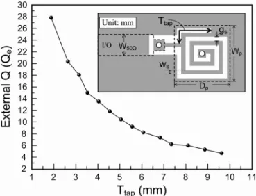
Fig. 12. External quality factorQ of the utilized tapped-line-fed structure with respect to the tapped positionT (W = 1:93 mm, W = D = 5:08 mm, g = 0:38 mm, w = 0:38 mm).
dominated by that of the mutual inductance between spi-rals. Inspecting the full-wave simulated characteristics of the four coupled-resonator pairs exhibited in Figs. 4 and 8 and ob-taining the relative locations of and , one may lead to the conclusion that the symmetric-type coupled-resonator pairs (S1 and S2) always give the positive value , while the flipped-type coupled-resonator pairs bring about the nega-tive value .
Consequently, the bandwidth and transmission-zero frequen-cies may be obtained using (5)–(8) derived thus far in this sec-tion. Note that the external quality factor may also be eval-uated [23] from the single tapped-line-fed patch-via-spiral res-onator by using the full-wave simulator. The tapped-line CPW feed is used at input and output ports for this proposed filter, as shown in Fig. 4. Note that the 50- CPW possesses the center-conductor width of 5.08 mm, for a given slot width of 0.38 mm, which is too wide to serve as the tapped-feed line for the miniaturized patch-via-spiral resonator. To avoid this diffi-culty, a via-connected microstrip-to-CPW transition [24] is de-signed to connect the 50- microstrip line to the tapped-fed CPW with center-conductor width of 0.38 mm. The adoption of this transition would not affect the filter response. The evalu-ated of the proposed resonator is plotted with respect to the tapped position in Fig. 12 in order to facilitate the prac-tical design procedure.
Until now, the required coupling coefficients ’s, external quality factor , and transmission-zero frequencies can all be obtained from either the full-wave simulator or the
equivalent-(7) (8)
2) Obtain the corresponding element values , , , , , and of the equivalent-circuit model in accordance with the filter specification. Note that the center frequency is principally determined by , , , and for the single resonator. The mutual inductance and capacitance and collaterally control the fractional bandwidth, while the transmission-zero frequencies are dominated by
.
3) Adjust the dimensions of single patch-via-spiral resonator to provide the required lumped-element values. In addition, the utilized coupled-resonator pairs should provide the re-quired mutual and to give the specified transmis-sion-zero frequencies and overall coupling ’s. 4) Finally, select appropriate tapped-line-fed position (as
de-picted in Fig. 12) so as to satisfy the required input and output quality factors for the proposed filter.
V. IMPLEMENTATION OFSECOND-ORDERFILTERS
To demonstrate the feasibility of realizing the filter with the coupling diagram shown in Fig. 5(b), a second-order filter using S1 coupled-resonator pair Fig. 4(a) is designed with the center frequency at 1.4 GHz, a 3 dB-fractional bandwidth of 11%. The two required transmission zeros ( and ) are assigned at 1.05 and 2.01 GHz, respectively. The corresponding overall coupling coefficient is and the external quality factors associated with the input/output resonators are
. To satisfy this specification, the coupling gap is chosen as 0.53 mm and as 1.04 mm. For the dimen-sions given in Fig. 4(a), the corresponding element values of the equivalent-circuit model are nH, nH,
pF, nH, pF, and pF, respectively.
The full-wave simulated frequency response of the S1 filter in Fig. 4(a) with dielectric loss excluded is exhibited in Fig. 13 together with the equivalent-circuit simulated result for com-parison. Very good agreement is observed between the full-wave and equivalent-circuit simulated results, implying that the equivalent circuit is useful in predicting the filter response. The narrowband measured result of the fabricated filter is illustrated in Fig. 14. The measured center frequency is at 1.408 GHz, the measured 3-dB fractional bandwidth is approximately 10.9%, and the minimum insertion loss is 2.25 dB. Two transmission zeros appear at 1.047 and 2.083 GHz around the passband, as predicted. As a result, a filter with the elliptic-like response using the proposed patch-via-spiral resonators is realized.
The locations of the two transmission zeros appearing in the S1 filter response may be adjusted by changing the mutual ca-pacitance between the microstrip patches on the top plane. In this connection, one can simply bring the two microstrip patches closer to enhance the mutual capacitive coupling be-tween them. As indicated in Fig. 11, the nearer the two patches
Fig. 13. Comparison of the results, for the proposed second-order filter in Fig. 4(a), based on the equivalent-circuit model [see Fig. 10(a)] and full-wave simulation with dielectric loss excluded. (a) Amplitude. (b) Phase.
Fig. 14. Measured frequency responses of the second-order filters using S1 and F1 coupled-resonator pairs in Fig. 4.
Fig. 15. Coupling and routing diagram of the proposed fourth-order filter.
approach, the closer the two transmission zeros move toward the passband.
With reference to the filter in Fig. 4(a), the resonator on the right-hand side is flipped horizontally to form the F1 filter in Fig. 4(b) with all other structure dimensions kept almost unal-tered. As illustrated in the curves of the coupling coefficients shown Fig. 6, the coupling between the F1 coupled-resonator pair will increase under the same coupling gap when com-pared with that of the S1 pair. The increment in coupling may be verified from the bandwidth expansion of the response for the F1 filter. The measured frequency response of this F1 filter is also presented in Fig. 14. The measured center frequency is at 1.403 GHz, the measured 3-dB fractional bandwidth is ap-proximately 12.9% [apparently wider than that of the S1 filter in Fig. 4(a)], and the minimum insertion loss is 2.26 dB. Most important of all, the transmission zeros completely disappear, thus a filter response without transmission zeros is achieved.
VI. FOURTH-ORDERFILTERS
The filter performance may be improved by cascading sev-eral path-via-spiral resonators to form a higher order filter. To this end, the generalized coupling and routing diagram of the fourth-order filter is also extended from that of the second-order filter, as shown in Fig. 15. There are three pairs of coupled res-onators that may be arbitrarily determined in Fig. 15 for dif-ferent filter responses. As long as one or more coupled-resonator pairs provide out-of-phase electric and magnetic couplings, the filters adopted these coupled-resonator pairs would possess the transmission zeros, as expected.
To realize a filter with transmission zeros, any one of the S1 and S2 coupled-resonator pairs is required to develop the filter. For convenience in the tapped feed, only the type1 pair is used as the first pair of coupled resonators. Consequently, the type2 pair is inserted as the middle coupled resonators. According to the permutation and combination, six sequences of the fourth-order filter are possible, which are S1–S2–S1, S1–S2–F1, S1–F2–S1, S1–F2–F1, F1–S2–F1, and F1–F2–F1, respectively. Among these six possible sequences, only the filter of the specific sequence F1–F2–F1 possesses no trans-mission zeros near the passband since no symmetric-type coupled-resonator pair is utilized.
An experimental fourth-order filter of the sequence S1–S2–S1 based on the proposed patch-via-spiral resonators is designed and fabricated on the 1-mm-thick FR4 substrate. The three adopted coupled-resonator pairs are all of the sym-metric type. The filter is preliminarily designed at a center frequency of 1.43 GHz with 10% 3-dB fractional bandwidth. The corresponding overall coupling coefficients and external
Fig. 17. (a) Narrowband and (b) wideband frequency responses (measured and simulated) of the fourth-order S1–S2–S1 filter exhibited in Fig. 16.
quality factors are , , and . The required resonator spacings may be obtained according to the overall coupling coefficients illus-trated in Figs. 6 and 9. Moreover, the tapped position may be determined from Fig. 12. The via-connected microstrip-to-CPW transition is also utilized here for the tapped feed. Fig. 16 shows the top- and bottom-plane layouts of this proposed filter. The measured and simulated results are both illustrated in Fig. 17. The measured center frequency is at 1.424 GHz, the measured 3-dB fractional bandwidth is approximately 8.99%, and the minimum insertion loss is 5.811 dB. The two transmission zeros and are observed around 1.2 and 2.01 GHz, respectively. The first spurious passband occurs at 5.32 GHz . The insertion loss is mainly contributed by the high dielectric loss of the adopted FR4 substrate. Note that the four reflection zeros of an ideal fourth-order elliptic
Fig. 18. Top- and bottom-plane photographs of the fabricated fourth-order S1–S2–S1 filter using patch-via-spiral resonators.
Fig. 19. (a) Narrowband and (b) wideband frequency responses (measured and simulated) of the fourth-order F1–F2–F1 filter using patch-via-spiral resonators with Chebyshev response.
response degenerate into two due to the dielectric loss. The top-and bottom-plane photographs of the fabricated filter are pre-sented in Fig. 18. The fabricated filter possesses a compact size of 22.14 mm 5.08 mm (i.e., ), which is much smaller than the conventional uniplanar or planar filters. The miniaturized size of this filter reveals the advantage of using the proposed patch-via-spiral resonators for filter design.
measured center frequency is at 1.403 GHz, the measured 3-dB fractional bandwidth is approximately 10.7%, and the minimum insertion loss is 4.652 dB. Since no coupled-resonator pair of symmetric type is adopted, the two transmission zeros disap-pear, as predicted. Note that the four reflection zeros of ideal fourth-order Chebyshev response degenerate into two as well due to the dielectric loss. It is also worth mentioning that the two measured 3-dB fractional bandwidths of the S1–S2–S1 and F1–F2–F1 filters are 8.99% and 10.7%, respectively, varying from the designate fractional bandwidth (i.e., 10%) due to the deviation and nonuniformity in the dielectric constant.
In order to examine the effects of radiation losses, the sim-ulated results with dielectric loss excluded are also carried out for the two fourth-order filters. It is found that the simulated in-sertion losses are significantly improved in the lossless cases, which are both nearly 0 dB, implying that the radiation losses may be neglected in our proposed patch-via-spiral filters. The poor performances of measured insertion losses are mainly at-tributed to the high dielectric loss of the em-ployed FR4 substrate.
VII. CONCLUSIONS
In this study, novel miniaturized filters using patch-via-spiral resonators based on different coupled-resonator pairs have been proposed and constructed. Originated from the proposed cou-pled-resonator pairs, novel filters without either cross-coupling or source–load coupling have been analyzed and implemented in the dual-plane configuration. With adjustable electric and magnetic couplings simultaneously existing between cou-pled-resonator pair, the transmission-zero frequencies may easily be shifted or even be removed by changing the cou-plings or even by removing. The proposed filters were realized in a dual-plane configuration, hence possessing a miniatur-ized occupied size. Specifically, the fourth-order filter using patch-via-spiral resonators has been fabricated with either an elliptic-like or a Chebyshev response and possesses a very compact size of . Due to the merits of the proposed filters, they are good candidates for wireless commu-nication for which miniaturized size and sharp selectivity are required.
REFERENCES
[1] J. Zhou, M. J. Lancaster, and F. Huang, “Coplanar quarter-wavelength quasi-elliptic filters without bond-wire bridges,” IEEE Trans. Microw.
Theory Tech., vol. 52, no. 4, pp. 1150–1156, Apr. 2004.
[2] J.-S. Hong and M. J. Lancaster, “Couplings of microstrip square open-loop resonators for cross-coupled planar microwave filters,” IEEE
Trans. Microw. Theory Tech., vol. 44, no. 11, pp. 2099–2109, Nov.
1996.
[3] ——, “Design of highly selective microstrip bandpass filters with a single pair of attenuation poles at finite frequencies,” IEEE Trans.
IEEE Trans. Microw. Theory Tech., vol. 54, no. .2, pp. 533–539, Feb.
2006.
[9] S.-J. Yao, R. R. Bonetti, and A. E. Williams, “Generalized dual-plane multicoupled line filters,” IEEE Trans. Microw. Theory Tech., vol. 41, no. 12, pp. 2182–2189, Dec. 1993.
[10] J.-S. Hong and M. J. Lancaster, “Aperture-coupled microstrip open-loop resonators and their applications to the design of novel microstrip bandpass filters,” IEEE Trans. Microw. Theory Tech., vol. 47, no. 9, pp. 1848–1855, Sep. 1993.
[11] A. Djaiz and T. A. Denidni, “A new two-layer bandpass filter using stepped impedance hairpin resonators for wireless applications,” in
IEEE MTT-S Int. Microw. Symp. Dig., Long Beach, CA, Jun. 2005,
pp. 1487–1490.
[12] W. Menzel and A. Balalem, “Quasi-lumped suspended stripline filters and diplexers,” IEEE Trans. Microw. Theory Tech., vol. 53, no. 10, pp. 3230–3237, Oct. 2005.
[13] T. Tsujiguchi, H. Matsumoto, and T. Nishikawa, “A miniaturized double-surface CPW bandpass filter improved spurious responses,”
IEEE Trans. Microw. Theory Tech., vol. 49, no. 5, pp. 879–885, May
2001.
[14] T. Kitamura, Y. Horii, M. Geshiro, and S. Sawa, “A dual-plane comb-line filter having plural attenuation poles,” IEEE Trans. Microw. Theory
Tech., vol. 50, no. 4, pp. 1216–1219, Apr. 2002.
[15] T.-N. Kuo, S.-C. Lin, and C. H. Chen, “Compact ultra-wideband band-pass filters using composite microstrip–coplanar waveguide structure,”
IEEE Trans. Microw. Theory Tech., to be published.
[16] H. Wang, L. Zhu, and W. Menzel, “Ultra-wideband bandpass filter with hybrid microstrip/CPW structure,” IEEE Microw. Wireless Compon.
Lett., vol. 15, no. 12, pp. 844–846, Dec. 2005.
[17] S.-C. Lin, T.-N. Kuo, Y.-S. Lin, and C. H. Chen, “Novel coplanar-waveguide bandpass filters using loaded air-bridge enhanced capaci-tors and broadside-coupled transition structures for wideband spurious suppression,” IEEE Trans. Microw. Theory Tech., vol. 54, no. 8, pp. 3359–3369, Aug. 2006.
[18] G. A. Kouzaev, M. J. Deen, N. K. Nikolova, and A. H. Rahal, “Cavity models of planar components grounded by via-holes and their experi-mental verification,” IEEE Trans. Microw. Theory Tech., vol. 54, no. 3, pp. 1033–1042, Mar. 2006.
[19] G.-A. Lee, M. Megahed, and F. D. Flaviis, “Design of multilayer spiral inductor resonator filter and diplexer for system-in-a-package,” in IEEE
MTT-S Int. Microw. Symp. Dig., Jun. 2003, pp. 527–530.
[20] C. A. Tavernier, R. M. Henderson, and J. Papapolymerou, “A reduced-size silicon micromachined high-Q resonator at 5.7 GHz,” IEEE Trans.
Microw. Theory Tech., vol. 50, no. 10, pp. 2305–2314, Oct. 2002.
[21] G. Zhang, F. Huang, and M. J. Lancaster, “Superconducting spiral fil-ters with quasi-elliptic characteristic for radio astronomy,” IEEE Trans.
Microw. Theory Tech., vol. 53, no. 3, pp. 947–951, Mar. 2005.
in communication engineering at National Taiwan University, Taipei, Taiwan, R.O.C.
His research interests include the design and anal-ysis of microwave filter circuits and passive compo-nents.
Chi-Hsueh Wang was born in Kaohsiung, Taiwan, R.O.C., in 1976. He received the B.S. degree in electrical engineering from National Cheng Kung University, Tainan, Taiwan, R.O.C., in 1997, and the Ph.D. degree from National Taiwan University, Taipei, Taiwan, R.O.C. in 2003.
He is currently a Post-Doctoral Research Fellow with the Graduate Institute of Communication Engi-neering, National Taiwan University. His research in-terests include the design and analysis of microwave and millimeter-wave circuits and computational elec-tromagnetics.
Chun Hsiung Chen (SM’88–F’96) was born in Taipei, Taiwan, R.O.C., on March 7, 1937. He received the B.S.E.E. and Ph.D. degrees in electrical engineering from National Taiwan University, Taipei, Taiwan, R.O.C., in 1960 and 1972, respec-tively, and the M.S.E.E. degree from National Chiao Tung University, Hsinchu, Taiwan, R.O.C., in 1962.
In 1963, he joined the Faculty of the Department of Electrical Engineering, National Taiwan Univer-sity, where he is currently a Professor. From August 1982 to July 1985, he was Chairman of the Depart-ment of Electrical Engineering with National Taiwan University. From August 1992 to July 1996, he was the Director of the University Computer Center, National Taiwan University. In 1974, he was a Visiting Scholar with the De-partment of Electrical Engineering and Computer Sciences, University of Cal-ifornia at Berkeley. From August 1986 to July 1987, he was a Visiting Pro-fessor with the Department of Electrical Engineering, University of Houston, Houston, TX. In 1989, 1990, and 1994, he visited the Microwave Department, Technical University of Munich, Munich, Germany, the Laboratoire d’Optique Electromagnetique, Faculte des Sciences et Techniques de Saint-Jerome, Uni-versite d’Aix-Marseille III, Marseille, France, and the Department of Electrical Engineering, Michigan State University, East Lansing, respectively. His areas of interest include microwave circuits and computational electromagnetics.