Photoluminescence characteristics of InAs self-assembled quantum dots
in InGaAs/ GaAs quantum well
Lingmin Kong
Department of Physics, Zhejiang Ocean University, Zhoushan 316000, China Zhengyun Wu
Department of Physics, Xiamen University, Xiamen 361005, China Zhe Chuan Fenga兲
Graduate Institute of Electro-Optical Engineering and Department of Electrical Engineering, National Taiwan University, Taipei 106–17, Taiwan, Republic of China
Ian T. Ferguson
School of Electrical Engineering, Georgia Institute of Technology, Atlanta, Georgia 30332 共Received 21 March 2007; accepted 27 April 2007; published online 18 June 2007兲
Three different InAs quantum dots 共QDs兲 in an InGaAs/GaAs quantum well were formed and investigated by time-resolved and temperature dependent photoluminescence 共PL兲. A strong PL signal emitting at⬃1.3m can be obtained at room temperature with a full width at half maximum of only 28 meV. Dots-in-a-well structures result in strong stress release and large size InAs QDs which lead to narrowing and redshifting of PL emissions, enhancement of carrier migration, increasing carrier density in QDs, achievement of good PL lifetime stability on temperature, and improving the QD quality. © 2007 American Institute of Physics.关DOI:10.1063/1.2745410兴
Semiconductor quantum dots共QDs兲 are of great interest in both fundamental and technological points of view, due to their unique physical and optoelectronic properties, in par-ticular, the strong three-dimensional 共3D兲 confinement of carriers in nanometer scale QDs.1,2The self-assembled semi-conductor QDs, formed by utilizing the lattice mismatch be-tween the substrate and deposited materials, have been at-tracting great attention.3 Strain is the driving force of this growth mode, known as Stranski-Krastanow 共SK兲 mode, which causes the transition from two-dimensional 共2D兲 growth to the formation of defect-free islands.1,4Various QD structures have been prepared by the SK technique, among which InAs/ GaAs QD structure is an attractive one because both InAs and GaAs are direct-gap semiconductor and it can be easily prepared for photoconducting devices.
Recently, a type of InAs QDs structure has been re-ported, which is growing the InAs QDs in an InGaAs quan-tum well 共QW兲, i.e., a so-called dots-in-a-well 共DWELL兲 structure.5,6This DWELL structure can be formatted by en-closing the QDs first with an InGaAs layer followed by a GaAs layer. The DWELL structure can increase the QD den-sity, the QD size, and capture ability to carriers, leading to an improvement of the laser performance. Theoretical calcula-tion indicated that the larger QD sizes or QW width may obtain longer wavelength photoluminescence 共PL兲 emissions.7Although a few exciting experimental and theo-retical progresses have been achieved,5,6 some basic issues, for example, the dependences of carriers migration on tem-perature 共T兲, strained relaxed layers, and QD density, have not been well understood. It is believed that the growth of
QDs in an InGaAs/ GaAs quantum well can give an insight into the physics of self-organization. In this paper, we present a penetrating investigation on the QD emission dy-namics via T-dependent and time-resolved photolumines-cence 共TRPL兲 on InAs QDs in InGaAs/GaAs QWs. Some related phenomena are discussed.
Experimental InAs/ GaAs QD samples were grown on GaAs 共100兲 semi-insulating substrates by solid source mo-lecular beam epitaxy共MBE兲. For samples A and B, with the schematic diagram shown in Fig. 1共a兲, after a thick GaAs buffer 共500 nm兲, a 20 nm GaAs wall layer, and a 5 nm In0.2Ga0.8As layer were grown and followed, InAs layers of 2.5 ML共monolayer兲 for sample A and 3.5 ML for sample B were grown to form a random distribution of QDs. Then, the self-assembled QD layer was capped by a 3 nm In0.2Ga0.8As layer. The DWELL structures consisted of three periods, fi-nally capped with a 60 nm GaAs cap layer.
For comparison, a third sample共sample C兲 was prepared with the same structure as sample B except that sample C
a兲Author to whom correspondence should be addressed; Tel: ⫹886-2-3366-3543; FAX:⫹886-2-2367-7467; electronic mail: [email protected]
FIG. 1. 共a兲 The schematic diagram for samples A and B. 共b兲 PL spectra of three InAs QD samples at 14 K. Each band can be fitted with two Gaussians.
JOURNAL OF APPLIED PHYSICS 101, 126101共2007兲
0021-8979/2007/101共12兲/126101/3/$23.00 101, 126101-1 © 2007 American Institute of Physics
had a single-layer structure. In addition, two extra corre-sponding samples without GaAs cap were prepared for scan-ning electron microscopy共SEM兲 measurements, from which the average dot densities of about 1.8⫻109cm−2for sample A and 2⫻109cm−2 for sample B were obtained. Compared with sample A, sample B has larger QD size and higher QD density. These two samples also contain small sizes of QDs. PL and TRPL were measured in temperature 共T兲 of 14– 300 K. A time-correlated single photon counting system was used with a 638 nm semiconductor laser delivering 100 ps pulses at 20 MHz and a Hamamatsu R5509-72 near infrared共NIR兲 photomultiplier tube 共PMT兲.
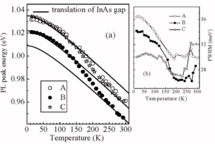
Figure1共b兲shows PL spectra of three DWELL samples measured at 14 K. Fitted by two Gaussians, the full width at half maximum 共FWHM兲 values for the main peak of three samples A, B, and C are 36.8, 34.2, and 30.0 meV, respec-tively. These FWHM values are small in comparison with recent results,8indicating the high growth quality of our QD samples. At 14 K, the PL peak energy of sample B is 1.0208 eV, which is smaller than those of samples A 共1.0320 eV兲 and C 共1.0344 eV兲. The PL peak energy is very dependent on growth conditions. A redshift of PL peak is observed from samples A and C to sample B, which can be attributed to the multilayer growth and an increase of InAs layer thickness. Sufficient stress release for the upper layer QDs can appear within the multilayer QD structure, leading to a decrease of the QD emission energy.9 This also causes the broadening of QD PL emissions,9leading to a larger PL FWHM of samples A and B than sample C. Further, larger QD size due to an increase of InAs QD layer thickness may also generate longer wavelength PL emissions.
Figure2 exhibits T-dependent PL spectra for samples A and B in 14– 300 K共some shown only兲. An obvious PL red-shift and a reduction in PL intensity can be observed as T increases. It is seen that PL spectra at every T can be fitted by two Gaussians. All PL spectra in Fig.2consist of two peaks, labeled by peak 1 for the lower energy and peak 2 for the higher one. Peak 1 is the main PL peak for all cases, due to emissions from QDs. Peak 2 has a weaker emission, related to the InGaAs strain layer in the DWELL structure, whereas dots grown on GaAs and covered with InGaAs present a more symmetric PL line shape.10
Different from single-layer InAs QDs, for the equal thickness of every period, the strain transition effect of multilayer structure induces an effect to influence the size of self-aligned QDs, having the QDs at the upper layer with larger sizes. In addition, there exist some no-self-aligned QDs usually with smaller sizes. These two factors cause a distribution of QD sizes, formatting both larger and smaller size QDs. From the self-aligned effect of larger size QDs, the number of larger size QDs is much more than smaller ones and the PL intensity of larger size QDs is much stronger.
The emission wavelength from the In共Ga兲As QDs on GaAs is typically around 1.0m at room temperature 共RT兲.11
PL peak wavelengths of our three DWELL samples at RT are around 1.3m, which are longer than that of com-mon QDs directly grown on GaAs matrix, and more suitable for optical fiber communication applications. This is due to the DWELL structure with InAs/ InGaAs QDs in a QW. The lattice constant of InGaAs is very close to that of InAs, which may result in stress release among InAs QDs, leading to the formation of large InAs QDs. It can narrow the band gap of InAs QDs and lead to a redshift of PL emissions. In addition, the energy sublevel overlap between quantum wells and dots may increase the carrier density in QDs,12and it is experimentally observed that multilayer structures with DWELL can greatly increase the QD PL intensity.5
Figure 3 exhibits the relationships of PL energy and FWHM of the main peak with temperature. All three DWELL samples show an anomalous redshift of PL peak energy with increasing T within 14– 300 K. At low T 共⬍150 K兲, sample C has the least FWHM value, and sample A has the largest one. However, FWHM values of samples A and B gradually decrease as T⬎150 K. Finally, the FWHM of sample B reaches the smallest one of 26.2 meV at ⬃240 K, and on the contrary, that of sample C comes to the largest one at T of ⬃270 K. These reveal a fact that in the multilayer DWELL structure, the carrier migration intensifies with T among different QD layers through the thin wall layer. In contrast, the migration is very weak when the wall layer is up to 50 nm, which results in a little change of PL FWHM with T. Therefore, these results indicate the enhance-ment of carrier migration among different QDs of DWELL samples in this T range.
FIG. 2. Temperature dependent PL spectra for samples A and B. FIG. 3. PL energy and FWHM of the main peak vs temperature.
126101-2 Kong et al. J. Appl. Phys. 101, 126101共2007兲
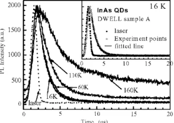
TRPL was measured for three InAs QD DWELL samples. Figure 4 shows TRPL spectra of sample A at sev-eral typical T and a typical decay curve fitting with a single exponential process for TRPL at 16 K. Figure5exhibits the relationship of PL peak lifetime versus T for three DWELL samples.
It is seen that at low T 共⬍50 K兲, the PL peak lifetime varies little with T, indicating the weak carrier migration among different QDs, which is same as PL characteristics of a single QD. PL lifetimes of all three samples increase as T rises from 50 to⬃150 K, which can be attributed to different mechanisms such as the thermally induced population of dark excitons and thermally induced carrier redistribution among QDs. We consider that the rate of carriers from GaAs or InGaAs QW layer to QDs decreases for scattering as T rises, which favors the increase of PL lifetime. As T moves beyond 50 K, the overall variation of PL peak lifetime from both samples B and C is larger than that of sample A, which may be related to the increase of density and size of QDs due to an increase of the InAs layer thickness. For larger QD diameters, electron and hole wave functions expand in dif-ferent directions and become more elongated, hence reduc-ing the overlap wave function and resultreduc-ing in a longer life-time. Multi-QW共MQW兲 structures may increase QD exciton
oscillator strength and decrease radiative lifetime, so sample C has a larger PL peak lifetime than samples A and B.
A significant variation appears at ⬃150 K, beyond which PL lifetime decreases 共until RT兲. It can casually be attributed to the thermal activation of nonradiative processes. Compared with QDs directly grown on GaAs matrix or In-GaAs strained layer, the InAs QDs grown in an InIn-GaAs quantum well exhibit a slight overall variation of PL lifetime 共1.2, 1.7, and 1.9 ns for samples A, B, and C, respectively兲, corresponding to PL characteristics, which shows that the DWELL structures have a better stability on temperature than the QDs not grown inside a QW.
In summary, we have shown that by using the structure of InAs QDs in an InGaAs/ GaAs quantum well on GaAs substrate, long wavelength emission near 1.3m can be achieved. Our results predicte that the close lattice constant of InGaAs to that of InAs may result in stress release among InAs QDs and large sizes of InAs QDs, which greatly im-proves the QD quality, narrows the band gap of InAs QDs, and leads to the redshift of PL emissions. In addition, the energy sublevel overlap between quantum wells and dots may increase the carrier density in QDs. It is found that in the multilayer DWELL structure, the carrier migration inten-sifies with temperature among different QD layers through the thin wall layer, resulting in a large decrease of PL FWHM with T. Compared with the InAs QDs directly grown on GaAs matrix or InGaAs strained layer with InAs QDs, the InAs QDs grown in an InGaAs quantum well exhibit a slight overall variation of PL lifetime. Our results provide good evidence of the stability on temperature from DWELL struc-tures.
We acknowledge the support of Dr. Zhichuan Niu and help from Nola Li. This work was supported partially by the Science and Technology Project of Zhoushan City, Grant No. 06110, and National Taiwan University by funds of NSC 94-2215-E-002-019 and NSC 95-2221-E-002-118.
1J. Ibáñez et al., J. Appl. Phys. 99, 043501共2006兲.
2J. H. Lee, Z. M. Wang, B. L. Liang, K. A. Sablon, N. W. Strom, and G. L. Salamo, Semicond. Sci. Technol. 21, 1547共2006兲.
3N. K. Cho, S. P. Ryu, J. D. Song, W. J. Choi, J. I. Lee, and H. Jeon, Appl. Phys. Lett. 88, 133104共2006兲.
4D. Bimberg, M. Grundmann, and N. N. Ledentsov, Quantum Dot
Hetero-structures共Wiley, New York, 1999兲.
5G. T. Liu, A. Stintz, H. Li, T. C. Newell, A. L. Gray, P. M. Varangis, K. J. Malloy, and L. F. Lester, IEEE J. Quantum Electron. 36, 1272共2000兲. 6A. I. Tartakovskii, R. S. Kolodka, H. Y. Liu, M. A. Migliorato, M.
Hop-kinson, M. N. Makhonin, D. J. Mowbray, and M. S. Skolnick, Appl. Phys. Lett. 88, 131115共2006兲.
7M. A. Cusack, P. R. Briddon, and M. Jaros, Phys. Rev. B 54, R2300 共1996兲.
8Yu. I. Mazur, B. L. Liang, Zh. M. Wang, D. Guzun, G. J. Salamo, Z. Ya. Zhuchenko, and G. G. Tarasov, Appl. Phys. Lett. 89, 151914共2006兲. 9H. Saito, K. Nishi, and S. Sugou, Appl. Phys. Lett. 73, 2742共1998兲. 10A. Fiore, P. Borri, W. Langbein, J. M. Hvam, U. Oesterle, R. Houdré, R. P.
Stanley, and M. Ilegems, Appl. Phys. Lett. 76, 3430共2000兲.
11C. Annalisa, C. Luciana, L. Gavriella, and V. Sesto, J. Cryst. Growth 261, 458共2004兲.
12F. Pulizzi, A. J. Kent, A. Patanè, L. Eaves, and M. Henini, Appl. Phys. Lett. 84, 3046共2004兲.
FIG. 4. Time-resolved PL spectra at several T for DWELL sample A and decay curve fitting共insert兲 for a TRPL spectrum measured at 16 K.
FIG. 5. Lifetime vs T for three DWELL samples A, B, and C.
126101-3 Kong et al. J. Appl. Phys. 101, 126101共2007兲