行政院國家科學委員會專題研究計畫 成果報告
高靈敏度 DNA 檢測系統之研究與開發(2/2)
研究成果報告(完整版)
計 畫 類 別 : 個別型 計 畫 編 號 : NSC 95-2221-E-002-216- 執 行 期 間 : 95 年 08 月 01 日至 96 年 07 月 31 日 執 行 單 位 : 國立臺灣大學機械工程學系暨研究所 計 畫 主 持 人 : 陳炳煇 計畫參與人員: 博士班研究生-兼任助理:錢睿宏、楊証皓 碩士班研究生-兼任助理:黃煒婷 處 理 方 式 : 本計畫可公開查詢中 華 民 國 96 年 09 月 21 日
行政院國家科學委員會補助專題研究計畫
■ 成 果 報 告
□期中進度報告
高靈敏度 DNA 檢測系統之研究與開發
Development of ultra high sensitive DNA detection system
計畫類別:■ 個別型計畫
□ 整合型計畫
計畫編號:NSC
95-2221-E-002-216
執行期間:
95 年
8 月
1 日至
96 年
7 月 31 日
計畫主持人:陳炳煇教授
共同主持人:
計畫參與人員:錢睿宏、楊証皓、黃煒婷
成果報告類型(依經費核定清單規定繳交):□精簡報告
■完整報告
本成果報告包括以下應繳交之附件:
□赴國外出差或研習心得報告一份
□赴大陸地區出差或研習心得報告一份
□出席國際學術會議心得報告及發表之論文各一份
□國際合作研究計畫國外研究報告書一份
處理方式:除產學合作研究計畫、提升產業技術及人才培育研究計畫、列
管計畫及下列情形者外,得立即公開查詢
□涉及專利或其他智慧財產權,□一年□二年後可公開查詢
執行單位:國立台灣大學機械工程學系
中
華
民
國
96
年
9
月
20
日
高靈敏度 DNA 檢測系統之研究與開發
Development of ultra high sensitive DNA detection system
計畫編號:NSC 95-2221-E-002-216 執行期限:95 年 8 月 1 日至 96 年 7 月 31 日 主持人:陳炳煇 國立台灣大學機械工程學系 計畫參與人員:錢睿宏、楊証皓、黃煒婷 國立台灣大學機械工程學系 ㄧ. 摘要 本計畫研究的目的,除了希望能利用現有專業晶圓代工技術如台積電、聯電所提供之標準 CMOS製程,配合MEMS 後製程處理來製作並開發具有量產能力的生物晶片檢測法。更希望 藉由奈米金粒子、奈米磁球、與DNA 之自組裝技術及生物條碼核酸偵測技術(bio-bar code DNA detection technique),來大幅提高檢測的靈敏度 (0.01fM)。並同時將積體電路、微型幫浦、 試液槽及流道整合成一小型檢測系統-μTAS(Micro Total Analysis System)。在本計畫中,新的 突破與創意就是利用奈米磁球、及生物條碼單股核酸偵測技術(bio-bar code ssDNA detection technique),來放大被檢測目標DNA 的數目,並利用此放大後DNA 的數目建立多層奈米金結 構,讓通過此奈米電極間多層奈米金結構的電流可以被簡單的儀器如三用電表等測得。
Abstract
The aim of this study is to develop an ultra high sensitive (0.01 fM) DNA detection system that is composed of standard CMOS IC fabrication, a DNA self-assembly technique, a bio-bar-code DNA detection technique, and a micro fluid system. This micro fluidic system has a micropump, microchannels, and reservoirs. The novelty of this proposal is to apply the magnetic nanoparticles and bar-code ssDNA(single strand DNA) to amplify the obtainable current through nanogap electrodes from the low concentration of target DNA. In this way, we can integrate the DNA detection technique, temperature control and sensing system, and the electrical detection circuit on a chip. Then, we can reduce the cost for fabricating the biochip. Furthermore, we will integrate a fully developing micropump technique into this detection system to realize the ideal of µTAS (Micro Total Analysis System) and to reduce the instrument space, production cost, and detection time, creating a portable biomedical detection instrument.
Keywords: CMOS biochip, DNA self-assembly technique, bio-bar-code DNA detection technique.
二. 目的與緣由
Principals
Fig.1 shows the layout of the circuits and Fig. 2 shows the current mirrors of the CMOS chip. One cascode current mirror is composed of four MOSFETs. The amplification factor of one cascode current mirror depends only on the ratio of W /L, where W and L denote the width and the length of the channel of MOSFET, respectively. After considering the range of input current signal, iD1, and
the range of load resistor, Rload, the amplification factor for each cascode current mirror is chosen as:
where iD is the current flowing through MOSFET from source to drain, the subscript 1 and 2
denote the input and amplified currents, respectively. After performing five stages of amplification,
iD3/iD1= 105 is obtained, where iD1is the input current signal from the detection electrodes and iD3
is the output current signal for measurements.
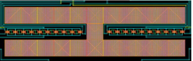
Fig. 1. The layout of the sensing circuits.
Fig.2 the schematic diagram of the circuits.
Determination of specific DNA sequences in biological samples can detect and identify certain infectious or inherited diseases or identify specific species. The purpose of DNA biochips development is to achieve rapid and reliable detection of specific DNA sequences from individual specific genes. Recently, with the rapid progress of modern technologies, especially nanotechnology, biotechnology and microelectronics, novel medical instruments have been proposed extensively.[1-4] There is a trend to develop more immediate and inexpensive diagnostic devices. Thus, the development of an accurate, portable and relatively inexpensive biosensor has become one of the most important issues in the healthcare industry. The introduction of complementary metal oxide semiconductor (CMOS) chips for DNA identification may overcome traditional problems and satisfy the requirements for inexpensive, accurate, and rapid detection because the fabrication processes for CMOS biochips are so mature that the detection circuit for CMOS biochips can be less than 1 μm.Many CMOS orCMOS-process compatible biochips have been introduced using two typical DNA detection methods, namely an optical approach and an electrochemical approach [5–9].
Taton et al. [10–12] presented a DNA detection method by UV absorption of multilayered gold nanoparticles on a glass substrate. The detected signal can be amplified by the growth of gold nanoparticles through a chemical reduction of silver in the sample solution. The sensitivity of this detection method exceeds that of conventional fluorescence detection methods by two orders of
magnitude in DNA identification. The same research group reported another novel DNA electrical detection method in 2002 [13]. They utilized the binding of oligonucleotide-functionalized gold nanoparticles in a 20 μm gap between two electrodesto vary theimpedanceofthegap,and used a silver enhanced solution to amplify the originally undetectable signal. Tsai et al. [14] presented an electrical detection method that, instead of silver enhancement, made use of multilayer self-assembled gold nanoparticles for signal amplification between nanogap electrodes. The same group used a standard CMOS process to fabricate a DNA biochip for electrical detection of DNA in 2005 [15]. In the studies of Tsai's group [14,15], the detected electric current over multilayer gold nanoparticles through nanogap electrodes was at an order of nA when the concentration of the target DNA strand was low. Unfortunately, most detection methods mentioned above utilize expensive and complicated optical or electrical equipment, and are inconvenient for quick and inexpensive measurements.
In this study, cascode current mirrors are employed to amplify the low electric current, and a temperature system is used for single base-pair mismatch detection. The biochip is fabricated by a standard CMOS fabrication process combined with post-CMOS micromachining processes. The electrical detection method utilizing a self-assembly gold nanoparticle multilayer without silver enhancement is used to detect the hybridizations among probe, capture, and target oligonucleotides. Before taking DNA detection measurements, a self-assembly monolayer of AuNPs is established on a SiO2surface between two microelectrodes. Then, capture oligonucleotide strands are immobilized
on the top surface of the self-assembly monolayer of AuNPs. If target oligonucleotide strands are complementary with the probe and capture oligonucleotide strands in the solution, specific binding can occur among thiol-modified probe, capture, and target oligonucleotide strands. Finally, through a self-assembly process between suspended gold nanoparticles and the thiol-modified end of the probe oligonucleotide strand, multilayer AuNPs on the nanogap surface can be established. According to the method proposed by Tsai et al. [14], Fig. 3 illustrates the procedure to establish
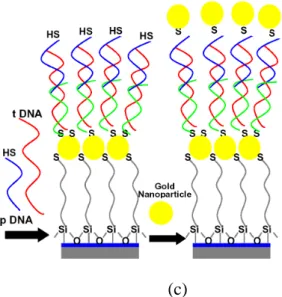
multilayer gold nanoparticles on the gap surface between two microelectrodes. With the integration of a current amplifier on the CMOS biochip, a commercial Volt-Ohm-Milliammeter can then be used for DNA identification. First, the single strand thiol-modified capture oligonucleotides (labeled as cDNA in Fig. 3(b)) is added to the nanogap and immobilized onto the surface of monolayer gold nanoparticles. Selective binding occurs among immobilized capture oligonucleotide strand, suspended probe oligonucleotide (labeled as pDNA in Fig. 3(c)), and target oligonucleotide strand (labeled as tDNA in Fig. 3) in the sample solution. One end of the probe oligonucleotide DNA is modified by thiol. Finally, the measured spot is rinsed with a PBS solution before adding gold nanoparticles. If there is no hybridization among the oligonucleotide strands, all the probe oligonucleotide and target oligonucleotide will be washed away. No gold nanoparticles would be attached to the capture oligonucleotide immobilized on the gold nanoparticle monolayer. However, if complementary hybridization occurs between oligonucleotide strands, gold nanoparticle probes can be attached to the thiol-modified probe oligonucleotide to form multilayer of gold nanoparticles for electrical detection.
(a)
Fig. 3. The chemical procedures for immobilization of the biomolecules.
When applied to base mismatch detection, hybridization assays are inherently limited in sensitivity. Detection of a point mutation in the test sequence (e.g., a small segment of genomic DNA) requires a distinguishable difference in pairing energies between a completely complementary and a mutated target strand. With only a single mutation in an extended oligonucleotide, the difference can be very small. In this detection system, temperature, or a thermal stringency wash, which is compatible with CMOS fabrication process, is the conventional tool for distinguishing single basepair (bp) mismatch.
On the other hand, the BCA method successfully demonstrates the feasibility of electrical detection to DNA biochip with MNPs and bio-bar-code DNA that give some results for the diagnostic biosensor for swift disease detection. Moreover, an electrical detection of DNA hybridization between the nanogap electrodes can be identified even in the lowest DNA concentrations. The development added a huge quantity of MMPs that has greater effect upon providing a powerful tool for detection of the reaction vessel to facilitate the binding DNA molecular.
Methods
Since the resistance of polysilicon increases with temperature, snack-like polysilicon layers in the standard CMOS process are used for heating and temperature sensing. Poly 1 layer and poly 2 layer beneath the microelectrode represent heaters and temperature sensors, respectively. Poly 1 (heater) is an applied voltage to generate heat to denature target DNA. After calibrating the relation between temperature and resistance of poly 2 (temperature sensor), we can monitor temperature change from the variation of resistance of poly 2. Due to thermal dynamic properties, the melting temperature measured from temperature sensors of single bp mismatch target DNA will be less than that of perfect match target DNA. The sequences of single strand capture, target, and probe DNAs ((C1DNA, T1DNA, and P1DNA) and (C2DNA, bar-code DNA, and P2DNA)) are shown in Table 1.
Nanometer size Fe3O4 particles were fabricated in this experiment and chemical
coprecipitation technique was used to synthesize fine ferromagnetic particles of iron ferrite. The first step in fabrication process was determination of the materials FeCl2, FeCl3, and NH4OH. Then
FeCl2and FeCl3solutions were weighed out 9.02 g FeCl2·4H2O and 3.32 g FeCl3·6H2O respectively.
After weighing the materials we added 34 ml of distilled water to each material and stirred them for Table 1. The sequences employed
15 minutes to make sure all the particles were dissolved in the solution. Then the three solutions were mixed in a beaker and stirred it for 30 minutes, at 500 rpm. Here, the aqueous 30 wt% solution NH4OH was added to the solution at a control pH value (10-11.8). After decantation, the
suspensions were heated at 80°C for 1 hour under continuous mixing and separated by centrifuging three times in distilled water so as to remove impurities.
The magnetic nanoparticles are approximately spherical and the average size was about 27 ± 4 nm according to the high-resolution transmission electronic microscope (HR-TEM, model: H-7000, Hitachi). Since preparation of AuNPs and fabrication of nanogap electrodes on silicon wafer are as those in our prior studies, one can find detailed procedures in those papers.
The procedure for electrical detection of bar-code DNA can be stated as follows. Here, the materials for DNA chip can be prepared two DNA components. First of all, 1ml MNPs was mixed with 2 ml of 0.3 M phosphate-buffered saline (PBS) buffer, and then added the first capture DNA (C1DNA) with the first target DNA (T1DNA) hybridization on MNPs. Four different concentrationsofT1DNA (1 nM,10 pM,100 fM,1fM)solution (50 μL )and C1DNA solution (50 μL,0.1 μM)can behybridizedwith in 24 hours at the room temperature, followed by using a 6000 Gausspermanentmagnetand 100 μL of0.3 M PBS bufferto separatesolid and liquid for 3 times. Moreover,thefirstprobeDNA (P1DNA)(100 μL,6 μM)and thesecond captureDNA (C2DNA) (100μL,6 μM)with bar-codeDNA (100 μL,6 μM)hybridization werein 100 μL of0.3 M PBS on AuNPs(100 μL).A 0.3 ml10% wt% BSA bufferwas added and incubated at 37℃ for 2 hours to stabilize the gold nanoparticles. After the above-mentioned, the C1DNA of MNP-DNA conjugate, P1DNA of AuNP-DNA conjugate, and T1DNA were hybridized. Furthermore, unbinding AuNP-DNA conjugate and MNP-DNA conjugate can be separated via a 6000 Gauss permanent magnet and 0.3 M PBS buffer for 3 times to wash. Finally, C2DNA and bar-code DNA of three-component MNP-DNA conjugate were denatured by washing with a 0.01 M PBS (0.01 M NaCl, 10 mM NaH2PO4/Na2HPO4, pH 7) buffer for 5 minutes at room temperature. By this method,
bar-code DNA can be collected and cooled in a refrigerator, immediately prior to use on-chip. The substrate was cleaned by immersion in 1:1 concentrated HCl:MeOH for 30 min, followed by rinsing with distilled water. The substrate was then immersed in concentrated H2SO4 for 5 minutes
and was rinsed with distilled water. There withal, it was immersed in the 1 mM 3-Aminopropyltrimethoxysilane (Sigma Chemical Co. St louis, MO) of DMSO solution for at least 2 hours at room temperature, followed by rinsing with DMSO and dried under N2. The
functionalized substrate was immersed in the AuNPs solution for 24 hours, then rinsed with distilled water and dried under N2.
The sequences of single strand capture, target, and probe DNAs ((C1DNA, T1DNA, and P1DNA) and (C2DNA, bar-code DNA, and P2DNA)) are shown in Figure 4 (b). Here, target DNA is bar-code DNA, owing to this study for the bio-bar-code amplification technique that can measure bar-code DNA rather than target DNA (T1DNA). In this study, bar-code DNA substitute for T1DNA
can be detected via AuNPs, MNPs, and DNA hybridization. The oligonucleotides were prepared according to standard protocols.
(b)
Fig.4 The procedure for bar-code DNA with magnetic nano-particles.
Except the middle layers, both bottom and top layers were established by using the same chemical compounds for the different procedures, APTMS for the bottom layer and DNA hybridization for the top layer. The middle layer was formed by using hexanedithiol as a linking chemical compound. It was worth noting that the number of middle layer can be greater than one. APTMS, whose thiol end was bound with gold nanoparticle, modifies silicon oxide substrate surface. To perform the detection of bar-codeDNA,C1DNA (100 μL,1 μM)was washed out in 10 mM HEPES (4-(2-hydroxyethyl)-1- piperazineethanesulfonic acid, J. T. Baker Chem. Co.), 5 mM EDTA buffer, pH 6.6 (HEPES buffer). The self-assembled gold-particle monolayer substrate was immersed in the C2DNA solution for 15 hours at room temperature, followed by rinsing with 50 mM sodium phosphate, 1 M NaCl, pH 6.5 (SPSC buffer) to remove non-covalently bound DNA, and was dried under N2. The substrate was immersed in four different concentrations of bar-code
DNA (1 nM, 10 pM, 100 fM, 1fM, 24-mer)solution (100 μL)and P2DNA solution (12-mer, 100 μL,0.1 μM)for2 hoursto hybridize,followed by immersing in aSPSC bufferto removeexcess reagents. The substrate was then immersed in a solution of AuNPs in 0.3 M PBS buffer (0.3 M NaCl, 10 mM NaH2PO4/Na2HPO4, pH 7), followed by washing with the 0.3 M PBS buffer to
remove excess AuNPs and was dried under N2. If hybridization among DNAs (P2DNA, C2DNA /
bar-code DNA) does occur, the top layer of gold nanoparticles is established between nanogap electrodes. If there is no hybridization, only monolayer of gold nanoparticles is established. However, a higher electrical current can be detected through self-assembly multilayer gold
nanoparticles if bar-code DNA, probe DNA, and nanoparticles are placed in the solution at the same time. When gold nanoparticles are placed in the solution after the hybridization between bar-code, probe, and capture DNAs, the electrical current is not as high. In this study, the later approach for establishing self-assembly gold nanoparitcle mutlilayer is used.
三. 完成結果與實驗討論
Fig. 5 shows the completed CMOS biochip. Since dry etching gas exhibits high selectivity between aluminum and SiO2, the metal layers can be used as an etching mask. Due to anisotropic
etching of SiO2 by RIE, the pattern of microelectrodes is formed defined by the layers of metal 2
and via 1. Microelectrodes lie on the layer of metal 1. The reaction ion etching continues until the microelectrodes appear. The surface of the nanogap between microelectrodes is still made of SiO2
for DNA immobilization.
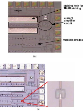
Fig.5 The results of the post CMOS process procedures.
Fig. 5(a) and (b) illustrate the micrograph of the CMOS biochip before and after post-micromachining process, respectively. This chip is fabricated by TSMC 0.35 μm 2P4M standard CMOS process, with a dimension of 1 mm × 3 mm, and there are 80 measuring spots on the biochip. The nanogap is 350 nm in width, 5 μm in length,and 2μm in thickness.
Fig.6 The SEM of the nanoelectrodes. (a) single layer, (b) double layer.
Fig. 6(a) and (b) show the FE-SEM micrographs of gold nanoparticle monolayer and multilayer immobilized in the gap between two microelectrodes, respectively. The white spots in the micrographs are gold nanoparticles. The distribution density of gold nanoparticles of the multilayer is much larger than that of the monolayer. It can be observed that the gold nanoparticles are discretely scattered and not continuously distributed on the gap.
(a)
(b)
Fig.7 The I-V curves of the measurement results. (a) single layer of AuNPs, (b) double layer of AuNPs.
Fig. 7(a) and (b) show the I –V characteristic curves of the monolayer and multilayer gold
nanoparticle structure over a 350 nm gap without current amplifier circuit, respectively. In this study, we use the semiconductor device analysis system (HP 4156) to measure the electrical signals. The noise level of this machine is about several fA and the scanning rate for the I –V curve measurement
is 10 mV/s. After successful immobilization of the gold nanoparticle monolayer on the gap, the electric current passing through the two microelectrodes is lower than 10 pA ( Fig. 7 (a)) with an applied voltage of 1 V. Although gold nanoparticles do not contact directly with each other, the current passing through the microelectrodes is still detectable. It is assumed to be the result of the tunneling effect through isolated gold nanoparticles. The measured I –V curve for the gold
nanoparticle monolayer follows the Ohm's law with some fluctuations. After hybridization among oligonucleotide strands over the gold nanoparticle monolayer, the electric current passing through two microelectrodes for the multilayer of self-assembly gold nanoparticle increases to a value of 10 nA at an applied voltage of 1 V ( Fig. 7 (b)). It is noted that the concentration of target oligonucleotides in the sample solution is 10 nM.
In order to decrease the total detection time and simplify the operation steps of the integrated microfluidic device, we have to proceed some experimental procedures in preparation step.
Firstly, a self-assembly gold nanoparticle monolayer is immobilized in the gap by carbon strains after a nanogap is fabricated between two microelectrodes.
inlet outlet reaction chamber silicon rubber
Fig.8 The photos of the micro total analyzer.
The integrated microfluidic device includes two parts: one is a glass substrate where the CMOS biochip was bonded and the other is a PDMS microfluidic chip, shown in Fig. 8. Elastic PDMS was used to duplicate microchannels from a mold with reverse fluidic structures and thin films. After the bonding of CMOS biochip and PDMS chip, the whole DNA detection system can then be portable and the ability of automation can be also increased. The detail descriptions of the integration and
(a)
detection process are as follows.
Finally, the measured spot is rinsed with a PBS solution before adding gold nanoparticles. If there is no hybridization among the oligonucleotide strands, all the probe oligonucleotide and target oligonucleotide will be washed away. No gold nanoparticles would be attached to the capture oligonucleotide immobilized on the gold nanoparticle monolayer. However, if complementary hybridization occurs between oligonucleotide strands, gold nanoparticle probes can be attached to the thiol-modified probe oligonucleotide to form multilayer of gold nanoparticles for electrical detection. Fig. 8 (b) is the photograph of the whole experimental setup of the integrated microfluidic device. Syringe pump (KDS, 101) is used to pump fluids in microchannel of this microfluidic chip.
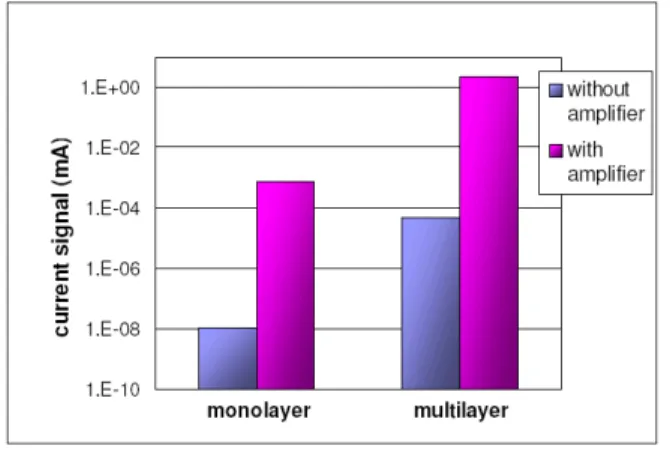
Fig.9 the comparison of the measurements.
Fig. 9 illustrates the comparison of the current signals of the monolayer and multilayer gold nanoparticle structure over a 350 nm nanogap with and without the current amplifier circuit. The electric signal (mA) of the multilayer gold nanoparticle structure over the nanogap could be detected by a commercial Volt-ohm-Milliammeter. After combining the microelectrodes with the current amplifier circuit, the current signals of the monolayer and multilayer gold nanoparticle structure are successfully amplified to the level of 1 μA and 1mA, respectively.
Fig. 10 The curve fitting of the resistance with temperature.
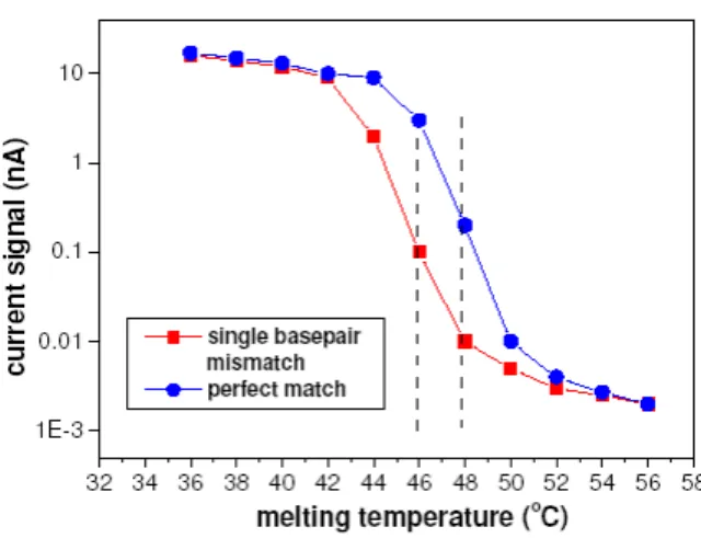
The current mirrors play a key role in the CMOS biochip.In the temperature system, the calibration curve of the relation between temperature and resistance of poly 2 (temperature sensor) is shown in Fig. 10. The resistance of poly-silicon increases quite linearly with temperature. Fig. 10 illustrates current signals versus melting temperatures of single bp mismatch and that of perfect match of target DNA that can be distinguished by the 2 °C difference in melting temperature. The current signal of perfect match target DNA decreases dramatically at 48 °C, but that of single bp mismatch target DNA occurs at 46 °C. From this result shown in Fig. 11, we can find out single mutation of target DNA precisely.
Fig. 11 The comparison of the measurement of single basepair mismatch and complimentary nucleic acids.
For identifying the specificity of bar-code DNA, it is required to check whether the hybridization among DNAs has any mismatch. To check it, the chip is washed with a 0.01 M PBS buffer at room
temperature. If the hybridization among DNAs is not fully complementary, the top layer of AuNPs is washed away. As a result, the electrical current is reduced significantly back to a value that is obtained for self-assembly gold nanoparticle monolayer. The measurable I-V curves of the array biochip are obtained from a HP 4156A precision semiconductor parameter analyzer in the voltage ranges from -1 to +1 V with a scan rate of 1 mV/s. The noise produced in regular electronic devices would render it impossible to detect the current signal at a pico-ampere level unless the signals can be amplified without noise interference. Usually, pico-ampere level electric signal can only be detected with some extremely sensitive instrument (e.g. HP 4156 Semiconductor Device Analysis System). In this study, the current mirrors have been effective in amplifying the signal through both the monolayer and multilayer gold nanoparticles, and thus have allowed us to obtain the current through multilayer gold nanoparticles with a common commercial Volt-ohm-Milliammeter.
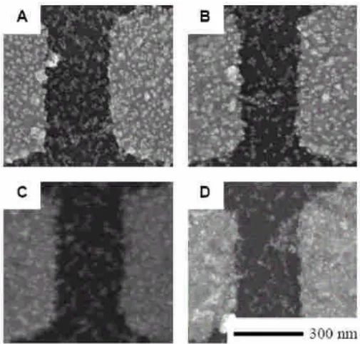
The 1 fM to100 fM T1DNA measurement with and without BCA shows the different results in Fig. 12. The FE-SEM images show the particles distribution different from with and without using BCA method. The BCA procedure described above provides a versatile and distinct I-V curve for DNA detection.
Fig. 12. The FE-SEM of the different concentrations of targets (A) 1 nM, (B) 10 pM, (C) 100 fM, and (D) 1 fM.
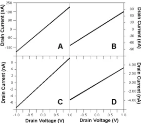
Current-voltage (I-V) behavior of the devices is measured as shown in Fig. 13. The larger concentration of T1DNA would make the larger current. In these figures, the I-V curves show the
current of the electrode, and the conductance ( I / V ) of the different-concentration T1DNA are ~ 2.2 × 10⁻⁴ s, ~ 7.5 × 10⁻⁸ s, ~ 7.8 × 10⁻⁹ s and ~ 3.6 × 10⁻⁹ s. The lowest values of the T1DNA
concentration indicate the lowest conductance.
Fig. 13 The I-V curve of the different concentrations of the target DNA (A) 1 nM, (B) 10 pM, (C) 100 fM, and (D) 1 fM.
Conclusion
In this study, a DNA detection system including DNA biosensors, a current amplifier circuit, and a temperature system for single basepair mismatch detection is designed and developed for DNA identification by electrical detection. A novel technique using a self-assembly method combined with cascode current mirrors to amplify electrical signals is presented.
The electric current passing through the gold nanoparticle multilayer, which is formed by complementary target oligonucleotide strands, exceeds that through the gold nanoparticle monolayer by three orders of magnitude. After being amplified by the current mirrors, the electrical signals of the multilayer gold nanoparticle structure over a nanogap can be measured by a commercial Volt-ohm-Milliammeter. With temperature sensors and heaters, single mutation of target DNA could be distinguished precisely. We have demonstrated that the combination of CMOS biosensor structures, IC design technique and commercially available electronic devices is useful to identify
specific DNA sequences. CMOS process, which is widely applied to digital and analog IC, is very common and standard in the semiconductor industry. This means that CMOS based instruments by mass production can be of relatively low cost for the healthcare industry. The characteristics of CMOS chips make this device very attractive to be developed as personalized clinical diagnostic instruments.
The BCA method mentioned in the previous section is implemented. In this study, the analysis successfully demonstrate the feasibility of electrical detection to DNA biochip with MNPs and bio-bar-code DNA that give some results for the diagnostic biosensor for swift disease detection. Moreover, an electrical detection of DNA hybridization between the nanogap electrodes can be identified even in the lowest DNA concentrations. Significantly, concepts for the electrical detection of nanostructural differences in DNA sequences that can be easily manipulate the magnetically labeled target DNA. Therefore, the development added a huge quantity of MMPs that has greater effect upon providing a powerful tool for detection of the reaction vessel to facilitate the binding DNA molecular. The interrelated application for the biological samples of DNA biochip with BCA method to improve the commercial potential of the novel biochip platform is foreseen.
Measurable current through nanogap electrodes can be obtained over multilayer gold nanoparticles. In this way, magnetic nanoparticles and bio-bar-code DNA are used to amplify obtainable current through nanogap electrodes from the extremely low concentration of target DNA. The detective concentration of target DNA with electrical DNA biosensor is as low as 1 fM for the analysis of current-voltage curves.
四. 計畫成果自評
The targets achieved are listed as the follows,
1. Detection limit of developed CMOS DNA biochip is 10pM.
2. The electric current passing through the multilayer AuNP, which is formed by complementary target DNA, exceeds that through the monolayer AuNP by three orders of magnitude. After being amplified by the current mirrors, the electrical signal of the multilayer gold nanoparticle structure over a nanogap is successfully amplified to the level of mA and can then be measured by a commercial Volt-ohm-Milliammeter.
3. With temperature sensors and heaters, single mutation of target DNA could be distinguished by about 2oC difference in melting temperature for the tested target DNA with a length of 27 bp.
4. A good agreement is found between measured and simulated surface temperature of nanogap on the CMOS biochip if the heater is powered with a given voltage.
5. DNA detection can be performed on either the developed CMOS biochip alone or on the developed CMOS biochip integrated with microfluidic device.
6. The BCA technique measures the bar-code DNA rather than the target DNA. The DNA chips with nanogap electrodes are fabricated by Electron-beam lithography. The gap distance and an electrode height are 300 nm and 65 nm, respectively. Here, the surface between electrodes and multilayer of gold nanoparticles is established by the hybridization among single strand BCA, the second capture DNA (C2DNA) and the second probe DNA (P2DNA).
成果列表: 預期完成之工 作項目 執行情形 差異性 1. 奈米電極 經由量測電阻值,辨識原本未接通之電極間 隙,已由DNA 與奈米金微粒所組成的電橋而導 通。 無差異 2. 電訊號放大電路 將電流訊號放大至毫安培等級,以利後續電訊 號處理及偵測。 無差異 3. Bar-Code 磁球放大訊號 之功能 靈敏度足以媲美PCR 技術;甚至還可以檢測 出單一鹼基錯配(single-base mismatches)的情形 無差異 4. 微流體系統方面 流體驅動元件整合完成將CMOS晶片整合,並 接線以量測電訊號。 無差異 五. 發表文獻 本計畫目前為止完成之結果已有二篇獲得國際知名期刊接受,並有兩篇獲得國際研討會接 受口頭發表研究成果。
Detection Biochip,”Sensors and Actuators B: Chemical. (IF= 2.083)
2. T. L. Chang, C. Y. Tsai, C. C. Sun, U. Ramesh, C. C. Chen, C. H. Lin, and P. H. Chen, 2006, “ElectricalDetection ofDNA Using Gold and MagneticNanoparticlesand Bio Bar-Code DNA between Nanogap Electrodes,”Microelectronic Engineering, (IF= 1.514)
3. Y. T. Cheng, C. Y. Tsai, and P. H. Chen,“A CMOS Biochip forElectricalDetection ofDNA with an Embedded CurrentAmplifierCircuit”,IEEE-NEMS 2006, Zuhai, China, 102.
4. J. H. Chien,Y.T.Cheng,P.Y.Wang,and P.H.Chen,“A RFID Tag Based RemoteDNA sensing System”,IEEE-NEMS 2006, Zuhai, China, 101.
六、參考文獻
[1] Swanson, P.; Gelbart, R.; Atlas, E.; Yang, L.; Grogan, T.; Butler, W.F.; Ackley, D.E.; Sheldon, E., "A fully multiplexed CMOS biochip for DNA analysis" Sens. Actuators B: Chem. 2000 pp. 22-30
[2] Yang, J.M.; Bell, J.; Huang, Y.; Tirado, M.; Thomas, D.; Forster, A.H.; Haigis, R.W.; Swanson, P.D.; Wallace, R.B.; Martinsons, B.; Krihak, M., "An integrated, stacked microlaboratory for biological agent detection with DNA and immunoassays" Biosens. Bioelectron. 2002 pp. 605-618
[3] Lobert, P.E.; Bourgeois, D.; Pampin, R.; Akheyar, A.; Hagelsieb, L.M.; Flandre, D.; Remacle, J., "Immobilization of DNA on CMOS compatible materials" Sens. Actuators B: Chem. 2003 pp. 90-97
[4] Chen, J.H.; Chen, T.F.; Huang, R.S.; Gong, J.; Li, J.C.; Chen, W.C.; Hseu, T.H.; Hsu, I.C., "A novel micro-well array chip for liquid phase biomaterial processing and detection" Sens.
Actuators A: Phys. 2003 pp. 193-200
[5] Albers, J.; Grunwald, T.; Nebling, E.; Piechotta, G.; Hintsche, R., "Electrical biochip
technology—a tool for microarrays and continuous monitoring" Anal. Bioanal. Chem. 2003 pp. 521-527
[6] Li, J.; Xue, M.; Lu, Z.; Zhang, Z.K.; Feng, C.G.; Chan, M.S., "A high-density conduction-based micro-DNA identification array fabricated with a CMOS compatible process" IEEE Trans.
Electr. Dev. 2003 pp. 2165-2170
[7] Moreno-Hagelsieb, L.; Lobert, P.E.; Pampin, R.; Bourgeois, D.; Remacle, J.; Flandre, D., "Sensitive DNA electrical detection based on interdigitated Al/Al2O3microelectrodes" Sens.
Actuators B: Chem. 2004 pp. 269-274
[8] Guiducci, C.; Stagni, C.; Zuccheri, G.; Bogliolo, A.; Benini, L.; Samori, B.; Riccò, B., "DNA detection by integrable electronics" Biosens. Bioelectron. 2004 pp. 781-787
[9] Kim, D.S.; Jeong, Y.T.; Park, H.J.; Shin, J.K.; Choi, P.; Lee, J.H.; Lim, G., "An FET-type charge sensor for highly sensitive detection of DNA sequence" Biosens. Bioelectron. 2004 pp. 69-74
[10] Taton, T.A.; Mirkin, C.A.; Letsinger, R.L., "Scanometric DNA array detection with nanoparticle probes" Science 2000 pp. 1757-1760
[11] Taton, T.A.; Mucic, R.C.; Mirkin, C.A.; Letsinger, R.L., "The DNA-mediated formation of supramolecular nano- and multilayered nanoparticle structures" J. Am. Chem. Soc. 2000 pp. 6305-6306
[12] Taton, T.A.; Lu, G.; Mirkin, C.A., "Two-color labeling of oligonucleotide arrays via size-selective scattering of nanoparticle probes" J. Am. Chem. Soc. 2001 pp. 5164-5165
[13] Park, S.J.; Taton, T.A.; Mirkin, C.A., "Array-based electrical detection of DNA with nanoparticle probes" Science 2002 pp. 1503-1506
[14] Tsai, C.Y.; Tsai, Y.H.; Pun, C.C.; Chan, B.; Luh, T.Y.; Chen, C.C.; Ko, F.H.; Chen, P.J.; Chen, P.H., "Electrical detection of DNA hybridization with multilayer gold nanoparticles between nanogap electrodes" Microsyst. Technol. 2005 pp. 91-96
[15] Cheng, Y.T.; Pun, C.C.; Tsai, C.Y.; Chen, P.H., "An array-based CMOS biochip for electrical detection of DNA with multilayer self-assembly gold nanoparticles" Sens. Actuators B: Chem. 2005 pp. 249-255