Test Time Reduction in Scan Designed Circuits
Wen-Joung Lai, Chen-Pin Kung & Chen-Shang Lin
Department of
Electrical Engineering
National Taiwan Universil y
Taipei, Taiwan, R.O.C.
,4 b
s
t
ract
T h e reduction of t e s t application t i m e f o r t h e gener- al s c a n designed circuits had been studied. T h e reduc- t i o n p r o b l e m had been investigated f r o m three aspects: t h e t e s t generation, selective scan, and rearrangement
of s c a n path. T h e t w o phase testing strategy had been proposed t o employ s c a n only f o r t h e hard-to-detect faults. F o u r cases of selective scan had also been i-
dentified. Furthermore, a n ordering h e u r w t i c without layoplt constraint had been proposeded t o m a x i m i z e the reduction of unnecessary scans and hence t h e t e s t ap- plication t i m e . A p p l y i n g these reduction methods, t h e total t e s t clockrcycles c a n be reduced t o only 20% on average f o r ISCAS sequential benchmark circuits with partial scan.
1
Introduction
The progress of vary large scale integration(VLS1) technology has brought tremendous improvement in chip performance as well as gate density. The increas- ing complexity, however, renders the testing of a VLSI chip much more difficult. For large sequential circuits, the automatic test pattern generation (ATPG) is quite time consuming and the resultant fault coverage is of- ten unacceptably low. The remedy is naturally t o take into account the testability while designing a chip, i.e., the design for testability. The most popular approach in design for testability is the scan design such as full scan[l] and partial scan[2]. In the scan design, all or part offlip-flops(FFs) in a chip are interconnected into a scan chain during test mode so that all these scan flip-flops(SFFs) can be controlled/observed by scan- in/scan-out operations. As a result, the test genera- tion problem can be significantly reduced[4]. However, the test application time of a scan-designed circuit is in general lengthened because of the extensive scan operations to shift in the patterns and shift out the responses. The reduction of test application time for scan designed circuits is the main concern of this pa- per.
To reduce the scan operations in a scan designed circuit, a straightforward way is to increase the num- ber
of
parallel scan chains, with additional overhead in pins. Recently, novel approaches[5, 6, 71 have beentThis work was supported in part by the National Science
Council R.0 .C under Grant NSC 82-0404-E-002-167.
proposed to reduce test application time by rearrang- ing and modifying the scan path. These approaches are constrained by the given test sequence and do not exploit the benefit from test generation. Moreover, some[6, 71 even have relied on the pattern indepen- dence of the full-scan circuits, which in general does not hold in the partial-scan designed circuits.
In this paper, the reduction of test application time of general scan designed circuits is studied. The prob- lem is investigated from three aspects: the test gener- ation, selective scan, and rearrangement of scan path. It will be shown in our experimental result that by al- lowing arbitrarily ordering of scanned flip-flops in the partial scan chain, the test application time can be reduced to only 20% on average.
In the next section, the reduction methods for the test application time of scan designed circuits will be described. Then the evaluation results on the sequen- tial benchmark circuits will be provided. And finally the conclusion will be given.
2
Test Time Reduction
for
Scan De-
signed Circuits
In this section, our reduction method for the test application time of scan designed circuits will be de- scribed.
First we will introduce a measure of test applica- tion time. In a scan designed circuit, the content of the scanned flip-flops (SFFs) can be controlled and observed by serial shift operations of the scan chains. Let S be the number of scanned FFs, T the number
of test patterns, and
P
the number of scan chains. Then for each applied test pattern, S I P shift oper-ations plus one actual testing operation are required. The response to be shifted out can be overlapped with the scan-in of the next pattern. Assuming that both shift operation and testing operation take the same amount of time, say one clock cycle, then for each pattern, ( S I P
+
1) clock cycles are required and for Tpatterns, T * ( S / P + l ) + S / P where the last term S I P
is due to the response scan-out of the last pattern. De-
fine the above required clock-cycles as the total test clock-cycles (TTCs), i.e.,
TTCs = T
*
( S / P+
I )+
S / P .Without loss of generality, we assume that there is
Given a scan path, the test application time can be reduced by exploiting and eliminating unnecessary scan operations. The reduction can be achieved in the test generation, selective scan, and the arrangement of scan path. They will be briefly described in the sequel.
2.1 Two Phase Test Generation
The two phase test generation strategy is based on the observation that in most scan designed circuits, a majority of faults can be easily detected even without scan. To take advantage of the above observation for reducing scan, the testing of a circuit can be separated into two phases: in the first phase, the circuit is tested
as a scanless circuit, and only in the second phase is the scan path utilised. To accommodate this testing strategy, the test generation is also split into two phas-
es: the scanless phase for easy-to-detect faults and the scan phase for hard-to-detect faults.
One might suspect that by splitting into two phas- es, the the test application time would be adversely lengthened. It will be demonstrated later that, with careful consideration, the converse is true. Significan- t reduction in scan and test application time can be obtained with this simple two phase testing strategy.
The balance between these two phases can be deter- mined as follows. In a sequential ATPG, the limit of iterative time frames(F) can be set by users. A fault which can be test generated within
F is in phase 1,
otherwise it belongs t o phase 2. Clearly, too large anF would include many hard-to-detect faults in the first
phase and inevitably lengthen the test sequence. On the other hand, a small F could drive most faults t o the second phase and thus need more scan operations. Since the test cycles t o place a given fault in phase 1 is no more than F and in phase 2 is proportional to
(S
+
l ) , which is the test cycle number for each test pattern, we could restricted iterative time frames in phase 1 such that F<
K
*
S+ l), where K is a given of test patterns for each fault t o be detected in phase 2. The number K unfortunately can not be known a priori. However, in our experiment, it is found thatK = 2 consistently quite good result in all evaluated
cases. A slightly better result is obtained by simplyletting our ATPG determine when to abort a fault to phase 2.
It is also worth noting that the two phase testing strategy does not require any additional hardware, i.e., no overhead except that of an ordinary partial scan. 2.2 Selective Scan
The objective of shift operations in the scan design is t o control the scan elements and to observe the effect of the previous pattern. However, it is not always nec- essary to control and observe every scanned element in every test pattern. Certain bits in a given pattern may be don't-care and response bits provide detection information only occasionally[5]. This sparseness of information
in SFFs
can be further explored during the test generation.During the second phase of the test generation, we modify the ATPG such that it deliberately leaves the pseudo PIS (SFFs) in don't-care whenever possible. number. The implication o
I
K is the average numberFigure 1: Scan Facility
The results show that averagely less than 28% of the scanned FFs in a circuit are used for actual test ap- plying purpose, and less than 8% for actual response observing purpose.
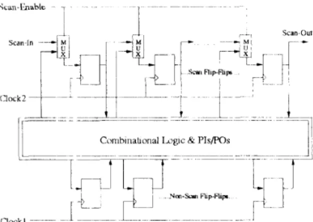
Based on the above observation, we are t o identify the unnecessary scan operations from a given test se- quence with sparse information and t o reduce the scan operations by selectively scanning. In the discussion, we assume that the scanned circuit has separate clock lines for the scanned flip-flops and the nonscanned flip- flops as shown in Figure 1. These two clock lines can be independently controlled to hold-data(disab1ed) or normal-operation(enab1ed) in each type of flip-flops. There is a n additional control line in the scanned cir- cuits, the Scan-Enable line, which enables the shift operation of the scanned flip-flops. The extra feature requires little overhead besides that required for scan design.
With these three control lines in a partial s-
canned circuit, the scanned flip-flops can be oper- ated as shift-register(S), hold-data(H), or normal- operation(N) and the unscanned flip-flops can be in normal-operation(
N)
or hold-data H). For example, and the shifting operation of the scan chain is in theSH mode.
Four cases of unnecessary scans are identified and methods of selective scan are devised to eliminate them.
the phase-one testing is performe
d
in the N N mode1. Actual Scan Requirement: The scan is only
performed to shift in all the effective test bats to the right position and l o shift out all the fault- effect response bits.
For a test pattern, the straightforward ( T T C s ) is
S
+
1, where S is the number of scan elements in the scan path. However, from test generation, it is possible to obtain the response bits ofTi
t o be shifted nut and the effective test bits ofT+l
t o be shifted in. The positions of these bits on the scan path allow us t o determine the number of actual scan requirement forz+l,
which is less than orI*- -
- s --4
scan-in
-4
XIXK
D S X T X ~ scan-outI
TI
Response bits Informarion
1
-- so--+T,+l scan-in
-
11x5
-1
:Tx$~-
scan-out T a t bits Informatioil: c---- SI --4
Figure 2: Actual Scan Requirement
equal to S. For example, in Figure 2, the number of shift of the pattern is M A X ( S O , S I ) , where
SO(S1) is the the maximum distance of the ef- fec tive response( test) bits from the scan-out(scan- in) pin.
This reduction method is supported by any par- tial scan designs. However, the reduction is heav- ily dependent on the ordering of scan elements.
2. Delayed Scan-Out: T h e scan-out operations
are n o t performed unless a fault-effect bit is in
danger of being overwritten by a n e w response.
As described earlier, the observation of fault effect
on SFFs only happens occasionally. Hence addi- tional scan reduction can be obtained if the rare fault effects can be held in the scan path so that their scan-out can be overlapped with the scan-in operations of the succeeding test patterns. For example, in Figure 2, if SO
>
SI and there is no SFF to be observed for the succeeding pattern- s such asx+l
and Ti+a, then only SI bits areshifted and the remaining fault effect bits of T, can be held in the scan path to overlap its shift- out with the scan-in operations of the succeeding patterns.
This reduction method requires the scanned flip- flops t o hold the scanning d a t a without being over-written by the new but useless responses. This ability is supported in our scan facility.
3. Reusable Scan-In: T h e scan-in operations are
performed only t o t h e point t h a t all effective t e s t bits are obtained.
In our scan facility, a bit in the scan path can be held without being over-written by the responses. This bit can be a fault effect as in the delayed scan-out. It can also be a scan-in test bit which can then be used in the succeeding patterns a t the farther positions of the scan path. For example, if
there is a
’1’at
thethird SFF of
the scan pathfor
T, and a single ’1’ is also needed a t the fifth SFF for T,+1, then only two shift operations between T, and
z+1
are required instead of the original five shift-operations. Therefore the scan numbercan be reduced. This reduction is possible only when
Ti
does not need t o observe any S F F and the original pattern is kept in the scan path by the hold operation.4. Concurrent Shift: If there is n o i m m e d i a t e
f a u l t effect t o be observed after applying a t e s t pattern, one shijl operation of t h e s c a n p a t h c a n operate concurrently w i t h t h e t e s t application of t h e circuit.
This concurrent shift utilizes the independen- t clocks of our scanned circuit, in which the s-
canned flipflops perform the scan-in operation of the next pattern while the unscanned flip-flops are loading the response. The concurrent shift is able to reduce at most one shift per pattern. The reduction is in general not significant but there is one advantage in the concurrent shift. Unlike previous cases, it is independent of the ordering of scan path.
2.3 Rearrangement
of
ScanPath
The effectiveness of most selective scan methods described above depend on the ordering of SFFs in the scan path. Here we consider the ordering problem with the assumption that all permutations of SFFs are feasible. In other words, no physical constraint on the ordering is considered in this paper. Howev-
er, we would like t o point out that, in our reordering procedure, it is possible to take the constraints into account.
The shift requirement of controlling/observing an
SFF directly depends on the position of this SFF in the scan path. An SFF placed close t o the scan-out pin will require approximately S shift operations t o set its value but only a few shifts can scan out its value for observation. On the other hand, a n SFF po- sitioned near the scan-in pin is significantly easier for scan-in. The ordering consequently must be a tradeoff of these two conflictive demands. Our heuristic is t o take as a weight the difference of a SFF’s controlling frequency and observing frequency obtained from test generation. And the ordering of the SFFs from the scan-in pin t o the scan-out pin is determined by the descending order of this weight.
By our experiments, this ordering of SFFs gives fairly good results for our reduction methods.
3
Results and
Discussion
ISCAS sequential benchmark circuits[3] are used to evaluate our reduction strategy. Each circuit is first partially scanned to attain a n acceptable fault cov- erage, then two-phase test generated, and finally se- lectively scanned with scan path rearrangement. The scanned flip-flops are selected based on a structural criteria[9] to achieve reasonable fault coverage. For the evaluated circuits, the performance of the selection criteria is comparable to that of [ll, 12, 131. The test pattern generator is a conventional propagate-then- justify generator and has performance comparable to
STG3[10].
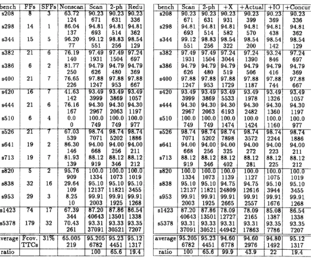
The evaluation result is shown in Table 1. In this table, “Nonscan” is the result of the original scanless
circuits, “Scan” the partial scan circuits with “SFF” FFs scanned, “2-Ph” the two-phase test generation, and “Redu” the final reduced result. For each case, the upper datum is the fault coverage and the lower datum is the TTCs (Total Test Clock-cycles).
We can see from Table 1 that the two-phase test generation alone reduces the TTCs t o 65.6% of the
conventional partial scan. This reduction is achieved with ordinary scan path and without any selective s-
can. Applying the selective scan techniques and the ordering of SFFs, the TTCs can be reduced t o 20%
averagely, which indicates a very significant reduction in the testing cost.
In Table 2, we show the cumulative effect of our test reduction methods. The column “2-Ph” is the same as Table 1, and “+X” is the result when delib-
erately leaving don’t-care on SFFs in the phase-two of test generation. Note that TCCs of “+X” are more than “2-Ph” because the ATPG’s heuristic of setting the unassigned PIS in phase-two is sacrificed for the benefit of the later selective scan. The column “+Ac- tual” is the actual shift requirement. And the column “+IO” is the result when further applying the delayed- scan-out and reusable-scan-in methods, while column “+Concur” the concurrent-shift method. The average efficiency of every reduction methods can be found in the last row of Table 2. Note that the increase of TCCs in “+X” is more than justified when subsequen- t selective scan is applied and TTCs are drastically
reduced. Most of our proposed methods, except con- current shift, provide significant reduction in TTCs.
Since the concurrent-shift at best can save one clock- cycle for every pattern, its effectiveness is not so good
as the other methods. On average, 80% total test clock-cycles reduction is achieved without restriction on the S F F ordering.
One might notice that the final fault coverage is slightly different from the original “Scan”. This is be- cause the modified ATPG sacrifice the heuristics for setting the unsigned SPIs and some faults are not de- tected without these heuristics. But for the circuit S5378, the fault coverage after test reduction become higher. This may due t o that in the scan reduction, values are assigned t o the unassigned SFFs during test generation and hence unintentionally detect some pre- viously undetected faults
4
Conclusion
The reduction of test application time in scan- designed circuits had been considered in this paper. The reduction problem had been investigated from three aspects: the test generation, selective scan, and rearrangement of scan path. The two phase testing strategy had been proposed t o employ scan only for the hard-to-detect faults. Four cases of selective s-
can had also been identified. Furthermore, a n order- ing heuristic without layout constraint had been pro- poseded t o maximise the reduction of unnecessary s-
cans and hence the test application time. Applying these reduction met hods
,
the total test clock-c ycles can be reduced t o only 20% on average forISCAS
se- quential benchmark circuits with partial scan.Although the evaluation had been performed for
the partial scan case with single path, we like to point out that all our discussions are also applicable t o other scan designed circuits.
References
E.B. Eichelberger and and T.W. Williams, “A Logic Ilesign Structure for LSI Testability,” J. Design Automa. Proc. Fault-Tolerant Comput., pp.165- 178, May 1978.
E. Trischler, !‘Incomplete Scan :Path with an Automatic Test Generation Methodology,” Proc. ITC, pp.153-162, Nov. 1980.
F. Brglez, D. Bryan and K. Kozminski, “Com- binational Profiles of Sequential Benchmark Cir- cuits,” Proc. ISCAS, pp.1929-1934, May 1989. S. Bhawmik, C.J. Lin, K.-T. Cheng and V.D. Agrawal, “PASCANT: A Partial Scan and Test Generation System,” Proc. CICC, pp.17.3.1- 17.3.4, 1991.
S.P. Morley and R.A. Marlett, “Selectable Length Partial Scan: A Method t o Reduce Vector Length,” Proc. ITC, pp.385-392, 1991.
S . Osstdijk, F. Beenker and L. Thijssen, “A Mod- el for Test-Time Reduction of Scan Testable Cir- cuits,” Proc. ETC, pp.243-252, 1991.
R. Gupta and M.A. Breuer, “Ordering Storage Elements in a Single Scan Chain,” Proc. ICCAD, pp.408-411, 1991.
J.-D. Pan, “Sequential Test Pattern Generation,” Master Thesis, National Taiwan University, 1991. W. Lai and C. Lin, “Selection of Scan Flip-FLps in Partial Scan Design”, Proc. 3rd VLSI/CAD Workshop, pp. 11-18, 1992.
W. T. Cheng and S. Davidson,”Sequential Cir- cuit Test Generation Benchmark Result” Proc. ISCAS, pp. 1931-1934, 1989
K. S. Kim and C. R. Kime, “Partial Scan by Use of Empirical Testability”, Proc. ICCAD, pp. 3 1 4 317, 1990.
K. T . Cheng and V. D. Agrawal, “An Economi- cal Scan Design for Sequential Logic Test Gener- ation”, Proc. FTCS, pp. 28-35, 1989.
D. H. Lee and S. M. Reddy, “On Determining S- can Flp-Flops in Partial Scan Design”, Proc. IC- CAD, pp. 322-325, 1990
Table 1: Results of Test Reduction l!Fs 8 14 15 21 6 2 21 16 21 6 4 21 19 19
Table 2: Accumulative Effect of Reduction Techniques