Characteristics of
Poly-Si Nanowire Transistors with Multiple-Gate Configurations
Hsing-HuiHSUa, Horng-ChihLina,b,*
,Ko-HuiLeea,Jian-FuHuangaand Tiao-YuanHuangaInstituteofElectronics, National ChiaoTungUniversity,No.1001, TaHsueh Rd., Hsinchu, Taiwan300,R.O.C.
bNational
NanoDeviceLaboratories,No.26,Prosperity Rd.I,
Science-Based IndustrialPark, Hsinchu, Taiwan 30078,R.O.C.Phone:+886-3-571-2121 ext. 54193, Fax: +886-3-572-4361,E-mail: hc 1a1
INTRODUCTION
Si nanowire (NW) has recently received considerable attentions owing to its great potential in device applications. NW structure features a high surface-to-volume ratio,
making it extremely sensitive to the variation of surface conditions, suitable for a number of device applications,
including NW FETs [1], nonvolatile memories [2], and
sensors [3]. Preparations of NW structures can be divided into bottom-up and top-down categories. The former is flexible in preparing the NWcomposition and structure, but lacks of controllability over precise positioning and alignment of NW patterns, thus not suitable for manufacturing. On the other hand, top-down methods
typically employadvanced butcostly lithography tools like
e-beam technique or DUV steppers to generate the NW
patterns. To address these issues, we've recently proposed
anddevelopedasimpleNWEFTfabrication method which
used sidewall spacer etching technique to define poly-Si
NWsservingasthe device channel [4] [5],and demonstrated
that most advantages pertaining to the NW structure could
be retained with the new scheme. However, our proposed
devices are with poly-Si NWs as the channels. Defects contained in the poly-Si material may impede carrier transport and degrade device performance. This concern may be relaxed with multiple-gate (MG) configuration. In
this work, we fabricate and characterize two types of MG
devices. Adjustment of device threshold voltage with independent gate control scheme is alsoinvestigated.
DEVICE STRUCTURE AND FABRICATION
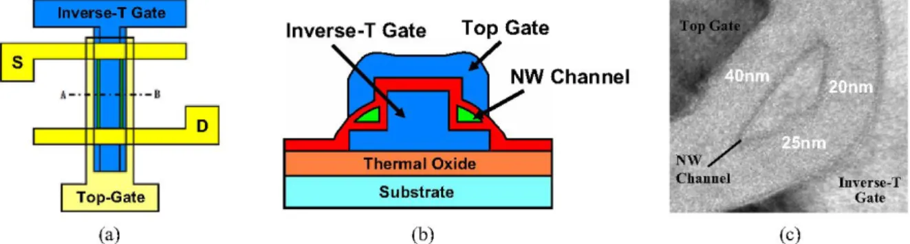
The two types of device structures are illustrated in Figs.1 and 2. The device fabrication shown in Fig.1 is similarto that described in our previous work, exceptthat the formation ofa top gate is added. The second type of
structure shown in Fig.2 applied twice the
lithography/etching process to form an inverse-T gate,
followed by the formation of NW channels. Note that the
height of upper step of the inverse-T gate was designedto
be higher than the lower one, so in the process we could
control theetching timeto allowonlytwoNWchannelsto
remainon the upper-stepcornersof the inverse-T gate. The
remaining process sequence is the same as that for the
formerstructure. TEMpictures of the devicesare shown in
Fig. l(c) and Fig. 2(c). Thickness of gate oxide is about
20nm. Dimensions of the NW structures aredifferent in the
twocases, owingtothe difference in stepheightandprofile
of the sidewall.
RESULTS AND DISCUSSIONS
Transfer characteristics of the two types of devices
under single-gate (SG) or double-gate (DG) modes of
operation are shown in Figs. 3(a) and (b). It can be seen
clearlythat the characteristics aredramatically improvedas
thetwo gates are tied together, thanksto the enhancement of gatecontrollabilityoverthe NW channels. Under the DG mode, subthreshold swings of 130 and 90 mV/dec. are achieved for thetwotypesof devices. The lattercaseshows better characteristics. This is ascribedto its thinnerbody as
well as the use of inverse-T gate. From the TEM image
shown in Fig. 2(c), the NW channel is almost fully surroundedbythe inverse-T gate and the top-gate, ensuring
agoodgatecoupling duringthe DG mode ofoperation.
Separate gates inanMGconfigurationcanincrease the flexibilityindevice operation. Figure4 shows theabilityof the device inmodulating the thresholdvoltage by the bias ranging form -3 to 3 V applying to the top gate. In the
figures, the transfer characteristics are clearly shifted by
varying the gate voltage. Threshold voltage and
subthresholdswingas afunction of top gate bias are shown in Fig. 5. The phenomena and trends we observed are
basically consistent with those presentedin previous work
[6].However, the device with inverse-T gate clearlyshows stronger gate-to-gatecouplingeffect.
CONCLUSIONS
In this work, two types of poly-Si nanowire (NW)
transistors with multiple-gate (MG) configuration were
fabricated and characterized. The devicesareequippedwith
two independent gates to increase the gate controllability
and device operation flexibility. With such MG
configurations, excellent device performance is
demonstrated, despitetheuseofpoly-SiNW. Foroneof the
MGconfiguration featuring aninverse-T gate, subthreshold
swing aslowas90 mV/dec is achieved. The adjustmentof
thresholdvoltagewith top-gate bias control is also explored
inthis work.
Acknowledgment-This work was supportedin partby
the National Science Council under contract No. NSC
95-2120-E-009-003.
REFERENCES
[1]F. L.Yangetal., in Symp. VLSI Tech. Dig., pp.196-197,2004.
[2]X. Duanetal.,NanoLett.,vol.2,pp.487-490,2002.
[3]Y.Cuietal., Science, vol. 293, pp.1289-1292,2001.
[4]H.C.Linetal.,IEEEElectronDeviceLett.,vol.26,pp.
643-645, Sep.2005.
[5]H.C.LinandC. J.Su,IEEETrans.Nanotechnology, vol. 6,pp.
206-212,Mar.2007.
[6]M. Masaharaetal.,IEEETrans.Electron Devices.,vol.52,pp.
2046-2053, Sep.2005.
Side Gate
TopGate
NW
Channel
(a) (b)
(c)
Fig. 1 (a) Topview, (b) cross-sectional structureand(c) cross-sectionalTEMview of the NWTFT with
side-gate
and top-gate structure....Inverse-T Gate
Top
Gate
NW
Channel
|
Top-Gate | SubstrateI I |
|
Gate| ||b|
(a)
(b)
(c)
Fig. 2 (a) Top view, (b) cross-sectional structure and(c) cross-sectionalTEMview of the NWTFT with
inverse-T-gate
and top-gatestructure. 10-6 10o7-SS 130 mV/dec 10U- L=0.8um,t,,=18.5nm *S10-1°0 \ VD=0-5,2 V 0-11 SweepVSG,VTG=OV SweepVTG VSG=OV 10-12 Sweepboth,VSG=VTG 10-13 -2 -1 0 1 2 3 4 5 GateVoltage(V) (a) 10-5 10-6 10-7 SS - 9OmV/dec 10-8 1 L 0.8um,t,=18.5nm 10-10 r VD=0.5,2V 10-11 SweePVITG, VTG=OV1o-12 \ } SweepVTG, VITG=OV
\ 1Sweenboth V.-r= V-r--2 -1 0 1 2 3 4 5 GateVoltage (V) (b) 0 0I 0 1 2 3 4 5 Side-GateVoltage(V) 0I -1 -2 -3 -4 -3 -2 -1 0 1 Top-GateVoltage(V) (a) 10-6 10-7 Z 10-8 0 10-10-10 10-11 -3 -2 -1 0 1 2 3
Inverse-T GateVoltage (V)
(b) 2 3 (a) 4 _10 3 ~~~~~~~~~~200 2 -190 -180 -170 -1 -2 -160 -3r. .i ... 150 -4 -3 -2 -1 0 1 2 3 4 Top-Gate Voltage (V) (b)
Fig. 3 Transfer characteristics of (a) type-I (Fig.1) and (b) type-II (Fig.2)
devices.
Fig. 4 Transfer characteristics of(a) type-I and (b) type-II devices with various top-gate biases.
Fig. 5 Extracted VTH and S.S. as a
function of top-gate biases for the results shown inFig.4.
E ui na n) eU-I Wl|||wlw|||l| -4i lUV- I.
.-I...
I~oweepDoirl,viTG.vTG
....I.... I.... I...I