A physical model for the hysteresis phenomenon of the ultrathin ZrO 2 film
J. C. Wang, S. H. Chiao, C. L. Lee, T. F. Lei, Y. M. Lin, M. F. Wang, S. C. Chen, C. H. Yu, and M. S. Liang
Citation: Journal of Applied Physics 92, 3936 (2002); doi: 10.1063/1.1498964
View online: http://dx.doi.org/10.1063/1.1498964
View Table of Contents: http://scitation.aip.org/content/aip/journal/jap/92/7?ver=pdfcov
Published by the AIP Publishing
Articles you may be interested in
Thickness dependence of structural and electrical characteristics of ZrO 2 thin films as grown on Si by chemical-vapor deposition
J. Vac. Sci. Technol. B 22, 1940 (2004); 10.1116/1.1776560
Structural and dielectric properties of thin ZrO 2 films on silicon grown by atomic layer deposition from cyclopentadienyl precursor
J. Appl. Phys. 95, 84 (2004); 10.1063/1.1630696
Effects of growth temperature on the properties of atomic layer deposition grown ZrO 2 films
J. Vac. Sci. Technol. A 21, 1359 (2003); 10.1116/1.1564032
Electrical characteristics of ultrathin ZrO 2 prepared by wet oxidation of an ultrathin Zr-metal layer
J. Vac. Sci. Technol. B 20, 400 (2002); 10.1116/1.1447245
Study of ZrO 2 thin films for gate oxide applications
J. Vac. Sci. Technol. A 19, 1720 (2001); 10.1116/1.1351802
A physical model for the hysteresis phenomenon of the ultrathin
ZrO
2film
J. C. Wang, S. H. Chiao, C. L. Lee,a) and T. F. Lei
Department of Electronics Engineering, National Chiao-Tung University, Hsinchu 300, Taiwan, Republic of China
Y. M. Lin, M. F. Wang, S. C. Chen, C. H. Yu, and M. S. Liang
Taiwan Semiconductor Manufacturing Company, Hsinchu 300, Taiwan, Republic of China 共Received 4 March 2002; accepted for publication 12 June 2002兲
This work studies and presents an inner-interface trapping physical model for the ultra-thin
共effective oxide thickness⫽15 Å兲 zirconium oxide 共ZrO2兲 film to explain its hysteresis phenomenon. The shift of the capacitance–voltage characteristics swept from accumulation to inversion and then swept back with light illumination is about 110 mV, which is larger than the shift without light illumination 共⬃45 mV兲. The mobile ion effect is obviated using bias-temperature stress measurement. The proposed model successfully explains not only the phenomenon but also the thickness effect for the capacitance–voltage characteristics and the different turn-around voltages of the current density–voltage characteristics of the zirconium dielectrics. © 2002 American Institute
of Physics. 关DOI: 10.1063/1.1498964兴
I. INTRODUCTION
For the very deep submicron complementary metal– oxide–semiconductor 共CMOS兲 device, the international technology roadmap for semiconductors共ITRS兲 predicts that a sub-16 Å silicon dioxide gate dielectric is needed for the sub-0.1m CMOS device.1A SiO2 gate oxide of that thick-ness has been shown to have a leakage current of the range of 1–10 A/cm2.2,3 Recently, there was much work4 –16 on studying ZrO2to replace SiO2as the gate dielectric due to its high dielectric constant 共⬃25兲, wide energy bandgap 共⬃7.8 eV兲,8high stability with the Si surface,17and low post depo-sition annealing temperature 共⬃500 °C兲.4Its electrical prop-erties were also reported to be good enough as the candidate for the gate dielectrics for the deep sub-micron device.
Unfortunately, for ZrO2, there is the hysteresis phenomenon in its capacitance–voltage 共C–V兲 characteristics.11,13,14,18 This hysteresis will induce a flat-band voltage shift, consequently a threshold voltage instabil-ity when it is applied to the MSO field-effect transistor as the gate dielectrics. It was reported that the hysteresis phenom-enon might be due to chemical contaminations, the stress-induced defect formation, or mobile ions.19 In this article, this phenomenon is studied and an inner-interface trapping model is presented to explain it.
II. EXPERIMENT
Al/TiN/ZrO2/Zr-silicate/p-Si capacitors with an area of 7.85⫻10⫺5 cm2 were fabricated on 8-in. p-type Si wafers. First, the ZrO2 film of 50 Å was deposited by atomic layer chemical vapor deposition, which was performed at a tem-perature of 300 °C and a pressure of about 1 Torr. The pre-cursors used for the deposition were ZrCl4 and H2O. After
the gate dielectric was formed, a TiN film of 250 Å was deposited by metal organic chemical vapor deposition. The sample was then annealed in the furnace for 10 min in an N2 ambient at 400 °C. A 5000 Å Al film was deposited on the wafer by a thermal coater. After that, the gate of the capacitor was defined lithographically and etched. Finally, a 5000 Å Al film was also deposited on the back side of the wafer to form the ohmic contact. The effective oxide thickness共EOT兲 was estimated by the high frequency 共0.1 MHz兲 C–V in the strong accumulation region without considering quantum mechanical effects. Moreover, the physical thickness was checked by a transmission electron microscopy 共TEM兲 to obtain the dielectric constant. The electrical properties were
a兲Electronic mail: [email protected]
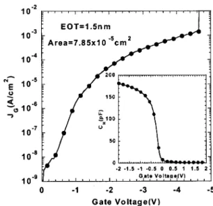
FIG. 1. Plots of negative current density vs voltage characteristics of the zirconium dielectrics, where the inset shows the high frequency capacitance vs voltage characteristics with the voltage swept from inversion to accumu-lation.
3936
0021-8979/2002/92(7)/3936/5/$19.00 © 2002 American Institute of Physics
measured by using an HP 4156B semiconductor parameter analyzer and an HP4284A precision LCR meter.
III. RESULTS AND DISCUSSION
Figure 1 shows the negative current density–voltage
共J–V兲 characteristics, where the inset shows the high
fre-quency C–V characteristics swept from inversion to accumu-lation, of the fabricated ZrO2film, for which the EOT value derived is 15 Å. The TEM micrograph of the cross section of the film is shown in Fig. 2, where the physical thickness was measured to be 53.7 Å. In the TEM picture, it is also ob-served that there exists an interfacial layer of about 10 Å, referred as Zr-silicate,20 at the ZrO2/Si interface. It is be-lieved that this silicate layer plays an important role in cre-ating the hysteresis observed in the zirconium dielectrics as explained later. The effective dielectric constant derived based on the physical thickness, including the interfacial Zr-silicate layer, is larger than 20. The sample shows a leakage current density lower than 10⫺6A/cm2 at Vg⫽⫺1 V, which is comparable with the values reported before.4 –7 Figure 3 shows the measured time-to-breakdown 共TBD兲 data of the dielectrics at room temperature and 150 °C respectively, and
FIG. 2. TEM image of the zirconium dielectrics.
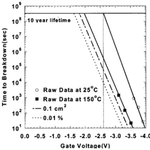
FIG. 3. The measured TBDdata of the sample at room temperature and the
150 °C respectively, and the derived TBDdata for the scaled area of 0.1 cm2
and the 0.01% failure rate for the samples.
FIG. 4. 共a兲 Hysteresis phenomenon of the zirconium dielectrics sweeping from accumulation 共solid line兲 and from inversion 共dashed line兲 without light illumination.共b兲 Hysteresis phenomenon of the zirconium dielectrics sweeping from accumulation with 共dashed line兲 and without 共solid line兲 light illumination. The hysteresis phenomenon sweeping from inversion is in inset.
FIG. 5. High frequency capacitance vs voltage distortion under bias-temperature stress of the zirconium dielectrics, where the inset shows the enlargement between 50 to 100 pF.
3937
J. Appl. Phys., Vol. 92, No. 7, 1 October 2002 Wanget al.
the derived TBDdata for the scaled area of 0.1 cm2 and the 0.01% failure rate for the samples.21,22In the above, the data for the area scaling and the 0.01% line were derived from the Weibull distribution of the 150 °C data assuming a random distribution of breakdown sites.23The derived maximum op-erating voltage could be, in these conditions, as high as 1.6 V, which is much higher than 1 V for the sub-0.1m device as obtained from the ITRS roadmap.
Figure 4共a兲 shows the hysteresis in the C–V characteris-tics of the sample without light illumination. The solid line is
FIG. 6. 共a兲 Inner-interface trapping model of the zirconium dielectrics sweeping from accumulation共Vg⫽⫺2.0 V兲 without light illumination. 共b兲
Inner-interface trapping model of the zirconium dielectrics sweeping from inversion共Vg⫽⫹1.0 V兲 without light illumination. 共c兲 Inner-interface
trap-ping model of the zirconium dielectrics sweetrap-ping from inversion 共Vg ⫽⫹1.0 V兲 with light illumination.
FIG. 7. Hsyteresis phenomenon of the zirconium dielectrics sweeping from accumulation for the thinner zirconium oxide共solid line兲 and thicker one 共dashed line兲 without light illumination.
FIG. 8. 共a兲 Absolute values of the current-density vs voltage characteristics sweeping from accumulation to inversion.共Turn-around voltage⫽⫺0.4 V兲. 共b兲 Absolute values of the current-density vs voltage characteristics sweep-ing from inversion to accumulation.共Turn-around voltage⫽⫹0.5 V兲.
the C–V characteristics for measuring the curve by sweeping the voltage from accumulation to inversion and then sweep-ing back 共⫺2.0 V⇒⫹1.0 V⇒⫺2.0 V兲. A shift of about 45 mV is observed. The dashed line is the curve measured by sweeping from inversion to accumulation and then sweeping back. A shift of 45 mV is also observed. However, when light was applied during the measurement, the shift increased to 110 mV, as shown in Fig. 4共b兲. To explore the reason for this phenomenon, a bias temperature stress 共BTS兲 of Vg
⫽⫾0.7 V, 125 °C for 30 min was applied to the sample. For
BTS of both positive and negative polarities, as shown in Fig. 5, no significant C–V curve shifts were observed. It was concluded that the hysteresis phenomenon was not caused by the mobile ion effect.
As revealed by the TEM picture of Fig. 2, there exists a thin silicate layer between the ZrO2and silicon substrate. An energy band diagram of the TiN/ZrO2/Zr-silicate/p-Si struc-ture was recently reported.24 Due to the imperfect structure of the interface between the ZrO2and Zr-silicate, it would be expected that this interface would act as charge trapping cen-ters. Therefore, an inner-interface trapping model as shown in Fig. 6 is proposed to explain the hysteresis phenomenon. When the capacitor is first at accumulation 共Vg⫽⫺2.0 V兲, majority carriers 共holes for the p-type Si substrate兲 tunnel from p-Si substrate through the Zr-silicate layer and are trapped at the inner-interface, as shown in Fig. 6共a兲. When the voltage is swept toward the positive direction, the C–V curve shifts negatively. Then, when the voltage is swept to the positive side to make the capacitor stay at inversion
共Vg⫽⫹1.0 V兲, the trapped holes at the inner-interface will be de-trapped and at the same time minority carriers 共elec-trons兲 will tunnel from the p-Si substrate and trapped at the inner-interface, as shown in Fig. 6共b兲. This makes the C–V curve shift positively when the voltage is swept toward the negative side. The mechanism makes the C–V curve have a hysteresis loop. As a light illumination is applied to the semi-conductor, electron–hole pairs will be generated 关see Fig. 6共c兲兴, which make the above phenomenon more evident. Es-pecially, the light illumination makes a more significant ef-fect on minority carriers as seen from Fig. 4共b兲, where a larger voltage shift of 110 mV was observed for the voltage sweeping from inversion toward accumulation. The change on the majority carrier concentration was insignificant, thus making almost the same C–V curve as the voltage was swept from accumulation toward inversion.
Figure 7 shows the C–V curve shifts for two different thicknesses of the zirconium dielectrics. It shows that the thicker zirconium dielectric 共dashed line兲 has a larger C–V curve voltage shift共100 mV兲 than that 共45 mV兲 of the thin-ner. Based on our proposed model, as the thickness of the zirconium dielectrics increases, the relative distance of the inner-interface as compared to the total thickness of the di-electrics will be closer to the silicon substrate, resulting more shift of the C–V curve. Figures 8共a兲 and 8共b兲 show the ab-solute current density–voltage 共兩J兩–V兲 characteristics of the dielectrics measured with the voltage swept from accumula-tion to inversion and from inversion to accumulaaccumula-tion respec-tively. For Fig. 8共a兲, the current is negative and becomes positive at the gate voltage equaling ⫺0.4 V, but for Fig.
8共b兲, the current is positive and becomes negative at the gate voltage equaling ⫹0.5 V. This difference in the turn-around voltages of the current can also be explained by using the inner-interface trapping model. As the capacitor is at the ac-cumulation region, holes are trapped at the inner-interface
关see Fig. 6共a兲兴, making the turn-around voltage of the current
be at ⫺0.4 V when the gate voltage is swept toward the inversion region; while as the capacitor is at the inversion region, electrons are trapped at the inner-interface 关see Fig. 6共b兲兴, making the turn-around voltage of the current be at
⫹0.5 V when the gate voltage is swept towards
accumula-tion.
IV. CONCLUSION
In conclusion, the hysteresis phenomenon of the zirco-nium dielectrics can be explained by using an inner-interface trapping model. The influence of light illumination on the hysteresis phenomenon is quite serious because of more charges trapped at the ZrO2/Si-silicate interface. The model well explains not only the hysteresis effect but also the thick-ness effect of the C–V characteristics and the different turn-around voltages on the J–V characteristics of the zirconium dielectrics capacitor.
ACKNOWLEDGMENTS
The authors would like to thank ASM Far East Market-ing Ltd. and National Nano Device Laboratory, ROC, for their technical help, and National Science Council, ROC, for their financial support under Contract No. NSC90-2215-E009-070.
1TSIA NEWS, ITRS 2000 Update Conference, December 2000. 2H. Sasaki, M. Ono, T. Yoshitomi, T. Ohguro, S. Nakamura, M. Saito, and
H. Iwai, IEEE Trans. Electron Devices 42, 1233共1996兲.
3
G. Timp et al., Tech. Dig. - Int. Electron Devices Meet. 1998, 615.
4
Y. Ma, Y. Ono, L. Stecker, D. R. Evans, and S. T. Hsu, Tech. Dig. - Int. Electron Devices Meet. 1999, 136.
5W.-J. Qi, R. Nieh, B. H. Lee, L. Kang, Y. Jeon, K. Onishi, T. Ngai, S.
Banerjee, and J. C. Lee, Tech. Dig. - Int. Electron Devices Meet. 1999, 132.
6W.-J. Qi, R. Nieh, B. H. Lee, K. Onishi, L. Kang, Y. Jeon, J. C. Lee, V.
Kaushik, B.-Y. Nauyen, L. Prabhu, K. Eisenbeiser, and J. Finder, Tech. Dig. VLSI Symp. 2000, 33.
7C. H. Lee, H. F. Luan, W. P. Bai, S. J. Lee, T. S. Jeon, Y. Senzaki, D.
Roberts, and D. L. Kwong, Tech. Dig. - Int. Electron Devices Meet. 2000, 27.
8C. H. Lee, Y. H. Kim, H. F. Luan, S. J. Lee, T. S. Jeon, W. P. Bai, and D.
L. Kwong, Tech. Dig. VLSI Symp. 2001, 137.
9
Z. J. Luo, T. P. Ma, E. Cartier, M. Copel, T. Tamagawa, and B. Halpern, Tech. Dig. VLSI Symp. 2001, 135.
10M. Balog, M. Schieber, M. Michman, and S. Patai, Thin Solid Films 47,
109共1977兲.
11G. D. Wilk and R. M. Wallace, Appl. Phys. Lett. 76, 112共2000兲. 12
M. Copel, M. Gribelyuk, and E. Gusev, Appl. Phys. Lett. 76, 436共2000兲.
13T. Ngai, W. J. Qi, R. Sharma, J. Fretwell, X. Chen, J. C. Lee, and S.
Banerjee, Appl. Phys. Lett. 76, 502共2000兲.
14C. M. Perkins, B. B. Triplett, P. C. McIntyre, K. C. Saraswat, S. Haukka,
and M. Tuomminen, Appl. Phys. Lett. 78, 2357共2001兲.
15
T. S. Jeon, J. M. White, and D. L. Kwong, Appl. Phys. Lett. 78, 368
共2001兲.
16G. D. Wilk, R. M. Wallace, and J. M. Anthony, J. Appl. Phys. 87, 484 共2000兲.
17
R. B. Beyers, Ph.D thesis, Stanford University共1989兲.
18G. D. Wilk and R. M. Wallace, Appl. Phys. Lett. 74, 2854共1999兲. 19L. Kim, J. Kim, D. Jung, and Y. Roh, Appl. Phys. Lett. 76, 1881共2000兲.
3939
J. Appl. Phys., Vol. 92, No. 7, 1 October 2002 Wanget al.
20T. Yamaguchi, H. Satake, and A. Toriumi, 2000 International Conference
on Solid State Devices and Materials, 2000, p. 228.
21J. H. Stathis and D. J. DiMaria, Tech. Dig. - Int. Electron Devices Meet. 1998, 167.
22R. Degraeve, N. Pangon, B. Kaczer, T. Nigam, G. Groeseneken, and A.
Naem, Tech. Dig. VLSI Symp. 1999, 59.
23
R. Degraeve, G. Groeseneken, R. Bellens, J. L. Ogier, M. Depas, P. J. Roussel, and H. E. Maes, IEEE Trans. Electron Devices 45, 904共1998兲.
24T. Yamaguchi, H. Satake, N. Fukushima, and A. Toriumi, Tech. Dig. - Int.
Electron Devices Meet. 2000, 19.