Pergamon
Solid-State &lrrtronic~ Vol. 39. No. 5. pp. 689493. 1996 003%1101(95)00155-7 Printed in Great Britain. Copyright kr 1996 Elsevier Science Ltd All rights reserved 0038-I lOI/ 515.00 + 0.00
A NOVEL
TWO-STEP
ETCHING
PROCESS
FOR
REDUCING
PLASMA-INDUCED
OXIDE
DAMAGE
KUO-FENG YOU and CHING-YUAN WU
Advanced Semiconductor Device Research Laboratory and Institute of Electronics. National Chiao-Tung University, Hsinchu, Taiwan. Republic of China
(Received 25 April 1995, in reoised,form 16 June 1995)
Abstract-During plasma etching, a large amount of charging current due to plasma can flow through the gate oxide near the endpoint, resulting in the degradation of thin gate oxide. In this paper. a two-step etching process using reactive ion etching (RIE) following wet etching is proposed to reduce the gate oxide charging current. The characteristics of the proposed process for gate oxide protection are characterized by time-dependent dielectric breakdown (TDDB), high-frequency capacitance-voltage (HFCV), and quasi- static capacitanceevoltage (QSCV) measurements. From measurement results, it is shown that degradation of the gate oxide is dramatically eliminated by the proposed two-step etching method as compared with that using pure RIE. Therefore, the proposed two-step etching process can replace the pure dry etching process to reduce the plasma-induced gate oxide damage.
1. INTRODUCTION
Plasma processes are extensively used in modern VLSI fabrication. As a wafer is exposed in the non- uniform plasma environment, charge build-up can occur on its surface. and the MOS devices fabricated on the wafer can be degraded due to electrical stressing. This problem becomes much more serious in multi-layer metal technologies because the charges introduced by plasma processes can be built up through not only floating polysilicon but also poly- silicon electrically connected to the interconnection metal or polysilicon lines. The metal or polysilicon line (called “antenna”) may amplify the charging effects by a factor of the interconnection layer to the thin gate oxide area ratio (called “antenna ratio”), inducing trap charges in the gate oxide as well as interface states at the SiOZ-Si interface. Gate oxide damage due to wafer charging has been reported for different plasma processes such as polysilicon gate etching[ 11, aluminum etching[2], and photoresist ashing[3], etc. Several researchers have related the damages with the edge of the gate or interconnect layer during plasma processes[4,5]. During plasma ashing processes, plasma charges are collected by the top surface of the gate or interconnect layer. How- ever, the charges can be collected by the sidewall of the gate/interconnect layer or by surfaces which are not covered by the photoresist during the plasma etching process or plasma overetching. During the dry etching process, there is a great amount of charg- ing current flowing through the gate oxide at the endpoint due to plasma non-uniformity[6], and the resulting oxide charging current will degrade the thin gate oxide.
Several researchers have studied plasma-induced oxide damage. Fang et a/.[71 have proposed an equiv- alent circuit model for the wafer charging in fion- uniform plasma during the ashing process to calculate the gate oxide charging current and associated, the oxide failure with the charging current. Shin et al@] have developed a quantitative model for thin oxide plasma charging damage by examining the oxide thickness dependence of the charging current. Gabriel and Weling[9] have proposed a method of usiog a protective dielectric layer (a thermally deposited TBOS oxide) on top of the gate electrode to minimize charge penetration during wafer fabrication. Although several models were proposed to model the damage effect[7,8] or to reduce the damage during the ashing process[9], little work has concentrated on the etching process architectures which are inherently less sensitive to damage.
In this paper, a new etching process is proposed to eliminate the gate oxide charging current dut to plasma, which uses a two-step etch polysilicon process. RIE is used to etch most of the polysilicon. followed by wet etching used near the endpoint to reduce the gate charging oxide current. The integrity of the gate oxide fabricated by three different etching conditiDns, i.e. pure RIE, two-step etching, and pure wet etching, has been characterized. It is shown that the proposed two-step process may preserve the quality of thin kate oxides as compared to that using pure RIE.
2. EXPERIMENTAL PROCEDURES
To study the plasma-induced oxide damage dufing the plasma etching process, the polysilicon gate MOS capacitors were fabricated on 4-inch (100) n-type 689
Table 1. The process conditions for the test samples
Samples Process conditions Sample 1 RIE I2 min + wet etching 20 s Sample II RIE ISmin
Sample 111 Wet etching 105 s
Note: the volume ratio of the wet etching solution is 64% HNO,. 33% H,O, and 3% NH,F.
substrate Si wafers. The thin gate oxide of 14 nm was grown in dry O2 at 85O”C, and then the phosphorus- doped polysilicon gate of 400 nm was deposited on the gate oxide film. After gate definition, the poly- silicon gate etching carried out under three etching conditions, as shown in Table 1. The three etching conditions are 15 min for pure dry etching with chemical species and process conditions: CF, 40 seem, O2 5 seem pressure, 100mtorr pressure, 50 Watt RF power, 105 s for pure wet etching, and 12 min for dry etching following by 20 s of wet etching (two-step etch). Samples I-III were fabricated by two-step etching, pure dry etching and pure wet etching, respectively. The volume ratio of the wet etching solution is 64% HNO,, 33% H,O, and 3% NH,F, and the etching rate of wet etching solution is 2000 A/min. If the wet etching time is 20 s, we have about 0.06pm undercut, therefore the undercut problem is not serious when using the two-step etching process. The gate oxide areas of samples I-III are 1.114 x 10m3cm2, 1.116 x 10⁻³cm2 and 1.050 x 10m3 cm2 using SEM measurement, respectively, which are very large compared to the slight undercut during wet etching. Therefore, the area of the capacitor fabricated by pure wet etching can be neglected for the present studies due to the slight undercut of the polysilicon using wet etching.
To characterize oxide damage after exposure in the plasma environment, the fast ramp-voltage breakdown test was used. The charge-to-breakdown,
Q M,
was measured by the time-dependent dielectric breakdown (TDDB) technique using a constant- current stress of 100mA/cm2 for charge injection from substrate, and the interface-state densities were determined from high-frequency capacitance-voltage (HFCV) and quasi-static capacitano+voltage (QSCV) measurements by using a constant current stress of100 PA/cm’.
3. RESULTS AND DISCUSSION
Under a non-uniform plasma environment, the voltage is built up on the gate oxide by collected plasma charges. The built-up voltage must force an oxide current to relieve the voltage before the gate oxide breakdown is reached. Therefore, there is a large amount of gate oxide charging current flowing through the thin gate oxide during pure dry etching near the endpoint, as shown in Fig. 1. The large charging current will generate the latent gate oxide trapped charges and interface states. The generated trap-charges may induce a reliability failure and the
Early stage Near cnd~mint During overetch
+- +- C-
Poly
Q
_-Fig. I. The schematic diagrams showing oxide damage during poly-Si etching. Initially, the surface current prevents charging. Near the endpoint, the long surface conduction paths across the wafer become too resistive, and the excess current charges the gate and flows through the substrate. During overetching, the collected current is limited by the
small sidewall area[6].
generated interface states may degrade MOS transistor characteristics such as subthreshold slope, trans- conductance, and device lifetime. Although there is no gate oxide charging current during pure wet etching, non-uniform etching rate and serious under- cut render wet etching infeasible in modern VLSI
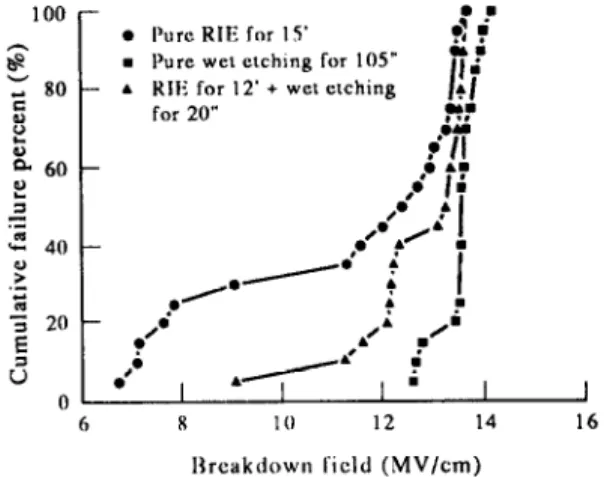
. I’urc RIE for 15’ 2: r . Pure wet etchmg for 105” - & RIE for 12’ + wet etching I
‘ii *I for 20” RF 97 \I 6 8 I 0 12 14 16 IIrcakdown field (MV/cm)
Fig. 2. The measured breakdown field of oxides from three test samples.
. Pure RIE ror 15’
n Pure wet etching for 105” ’ f :* A Klli for 12’ + wet etching l I
ror 20” 1 $
p;*- ,* ,j y; , ,
10 20 30 40
Charge-to-breakdown (C/cm2) Fig. 3. The measured charge-to-breakdown of oxides from
A novel two-step etching process for reducing plasma-induced oxide damage 691 fabrication. The two-step etching process cannot only
reduce the gate oxide charging current by using wet etching near the endpoint, but also eliminate the charges built on the gate electrode during plasma overetching. Besides, the critical dimension loss could be reduced if we reduce the wet etching time and/or the etching rate of the wet solution. In general, the reduction of the etching rate using dilute solution becomes the best choice. Therefore. under the same etching time, the undercut due to wet etching should be much reduced and this renders the two-step etch- ing process more feasible in deep submicron tech- nology. At the same time, the proposed process can reduce the plasma-induced oxide damage dramatically.
the two-step etching process does have a dramatic improvement on breakdown field and charge-to- breakdown as compared with that using pure reactive ion etching. In this paper, the fabricated MOS cqpaci- tors are characterized to see the effects of difterent etching processes. If the antenna structure is used, the incorporated field oxide capacitors will enlarge the gate oxide charging current near the dry-etch endpoint due to charge redistribution and the differ- ence in performance between pure dry etching step and two-step etching process will become larger. Therefore, the improvement due to two-step etching should be significant.
The cumulative failure percent of breakdown field
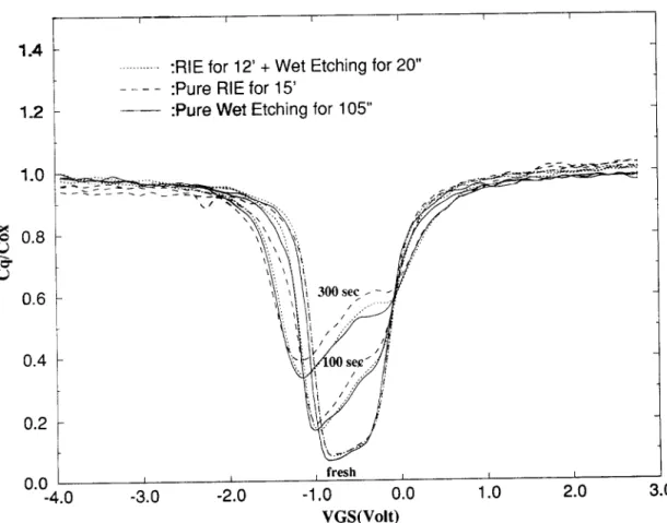
The quasi-static capacitance-voltage (QSCV) ourves measured from three different test MOS capacitor and charge-to-breakdown for three different etching samples are shown in Fig. 4. The stress timers are processes, i.e. pure reactive ion etching (RIE). pure 0, 100, 300 s, respectively, for a constant current wet etching, and two-step etching, are shown in Figs 2 stress density of 100 pAA/cm’. From Fig. 4, it is clearly and 3. The measured breakdown fields are 13.2 MV/ shown that the quasi-static capacitance-voltage cm and 13.5 MV/cm for two-step etching and pure wet curves of the pure wet etching step and the two-step etching, respectively. It is clearly seen that significant etching are almost the same. Consequently, the oxide damage occurs when pure reactive ion etching performance of the MOS capacitor fabricated by is used. From Fig. 3, the curves of charge-to-break- the two-step etching process is as good as the device down for two-step etching and fully wet etching are fabricated by pure wet etching. The QSCV curve of almost coincident and Qhd is near 28 C/cm’ for two- pure RIE moves upward compared with the curves step etching and pure wet etching, but Qbd is just of pure wet etching and two-step etching. It implies 21 C/cm’ for pure dry etching. It is clearly shown that that the pure RIE step generates more interfacebstate
:RIE for 12’ + Wet Etching for 20”
:Pure RIE for 15’
:Pure Wet Etching for 105”
“0 0.8
u
3
u
0.6
0.4
0.0
1
I I , fresh I I ,-4.0
-3.0
-2.0
-1.0
0.0
1.0
2.0
3.0
VGS(Volt)
Fig. 4. The measured quasi-static capacitance-voltage curves from three test samples. The stress times are 0. 100, 300 s, respectively.
9.0 -
-0.6
---
:RIE for 12’ + Wet Etching for 20”
:Pure RIE for 15’
-
:Pure Wet Etching for 105”
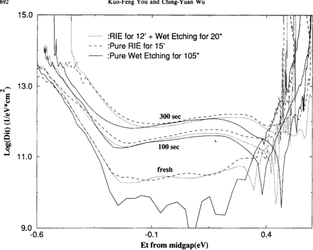
Et from midgap
Fig. 5. The measured distribution of generated interface-state density in the energy bandgap from three test samples. The stress times are 0, 100, 300 s, respectively.
densities. The distribution of generated interface-state densities in the energy gap is shown in Fig. 5. From Fig. 5, we obtain less latent interface-state density using the two-step etching process than that using pure RIE etch. The midgap interface-state densities for three different samples are shown in Fig. 6. It is clearly seen that the generated interface-state density using the two-step etching process exhibits the smallest magnitude after 300 s stress and becomes
-2 12
0 r
.Pure RIE for 15’
; IO-
. Pure wet etching for 105” .
u & RIE for 12’ + wet etching .
> for 20” . s 8 c a 1 6 “E 4 I 100 200 300 Stress time (s)
Fig. 6. The midgap interface-state density measured from three test samples.
saturated after a long time of stressing. This result completely shows the advantages of the two-step etching process.
4. CONCLUSION
We have demonstrated that the proposed two-step etching method can achieve a similar oxide quality to that obtained by pure wet etching without inducing the undercut problem if the proper etching rate for polysilicon is chosen. The TDDB measurements show that the novel two-step etching process can give a higher breakdown voltage and charge-to-breakdown for the gate oxide compared with that using the pure plasma etching. The QSCV and HFCV measure- ments also show that the two-step etching process can reduce the generated latent interface-state densities due to plasma etching. Therefore, the gate oxide damage during plasma etching can be dramatically eliminated by using the two-step etching process instead of the pure plasma etching in CMOS technology.
Acknowledgemenr-The authors would like to express their sincere thanks to the National Science Council, Taiwan, Republic of China, for continuous grant support under contract NSC-85-22 I5-EOO9-041. Special thanks are given to Submicron Technology Research Institute, Taiwan, Republic of China, for providing the test devices, especially to Mr M. C. Chang.
A novel two-step etching process for reducing plasma-induced oxide damage 693
REFERENCES 5. S. Fang and J. P. McVittie, Appl. Phys. L&r. 62, 1507 (1993).
I. I.-W. Wu, M. Koyanagi, S. Holland, T. Y. Huang, J. C. Mikkelsen, Jr, R. H. Bruce and A. Chiang, J. Electrochem. Sot. 136, 1638 (1989).
2. H. Shin, C.-C. King, T. Horiuchi and C. Hu, IEEE Elecfron Device Lert. 12, 404 (1991).
3. Y. Kawamoto. Proc. 7th Symp. Dry Proc., p. 74 (1989).
6. S. Fang, S. Murakawa and J. P. McVittie, IEEE Int. Elec. Dev. Meet. (IEDM), Technical Dig., p. 61 (1992).
7. S. Fang, S. Murakawa and J. P. McVittie, IEEE Trans. Electron Devices 41, 1848 (1994).
8. H. Shin, K. Noguchi and C. Hu, IEEE Electron Device Left. 14, 509 (1993).
4. H. Shin and C. Hu, IEEE Electron Device Left. 13, 600 9. C. T. Gabriel and M. G. Weling, IEEE Electron Device