Thermal stability of Si/Si
12x2yGe
xC
y/Si quantum wells grown by rapid
thermal chemical vapor deposition
C. W. Liua) and Y. D. TsengDepartment of Electrical Engineering, National Taiwan University, Taipei, Taiwan M. Y. Chern
Department of Physics, National Taiwan University, Taipei, Taiwan C. L. Chang and J. C. Sturm
Department of Electrical Engineering and Center for Photonics and Optoelectronic Materials, Princeton University, Princeton, New Jersey 08544
~Received 27 April 1998; accepted for publication 10 November 1998!
The thermal stability of Si/Si12x2yGexCy/Si quantum wells was studied by high resolution x-ray
diffraction, Fourier transform infrared spectroscopy, and defect etching. There are different pathways of strain relaxation in this material system, depending on the annealing temperature. The lattice structure of Si12x2yGexCywas as stable as the Si12xGexalloys at an annealing temperature
of 800 °C for 2 h. At an annealing temperature of 900 °C for 2 h, the structures of both Si12x2yGexCy and Si12xGex started to relax. The addition of C enhanced the Ge outdiffusion in
Si12x2yGexCy, compared to that of Si12xGex. For the annealing temperatures of 950 and 1000 °C
for 2 h, the Si12xGex continued to relax with the decrease of strain in the quantum wells, but the
Si12x2yGexCyrelaxed with the increase of the strain due to the formation of SiC precipitates. Misfit
dislocation formation was observed in the Si12x2yGexCy alloys with initial thicknesses below the
critical thickness after annealing at 1000 °C for 2 h. This relaxation is probably caused by the SiC precipitation, since SiC precipitates can reduce the strain compensation and, therefore, decrease the critical thickness. © 1999 American Institute of Physics.@S0021-8979~99!06704-3#
I. INTRODUCTION
Recently there has been impressive progress in the growth1,2 and characterization3–6 of Si12x2yGexCy alloys, which offer great flexibility in tailoring the strain and the electronic properties of group IV heterostructures.7,8Because the lattice constant of cubic carbon ~diamond! is 0.356 683 nm,9 which is 34% smaller than that of Si, substitutional incorporation of C can compensate in the compressive strain of Si12xGexlayers grown on Si substrates, where the lattice
constant of Ge is 4.17% larger than that of Si. This leads to an increase in the critical thickness of pseudomorphic Si12x2yGexCy layers on Si. Since the formation of SiC
pre-cipitates is thermodynamically favored, the thermal stability of the Si12x2yGexCy alloys will not only be affected by the
misfit dislocation formation and Ge~C!/Si interdiffusion, which are inherent in Si12xGex alloys,
10–13
but also by the SiC precipitation. It was also reported that the carbon incor-poration into Si12xGex layers has the effect of suppressing
the boron outdiffusion in Si/Si12x2yGexCy/Si heterojunction
bipolar transistors.8 Therefore, it is important to investigate the thermal stability of Si12x2yGexCy alloys for further
de-vice applications. Previous study14 on Si12xCx/Si
superlat-tices grown by molecular beam epitaxy ~MBE! showed that SiC precipitated at annealing temperatures of 1000 °C and above, and that the structure relaxed only by interdiffusion at 900 °C and below. The low temperature annealing~,800 °C!
of the single thick MBE-grown Si12xCxsample15showed no
significant change in the strain and thickness. In this article, we have investigated the stability of Si12x2yGexCy alloys
grown by rapid thermal chemical vapor deposition~RTCVD! at different annealing temperatures by using high resolution x-ray diffraction ~XRD!, Fourier transform infrared ~FTIR! spectroscopy, and defect etching.
II. GROWTH
The Si12x2yGexCysingle quantum wells were grown on
Si ^100& substrates by RTCVD. The Si12x2yGexCy layers
were grown at 625 °C using methylsilane as the C source. The growth pressure was 6 Torr. The gas flows were 3 slpm for a hydrogen carrier, 26 sccm for dichlorosilane, and 0.8 sccm for germane. The maximum content of carbon incorpo-ration is around 2%. The Si cap layer was grown at 700 °C using a 26 sccm dichlorosilane flow and a 3 slpm hydrogen flow. The Ge fraction and thickness of Si12xGexwere
deter-mined by fitting x-ray rocking curves. Details of the Si12x2yGexCy growth can be found in Ref. 2. As small amounts of methylsilane were added to the source gases, we observed a shift in the ~400! x-ray diffraction peak of the resulting Si12x2yGexCy layers away from that of a similar layer without the addition of methylsilane. Vegard’s law with a compensation ratio of 1% C to 8.3% Ge was used1,2to estimate the carbon concentration in the alloys. The carbon content was obtained from the shift of~400! peak by assum-ing the Ge concentration was unchanged as the methylsilane was added. The thickness of the as-grown Si12x2yGexCy
a!Electronic mail: [email protected]
2124
mass spectroscopy ~SIMS! also has confirmed the existence of flat C profiles, and that Ge concentration was unchanged by adding the methylsilane on calibrated samples.
Three quantum well structures were investigated in this study. The well compositions were Si0.77Ge0.23, Si0.762Ge0.23C0.008, and Si0.758Ge0.23C0.012with thicknesses of 20, 18, and 18 nm, respectively. The nominal thickness of the Si cap was about 60 nm. The Ge content and thickness were obtained from dynamic simulation of the rocking curves, assuming a box profile. All as-grown samples were pseudomorphic and fully strained due to the low temperature growth ~625 °C!. No defect was observed in these as-grown films after defect etching, using four parts of 49% HF and five parts of 0.3 M CrO3. For a reference, the critical thick-nesses of the Si0.77Ge0.23, Si0.762Ge0.23C0.008, and Si0.758Ge0.23C0.012samples were 10, 17, and 23 nm, respec-tively, estimated from Matthews and Blakeslee’s theory.12,16,17The thickness of the Si0.77Ge0.23control sample was above its critical thickness, indicating that further relax-ation could be caused by dislocrelax-ation formrelax-ation and/or atomic interdiffusion. The thickness of the highest carbon-content sample (Si0.758Ge0.23C0.012) is well below its critical thick-ness, indicating that the relaxation mechanism could be in-terdiffusion and/or SiC precipitation. However, misfit dislo-cation formation can be also observed in these thin Si12x2yGexCy films, if the SiC precipitates can reduce the
strain compensation and thus decrease the critical thickness. Please note that the interdiffusion and/or the misfit disloca-tion formadisloca-tion would decrease the vertical lattice constant, but the SiC precipitation can increase the vertical lattice con-stant because of the consumption of Si and C atoms during the formation of SiC precipitates. The increase of the vertical lattice constant by 1 at.% of SiC formation in Si12x2yGexCy
is effectively the same as that by 8.3 at. % of Ge incorpora-tion.
III. CHARACTERIZATION AND DISCUSSION
To study the thermal stability of the Si/Si12x2yGexCy/Si
quantum wells, the x-ray rocking curves from as-grown and annealed samples were measured. The samples were an-nealed at temperatures from 800 to 1000 °C in nitrogen. To avoid nonuniformity of the 100 mm wafer, an accumulative annealing scheme was adopted. In other words, the annealing treatment was performed on the same pieces of samples at different temperatures. For all three samples annealed at 800 °C for 2 h, there was no change in the rocking curves, indicating that these structures are stable during a low-temperature process. This is similar to previous results.14The C incorporation into Si12xGex does not degrade the thermal
stability of the lattice structure at 800 °C. However, for all samples continuously annealed at 900 °C for 2 h, we ob-served a shift toward the Si peak in the ~400! x-ray rocking curves shown in Figs. 1, 2 and 3 for the Si0.77Ge0.23, Si0.762Ge0.23C0.008, and Si0.758Ge0.23C0.012 quantum well samples, respectively, indicating that all the structures started
to relax. To further probe the relaxation, the x-ray rocking curves were fitted with simulation profiles. The diffused Ge profile was taken from the solution of the one dimensional interdiffusion equation,18
xGe~z!5xGe0 /2$2erf@~2W/21z!/2L#
1erf@~W/21z!/2L#%,
where xGe0 is the initial Ge concentration, W is the quantum well thickness, z is the position along the growth direction (z50 at the well center!, erf is the error function, and L is the diffusion length. As the result of the SIMS profile,19the width of carbon profile is relatively unchanged during the annealing. We, therefore, assume a box carbon profile and
FIG. 1. High resolution x-ray diffraction spectra of Si/Si0.77Ge0.23/Si
quan-tum wells annealed at different temperatures. The well thickness is 20 nm. The~400! diffraction peak of the Si0.77Ge0.23layer continued to shift towards
the~400! Si peak as the annealing temperature increased.
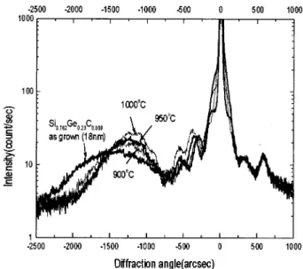
FIG. 2. High resolution x-ray ~400! diffraction spectra of Si/Si0.762Ge0.23C0.008/Si quantum wells annealed at different temperatures.
the width remaining constant, but the carbon concentration is left as a fitting parameter. The diffused Ge profile and the box carbon profile yield the narrowing of ~400! diffraction peak of Si12x2yGexCyin the diffraction spectra after
succes-sive annealings. The simulation also shows that the carbon box profile enhances the amplitude of the thickness fringe in the~400! diffraction spectra. Therefore, the fringes are more visible in the carbon-containing samples than in the Si12xGex samples. The relaxation parameter R, describing
the misfit dislocation formation, is defined by
R5~ap2aSi!/~ar2aSi!, ~1! where ap is the in-plane lattice constant of Si12x2yGexCy
alloys, ar is the lattice constant of fully relaxed
Si12x2yGexCylayers, and aSiis the lattice constant of the Si substrates. The shape of the ~400! diffraction is determined by the diffusion length L. The relative position of the~400! diffraction peak with respect to the Si ~400! peak is deter-mined by the carbon concentration, the relaxation parameter, and the diffusion length which changes the center concentra-tion in Ge profiles after the annealing. The diffusion length L can be extracted by fitting the simulation profiles with rock-ing curves. The carbon concentrations and relaxation param-eters cannot be extracted individually without further mea-surements. A typical simulation curve is shown in Fig. 4, where the relaxation parameter is assumed to be zero. Note that we can have different sets of carbon concentrations and relaxation parameters to fit the experimental curves. The ex-tracted diffusion length increases as the carbon content in-creases in the alloys ~Fig. 5! for all the annealing tempera-tures. This indicates that the incorporation of carbon can enhance the Ge diffusion in Si. Since transient enhanced dif-fusion was observed in CVD-grown SiGe quantum wells,11 the diffusion coefficients could not be extracted directly from the diffusion length. We have also observed some nonlinear diffusion in our samples, but details of it are still under investigation.
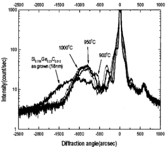
The same pieces of samples were annealed again at 950 °C for 2 h. The ~400! peak of the Si0.77Ge0.23 control sample continued to shift towards the Si ~400! peak. The peak of the Si0.762Ge0.23C0.008 sample shifted less than the control samples. The peak of high carbon-content sample (Si0.758Ge0.23C0.012) even had a slight tendency to shift to-wards the opposite direction, which indicated that the lattice constant of this sample started to increase. This is probably due to the formation of SiC precipitates, since only a de-crease of carbon content in the Si12x2yGexCy can increase
the vertical lattice constant. To confirm this observation, we annealed these samples at 1000 °C for another 2 h. Similar behavior was observed. The vertical lattice constant of the Si0.77Ge0.23control sample continued to decrease, and that of the Si0.762Ge0.23C0.008sample decreased very slightly, but that of the Si0.758Ge0.23C0.012sample continued to increase ~Fig. 6!.
FIG. 3. High resolution x-ray ~400! diffraction spectra of Si/Si0.758Ge0.23C0.012/Si quantum wells annealed at different temperatures.
The well thickness is 18 nm.
FIG. 4. Typical simulation curve to fit the~400! diffraction spectrum. The insert shows the Ge and C profiles used in the simulation.
To study the change of the material structures after 1000 °C annealing, FTIR absorption measurements were per-formed. The FTIR spectrum ~Fig. 7! of an as-grown 40 nm Si0.698Ge0.28C0.022layer shows a sharp absorption peak at 600 cm21, which is characteristic of the vibration frequency of substitutional carbon in silicon.2Note that in the FTIR mea-surement a thick layer is used to increase the absorption sig-nal. However, in the spectrum of the same sample after an-nealing at 1000 °C, the 600 cm21absorption peak vanished within the detection limit, and a broad peak from 670 to 900 cm21was observed, very similar to the absorption spectrum of amorphous silicon carbide.2,20 This indicated that some carbon atoms came out of the substitutional lattice and formed silicon carbide precipitates.
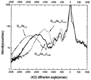
To further resolve the relaxation due to misfit dislocation formation and the residual carbon content in the Si12x2yGexCy alloys, we measured the asymmetrical~422!
diffraction of all three 1000 °C-annealed samples ~Fig. 8!. Following the approach in Ref. 21, the in-plane lattice con-stant can be obtained, which is a function of the relaxation parameter and the residual carbon content @Eq. ~1!#. Note that the Ge content at the center of the quantum well is determined by the diffusion length, and is not a free param-eter. To fit the relative position of the~400! diffraction of the Si12x2yGexCy alloys with respect to the~400! Si substrate,
we can have different sets of relaxation parameters and car-bon contents. A unique solution to the relaxation parameter and residual carbon content can be determined to satisfy both the in-plane lattice constants and the~400! diffraction spectra of the Si12x2yGexCy alloys. The results of the relaxation parameters and the residual carbon contents are given in Table I. The difference between the initial carbon concentra-tion and the residual carbon content is the amount of SiC precipitates. The atomic fractions of SiC precipitates are 0.0072 and 0.0084 for Si0.762Ge0.23C0.008 and Si0.758Ge0.23C0.012, respectively. The degree of relaxation in-creased with the amount of SiC precipitates. The SiC pre-cipitates may be responsible for the misfit dislocation forma-tion in the thin layers, because the precipitates reduce the strain compensation and decrease the critical thickness to approximately 15 nm for these two Si12x2yGexCy samples.
Therefore, after annealing, the thickness of these two Si12x2yGexCy samples ~18 nm! was beyond the critical
thickness and misfit dislocation formation occurred. These
FIG. 6. Difference between the vertical lattice constant of Si12x2yGexCy
and the Si substrate, normalized with respect to the Si lattice constant at different annealing temperatures. The 700 °C data are from the as-grown samples because the Si cap is grown at 700 °C.
FIG. 7. FTIR spectra of a 40 nm Si0.698Ge0.28C0.022sample before and after
annealing at 1000 °C. After annealing, the substitutional carbon absorption peak at 600 cm21vanished, and a broad peak from 670 to 900 cm21was observed, very similar to the absorption spectrum of amorphous silicon carbide.
FIG. 8. Asymmetrical ~422! diffraction spectra of the 1000 °C annealed samples. With the peak positions of~400! and ~422! diffraction, the in-plane lattice constants can be obtained.
TABLE I. Summary of the rocking curve simulation results after 1000 °C annealing for 2 h. Sample Relaxation parameter Residual carbon content Atomic fraction of SiC precipitates Si0.77Ge0.23 0.17 0 0 Si0.762Ge0.23C0.008 0.21 0.0008 0.0072 Si0.758Ge0.23C0.012 0.26 0.0036 0.0084
1000 °C-annealed films also showed a lot of dislocation net-work after defect etching, while no misfit dislocation was observed in the as-grown films after defect etching. This confirms that misfit dislocation is formed after the annealing. IV. CONCLUSIONS
We have observed that C enhanced the Ge outdiffusion at 900–1000 °C in the Si/Si12x2yGexCy/Si quantum wells.
At 800 °C annealing for 2 h, the lattice structure was stable for both the Si12xGex and the Si12x2yGexCy layers. The
thermal budget of device processing would not be degraded due to the C incorporation. After annealing at 1000 °C for 2 h, the substitutional carbon absorption in the FTIR spectra vanished, and the amorphous-like absorption peak was ob-served, indicating the formation of SiC precipitates. The ver-tical lattice constant of the Si0.758Ge0.23C0.012layer increased due to the consumption of Si and C atoms after annealing at 1000 °C for 2 h. The strain in the strained Si12x2yGexCy
layers can increase after thermal treatment. This may offer an alternative design for strained layer applications. The Si12x2yGexCylayer with an initial thickness below the
criti-cal thickness shows misfit dislocation formation after anneal-ing at 1000 °C for 2 h. This is probably due to the decrease in strain compensation by SiC precipitates.
ACKNOWLEDGMENTS
The assistance of Y. S. Huang for FTIR measurement is greatly appreciated. The work at the National Taiwan Uni-versity was supported by the National Science Council~NSC 87-2215-E-002-032!, UMC, and TSMC. The group at Prin-ceton was supported by the ONR.
1J. L. Regolini, F. Gisbert, G. Dolino, and P. Boucaud, Mater. Lett. 18, 57
~1993!.
2C. W. Liu, A. St. Amour, J. C. Sturm, Y. R. J. Lacroix, M. L. W. Thewalt,
C. W. Magee, and D. Eaglesham, J. Appl. Phys. 80, 3043~1996!.
3P. Boucaud, C. Francis, F. H. Julien, J.-M. Lourtioz, D. Bouchier, S.
Bodnar, B. Lambert, and J. L. Regolini, Appl. Phys. Lett. 64, 875~1994!.
4
A. St. Amour, C. W. Liu, J. C. Sturm, Y. Lacroix, and M. L. W. Thewalt, Appl. Phys. Lett. 67, 3915~1995!.
5B. L. Stein, E. T. Yu, E. T. Croke, A. T. Hunter, T. Laursen, A. E. Bair,
J. W. Mayer, and C. C. Ahn, Appl. Phys. Lett. 70, 3413~1997!.
6C. Y. Lin and C. W. Liu, Appl. Phys. Lett. 80, 1441~1997!.
7L. D. Lanzerotti, A. St. Amour, C. W. Liu, J. C. Sturm, J. K. Watanabe,
and N. D. Theodore, IEEE Electron Device Lett. 17, 334~1996!.
8
L. D. Lanzerotti, J. C. Sturm, E. Stach, R. Hull, T. Buyuklimanli, and C. Magee, Tech. Dig. Int. Electron Devices Meet., 249~1996!.
9O. Maselung, Semiconductor—Basic Data, 2nd ed. ~Springer, Berlin,
1996!, p. 7.
10S. M. Prokes and K. L. Wang, Appl. Phys. Lett. 56, 2628~1990!. 11H. Lafontaine, D. C. Houghton, N. L. Rowell, and G. C. Aers, Appl. Phys.
Lett. 69, 1444~1996!.
12
D. C. Houghton, C. J. Gibbings, C. G. Tuppen, M. H. Lyons, and A. G. Halliwell, Appl. Phys. Lett. 56, 460~1990!.
13C. S. Ozkan, W. D. Nix, and H. Gao, Appl. Phys. Lett. 70, 2247~1997!. 14M. S. Goorsky, S. S. Iyer, K. Ebert, F. Legoues, J. Angilello, and F.
Cardone, Appl. Phys. Lett. 60, 2758~1992!.
15C. Penn, S. Zerlauth, J. Stangl, G. Bauer, G. Brunthaler, and F. Schaffler,
Appl. Phys. Lett. 71, 2172~1997!.
16
J. W. Matthews and A. E. Blakeslee, J. Cryst. Growth 27, 118~1974!.
17C. L. Chang, A. St. Amour, and J. C. Sturm, Tech. Dig. Int. Electron
Devices Meet., 257~1996!.
18
P. Boucaud, L. Wu, C. Guedj, F. H. Julien, I. Sajnes, Y. Campidelli, and L. Garchery, J. Appl. Phys. 80, 1414~1996!.
19P. Warren, J. Mi, P. Overney, and M. Dutoit, J. Cryst. Growth 157, 414
~1995!.
20C. W. Liu and J. S. Sturm, J. Appl. Phys. 82, 4558~1997!. 21M. Fatemi and R. E. Stahlbush, Appl. Phys. Lett. 58, 825~1991!.