國 立 交 通 大 學
電子工程學系 電子研究所碩士班
碩 士 論 文
決定高效能蕭特基金氧半場效應電晶體傳輸參數的
新實驗方法
A New Experimental Determination of Transport
Parameters in High Performance Schottky-Barrier
MOSFETs
研 究 生 :鄭士嵩
指導教授 :莊紹勳 博士
中華民國 九十九 年 九 月
決定高效能蕭特基金氧半場效應電晶體傳輸參數的
新實驗方法
A New Experimental Determination of Transport Parameters in
High Performance Schottky-Barrier MOSFETs
研 究 生:鄭士嵩 Student : Xhiz-Song, Cheng
指導教授:莊紹勳 博士 Advisor : Dr. Steve S. Chung
國立交通大學
電子工程學系 電子研究所碩士班
碩士論文
A Thesis
Submitted to Department of Electronics Engineering & Institute
of Electronics College of Electrical and
Computer Engineering
National Chiao Tung University
in Partial Fulfillment of the Requirements
For the Degree of Master
In
Electronics Engineering
September 2010
Hsinchu, Taiwan, Republic of China.
誌謝
兩年的碩士生活畫下句點,感謝交通大學及電子所提供的豐沛資源,讓我各 方面成長不少。感謝我的指導教授莊紹勳博士,在研究上給予許多指導和建議, 對做學問的嚴謹度,更讓我深刻體會到其中的精神。接著,也要謝謝在實驗室中 所遇到學長、同學及學弟們,你們的陪伴和激勵是我能一直走下去的動力,俊榮、 煥淇、榮標、佑亮、家銘、耀賢、亞峻、易叡、健宏、振鵬、安舜、米華、政穎、 元宏、永涵、東陽、嘉偉、承翰、書民…等,謝謝你們。另外,也要感謝我的大 學好友們,祝福你們在未來的日子都能保持活力,積極地往自己的目標衝刺。 最後,感謝在求學路程中一直支持我、鼓勵我的父母親,謹將這份榮耀獻給 培育我多年的父母親。 2010 年 9 月上旬決定高效能蕭特基金氧半場效應電晶體傳輸參數的
新實驗方法
學生:鄭士嵩 指導教授:莊紹勳 博士
國立交通大學
電子工程學系 電子研究所碩士班
摘要
在近年來,蕭特基金氧半場效應電晶體以金屬矽化物取代源極和汲極的方式受 到了許多關注,因為它具有優越的 Ion/Ioff比例及壓制短通道效應的能力,但是蕭特基 介面和通道間形成的蕭特基位障卻降低了它的效能。為了減輕蕭特基位障的影響並增 進效能,掺雜物隔離式蕭特基金氧半場效應電晶體因而被提出來,且觀察到載子速度 的提升,這個現象被認為是擁有強烈的速度過衝機制所導致。然而,這個機制並未對 所觀察到的速度增強有一個完整及詳細的探討。因此,對元件做傳輸效率的分析是必 要的。 彈道理論可以被用來延伸做為準彈道現象來探討傳輸效率。在本論文裡,我們 提出一個名為速度飽和模型的新方法,以實驗量測來研究掺雜物隔離式蕭特基金氧半 場效應電晶體的彈道效率以及射入速度。我們一開始先引入掺雜物隔離式蕭特基金氧 半場效應電晶體的基本特性,包含元件結構、工業用製程、操作原理以及電性,然後 再分別以溫度相依法和速度飽和模型來討論及比較彈道效率。相對於溫度相依法 (Temperature Dependent Method),透過速度飽和模型,我們獲得了合理的結果。實驗結果顯示掺雜物隔離式蕭特基金氧半場效應電晶體在通道長度愈短時,會有更高的 彈道效率促使它的效能增強,不同於溫度相依法所得的結果。除此之外,我們也用接 觸蝕刻停止層型式的應變矽元件做一驗證,結果清楚顯示由於通道的應變力引起低的 等效載子質量使其擁有高的射入速度以增進元件的效能。 最後,我們得出了幾個結論:(1)隨著通道長度的縮短,掺雜物隔離式蕭特基 金氧半場效應電晶體展現其高效能,(2)經由速度飽和模型所決定的彈道效率,應用 在掺雜物隔離式蕭特基金氧半場效應電晶體上,顯示出比溫度相依法有更可靠的結 果,(3)掺雜物隔離式蕭特基金氧半場效應電晶體,在通道長度縮短下的效能增益是 因為彈道效率的強烈增加,(4)接觸蝕刻停止層型式的應變矽元件的效能改善是由於 其高的射入速度所引起的。因此,速度飽和模型提供了我們一個比溫度相依法更精確 及可靠的彈道傳輸的分析。
A New Experimental Determination of Transport Parameters
in High Performance Schottky-Barrier MOSFETs
Student:Xhiz-Song, Cheng
Advisor:Dr. Steve S. Chung
Department of Electronics Engineering
Institute of Electronics
National Chiao Tung University
Abstract
In recent years, SBMOS with metal-silicided source/drain has received much attention for its better Ion/Ioff ratio and the immunity to short channel effect but has shown a worse performance due to Schottky junction at the silicide and the channel. In order to alleviate the barrier height of S/D Schottky junction and to improve the performance, Dopant-Segregated SBMOS (DSS) is introduced, and a better enhancement on the carrier velocity has also been observed because of the strong velocity overshoot phenomenon. However, it has been not clear on the mechanism of the enhancement in overshoot velocity. Thus, the analysis of the transport efficiency is mandatory.
The ballistic theory has been extended to explore the transport efficiency in quasi-ballistic regime. In this thesis, a new approach called Velocity Saturation Model (VSM), based on experimental measurements, is developed to study the ballistic efficiency, Bsat, and injection velocity (vinj) for DSS. We first introduce the basic properties of DSS including structure of device, manufacturing process, operating principle, and electrical characteristics. Then, we discuss and compare the ballistic efficiency extracted by the TDM(Temperature Dependent Method) and VSM respectively. For VSM, we obtain a reasonable relationship of performance, compared to TDM. Moreover, the experimental results showed that the value of Bsat is improved with reducing the channel length, resulting in a better enhancement of the performance, but not agreed with the results of TDM. Additionally, the strained-Si device with CESL is further discussed. It demonstrates that the vinj dominates the improvement of the performance since the strained channel induces a low effective mass.
Finally, it was concluded that: (1) with the shrinkage of channel length, the DSS exhibits high performance; (2) the determination of Bsat by VSM is applied to DSS, which offers more reliable results than TDM; (3) the enhancement in DSS increases with decreasing channel length because of the increase of the Bsat; (4) the improvement of performance in strained-Si device with CESL is induced by high vinj. Consequently, the VSM provides us more accurate and reliable results than the TDM ones.
v
Contents
Chinese Abstract i
English Abstract iii
Contents v
Figure Captions vii
Chapter 1 Introduction 1
1.1 Motivation
1.2 Organization of This Thesis
1 2
Chapter 2 Performance of Schottky Barrier MOSFETs 3 2.1 Basic Properties of Schottky Barrier MOSFETs 3 2.1.1 Device Structures and the Process Flow 3 2.1.2 Principle of Operations 5 2.2 SBMOS with Dopant Segregation Implantation 6 2.2.1 Device Structures and the Process Flow 6 2.2.2 The Comparisons with SBMOS 7
2.2.3 The Advantages of DSS 8
2.3 Device Preparations and the Experimental Setup 9
2.3.1 Device Preparations 9
2.3.2 Experimental Setup 10
2.4 Discussions of the Performance in DSS MOSFET 11 2.4.1 Basic Characteristics 11 2.4.2 Analysis on Transport Efficiency 12
Chapter 3 Fundamentals of Ballistic Transport Theory 35 3.1 Introduction of Ballistic Transport Theory 35 3.1.1 Backscattering Principles and Current Transport Model 35 3.1.2 The Injection Velocity 38 3.2 Ballistic Efficiency with Temperature Dependent Properties 39 3.2.1 Temperature Dependent Parameters 39 3.2.2 The Derivation and Application of Temperature Dependent
Current Equation
40
3.3 Experimental Results 41
3.3.1 Ballistic Efficiency 41
3.3.2 The Ratio of Mean-Free-Path and the Critical Length 42
vi
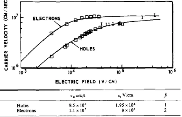
Chapter 4 Ballistic Efficiency in the Velocity Saturation Regime 56 4.1 The Equations in the Velocity Saturation Regime 56 4.1.1 The Empirical Equation 56 4.1.2 Modified Velocity Saturation Model 57
4.2 Ballistic Efficiency with the Velocity Saturation Properties 60 4.2.1 The Derivation of Id Equation in the Velocity Saturation
Regime
60
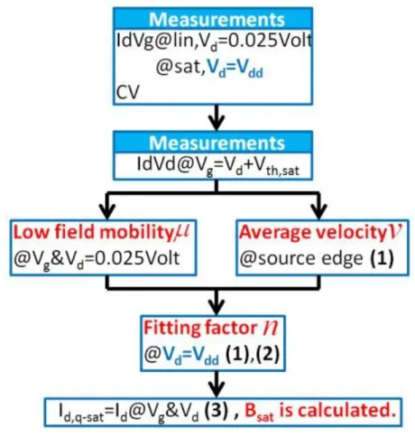
4.2.2 The Procedure to Determine Bsat by VSM Method 62
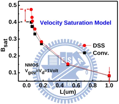
4.3 Experimental Results 63
4.3.1 The Comparison with TDM 63 4.3.2 Applications to Strained-Si Devices 66
Chapter 5 Conclusions 80
vii
Figure Captions
Fig. 2.1 (a) TEM graph of SBMOS and (b) schematic structure of conventional
MOSFET and SBMOS.
Fig. 2.2 The schematic process flow of SBMOS fabrication.
Fig. 2.3 (a) The band diagram on the varied state of operation in p-type SBMOS.
(b) The Id-Vd characteristic at on-state.
Fig. 2.4 (a) The band diagram on the varied state of operation in n-type SBMOS.
(b) The Id-Vd and Id-Vg characteristics at on-state.
Fig. 2.5 (a)TEM graph of DSS. (b) Band diagram of n-type DSS, and the dash
line represents that of SBMOS.
Fig. 2.6 The schematic process flow in DSS fabrication.
Fig. 2.7 (a) The SIMS profile of doping distribution under snowplow effect. (b)
The performance of DSS comparing with SBMOS. (c) The difference of
band diagram between DSS and SBMOS.
Fig. 2.8 DSS exhibits (a) better immunity of the short channel effect, (b) DIBL
characteristic and (c) series source/drain resistance than conventional
MOSFET.
Fig. 2.9 DSS shows higher Ion/Ioff ratio than conventional MOSFET.
Fig. 2.10 (a) The enhancement of velocity in DSS in comparison to the
conventional MOSFET which increases with reducing channel length.
(b) DSS shows more significant behavior of velocity overshoot than
conventional MOSFET.
Fig. 2.11 (a) The TEM graph of n-type DSS for our experiments. (b) The
viii
UMC.
Fig. 2.12 The experimental system of current-voltage (I-V) for both n-type and
p-type MOSFETs.
Fig. 2.13 DSS shows the better immunity to short channel effect and the lower
series source/drain resistance than conventional MOSFET one.
Fig. 2.14 Ion/Ioff ratio of DSS shows 11% enhancement over conventional
MOSFET.
Fig. 2.15 Id-Vd characteristics of (a) conventional MOSFET and (b) DSS.
Fig. 2.16 (a) Id-Vd characteristic of DSS comparing to conventional MOSFET, and
(b) DSS shows strong enhancement under short channel regime.
Fig. 2.17 Vdsat is defined by linear extrapolation to x-axis from gd-Vd curve.
Fig. 2.18 (a) gd-Vd characteristics of conventional MOSFET and DSS.
(b) Vdsat of DSS shows larger value than that of conventional MOSFET.
Fig. 2.19 Band diagram of the channel along the lateral direction.
Fig. 2.20 The plot of high field velocity versus low field mobility at fixed Vgov
Fig. 2.21 Channel band diagrams of DSS operating at (a) low field and (b) high
field.
Fig. 3.1 (a) The two-section model for backscattering theory. (b) The schematic
graph of carrier transport in the lateral band diagram.
Fig. 3.2 (a) The result of simulation and (b) that of approximate equation on vinj
versus surface density.
Fig. 3.3 The relation between Id current and temperature is used for TDM.
Fig. 3.4 The Bsat and rc in conventional MOSFET at L= 65nm are calculated by
ix
Fig. 3.5 The related parameters are calculated by TDM. (a) vinj. (b) rc. (c) . Fig. 3.6 Bsat versus temperature in conventional MOSFET in the range of (a)
55nm to 70nm and (b) 0.1um to 1um.
Fig. 3.7 Bsat versus temperature in DSS in the range of (a) 55nm to 70nm and (b)
0.1um to 1um.
Fig. 3.8 The result of Bsat versus channel length in DSS and conventional
MOSDET, which is calculated by TDM.
Fig. 3.9 The ratio of mean-free-path and critical length in conventional MOSFET
in the range of (a) 55nm to 70nm and (b) 0.1um to 1um.
Fig. 3.10 The ratio of mean-free-path and critical length in DSS in the range of (a)
55nm to 70nm and (b) 0.1um to 1um.
Fig. 3.11 The result of the mean-free-path versus channel length in DSS and
conventional MOSFET, calculated by TDM.
Fig. 3.12 The result of vinj versus channel length in DSS and conventional
MOSFET, calculated by TDM.
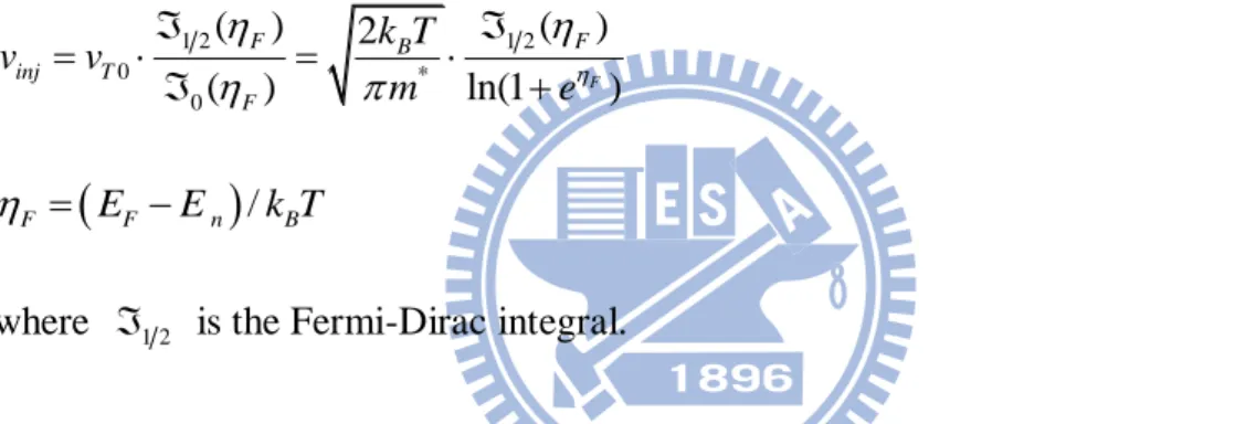
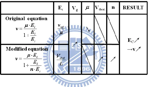
Fig. 4.1 The curve of carrier velocity with respect to electric field and the
empirical equation is applied on the plot.
Fig. 4.2 The comparisons between the original and the modified velocity
saturation equation for a varying Vg.
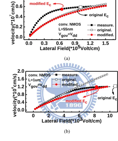
Fig. 4.3 The curve of carrier velocity in calculated by measurement comparing to
the original velocity model and the modified velocity model in (a) short
channel region and (b) long channel region.
Fig. 4.4 The plot of Vdsat versus channel length with respect to DSS and
x
Fig. 4.5 (a) The orientation of coordinates in the MOSFET device. (b) The
rearrangement of equations applied in the VSM.
Fig. 4.6 The procedure of using VSM to calculate Bsat.
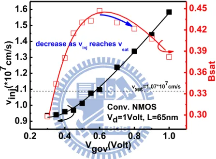
Fig. 4.7 The relation of vinj and Bsat with a varying Vgov.
Fig. 4.8 The Bsat is calculated by the VSM with respect to channel length.
Fig. 4.9 The vinj calculated by VSM in comparison to that by TDM.
Fig. 4.10 (a) The mean-free-path and (b) the critical field are calculated by VSM
in comparison to TDM.
Fig. 4.11 The comparison of carrier transport behavior in the channel between
conventional MOSFET and DSS.
Fig. 4.12 (a) The rule needs to be obeyed at a fixed Vgov. (b) The extreme value of
Bsat, which is defined by Bf, is calculated by VSM.
Fig. 4.13 The CESL type strained-si device is added for discussion about the vinj
and the Bsat.
1
Chapter 1
Introduction
1.1 Motivation
In the development of modern VLSI devices, many typical structures are
investigated for the enhancement of performance. For example, the strained-Si device
with SiGe S/D or CESL and high-k/metal gate stack were manufactured in the past
decade. They improved the loss of performance, which is induced by short channel
effect. The Schottky Barrier MOSFET (SBMOS) is another solution for metal silicide
replacing source and drain. It shows good ability on suppressing the short channel
effect, and has lower subthreshold swing which induces high Ion/Ioff ratio, but the
SBMOS has poor performance because the Schottky barrier height at silicide/channel
interface suppresses the transport efficiency of the carrier. This drawback limits the
development of SBMOS. In recent years, Tsui et al. [1.1] has provided an available
solution for improving performance through the additive process, called Dopant
Segregation implantation, being applied prior to the process of source/drain
silicidation. The Dopant Segregation (DS) layer is formed at silicide/channel interface,
and exhibits the quite high doping concentration. This is called the snowplow effect.
This SBMOS with DS layer is termed Dopant-Segregated SBMOS (DSS). The
addition of DS layer has succeeded in lowering and narrowing Schottky barrier, and
thus raised up the performance. Moreover, low series source/drain resistance induced
by modifying Schottky barrier has also been observed.
At present, high velocity over conventional MOSFET has been observed [1.2].
The high velocity leads the high performance. This behavior explained that DSS has
2
But the velocity overshoot phenomenon can not provide us a complete and detailed
analysis. Thus, we will use the ballistic theory to discuss the enhancement of velocity
as channel length is decreased, and develop a new approach called Velocity Saturation
Model (VSM) for the extraction of ballistic efficiency (Bsat) and injection velocity
(vinj). The higher Bsat and vinj, the better performance does. As a result, the VSM
provides us a good criterion for the analysis of performance enhancement.
1.2 Organization of the Thesis
This thesis was focused on analysis of transport efficiency in DSS, but we still
start from the basic properties. In Chapter 2, we introduce the basic properties of
SBMOS including structure, process flow and operating principle. Afterwards, the
improvement of DSS in comparison to the SBMOS is demonstrated and discussed.
In Chapter 3, the ballistic theory is introduced. We simply describe the origin of
principle and the Temperature Dependent Method (TDM) which is commonly used to
determinate Bsat. After that we use TDM to discuss the transport efficiency of DSS. In
Chapter 4, the VSM has been proposed in detail. The experimental results of DSS by
VSM comparing with those of TDM are also discussed. Finally, the conclusions are
Chapter 2
Performance of Schottky Barrier MOSFET
The Schottky Barrier MOSFET (SBMOS) is formed by metal silicide replacing
source/drain in conventional MOSFET. The hetero-junction at silicide/channel
interface determines the properties of SBMOS. In this chapter, we first introduce the
basic properties of SBMOS. And then, the Dopant-Segregated SBMOS (DSS) as a
key issue will be discussed.
2.1 Basic Properties of Schottky Barrier MOSFET
2.1.1 Device Structure and Process flow
In 1966, Nishi, first proposed a Japanese patent of SBMOS, but the first paper
for SBMOS is published by Lepselter and Sze, who are the well-known scholars in
semiconductor technology [2.1]. This is the first record of PtSi silicide PMOSFET. At
that time, SBMOS performed poor performance so that it did not receive much
attention. Later in 1984, T. Mochizuki and K. Wise reported a NMOSFET with
Schottky source/drain. This device improved the poor performance. Afterwards, the
SBMOS attracts much more attention. Several advantages of the SBMOS had been
reported repeatedly in the later years as the following:
1. Better for devices scaling down.
2. Low temperature processing for source/drain formation.
3. Better control of short channel effect.
5. Reduced the latch-up susceptibility.
A cross section TEM of SBMOS and schematic structure of conventional
MOSFET and SBMOS are shown in Figs. 2.1 (a) and (b). The main difference of
SBMOS with conventional MOSFET is that metal silicide replaces source/drain of
conventional MOSFET. The manufacturing process for SBMOS is simpler than
conventional MOSFET and fully compatible with the standard CMOS process.
The schematic process flow for the fabrication of SBMOS is shown in Fig. 2.2.
The process starts with a standard isolation process such as STI or LOCOS. Then, the
well implantation is applied to adjust Vth. Standard lithography and etch technologies
are used to form the gate stack, even the novel structures of gate stack such as
dual-polysilicon and metal gate/high-k could be applied to SBMOS. A thin sidewall
spacer formation is used to define the active operating region. Halo pocket
implantation is not necessary because of effective effect of Schottky source/drain
barrier controlling short channel effect well. The source/drain extension and deep
source/drain implantation are also eliminated.
During the process of silicidation, a dual-silicide exclusion-mask process is used
to form source/drain. No mask means that gate stack is treated as hard mask to be
patterned for definition of source/drain region. ErSi and PtSi are usually used to form
source/drain for n-type and p-type SBMOS respectively. Erbium and Platinum are
provided by standard PVD process equipment. During the cycle of thermal
silicidation, temperature is very important to be controlled. To avoid breaking active
region of device, the maximum temperature required for silicide reaction is less than
2.1.2 Principles of Operation
Although SBMOS has a similar structure with conventional MOSFET, SBMOS
exhibits different transport behaviors in operation. Figs. 2.3 and 2.4 show the band
diagrams on varied states of operation in p-type and n-type SBMOS respectively. The
carrier transport of p-type SBMOS relies on holes injecting into channel at the
valence band side, and that of n-type SBMOS relies on electrons injecting into
channel at the conduction band side. We consider p-type SBMOS as our discussion in
operation.
In Fig. 2.3 (a), we clearly see the difference of band diagram between SBMOS
and conventional MOSFET. At the channel edge, SBMOS has a significant barrier,
but conventional MOSFET doesn’t. At off-state, with Vg applied to 0 volt, the channel
barrier raises and stops the carrier transport at the valence band side. But there are still
some leakage carrier transporting through the channel on the other side, which means
conduction band side for p-type MOSFET. We can clearly understand that the
Schottky barrier in SBMOS makes the extra barrier preventing a large number of
leakage carrier entering the source. As a result, the Ioff current on off-state in SBMOS
has less magnitude than conventional MOSFET one.
When Vg increases over threshold voltage, the operation of device will be at
on-state. A large number of carriers enter the channel and reach to the drain, thus the
Id current raises strongly. In SBMOS, the Schottky barrier at source edge can’t make
carrier easily pass by. Comparing with conventional MOSFET, the SBMOS should
demonstrate less Id current than conventional MOSFET at on-state. Figs. 2.3 (b) and
Fig. 2.4 (b) show that SBMOS has weak Id current in both n-type and p-type SBMOS.
The loss of performance is due to Schottky barrier at the source edge. In spite of
on-state. This weakness limits the development of SBMOS, therefore finding a
method to enhance the performance of SBMOS is an important course for the
development.
2.2 SBMOS with Dopant Segregation Implantation
2.2.1 Device Structure and Process flow
In order to improve performance of SBMOS, many methods are investigated to
modify Schottky barrier at silicide/channel interface. One of available methods is the
addition of dopant segregation implantation prior to silicidation. This device is termed
as Dopant-Segregated SBMOS (DSS). The TEM graph of DSS is shown in Fig. 2.5
(a). It clearly shows the formation of Dopant Segregation (DS) layer at the
silicide/channel interface. Due to the addition of DS layer, the band diagram of
SBMOS is modified, as shown in Fig. 2.5 (b). The dash line represents the original
band diagram of SBMOS, which shows a higher barrier than DSS at silicide/channel
interface. The DS layer makes Schottky barrier lower and narrow, and the carrier at
the source side can pass the Schottky barrier easily. This behavior results in the
enhancement of Id current at on-state.
Figure 2.6 shows the schematic process flow of DSS from Toshiba. After
isolation formation, gate stack is formed by presented technologies, lithography,
thermal oxidation, deposition, and anisotropic etching. The process of DSS is also
compatible with standard CMOS techniques, after that, a disposable spacer sidewall is
formed to define the active region. After deep source/drain implantation, disposable
spacer is removed and Offset spacer is deposited. The use of halo implantation
Then, dopant segregation implantation and thermal process for silicidation are applied
to form DS layer. Finally, a complete device is formed after back-end process.
The DS layer is formed by the snowplow effect, which makes dopant redistribute
during thermal cycle of silicidation. Whether dopant redistribution occurs or not is
determined by diffusivity and solid solubility of dopant in the silicide and the
presence of dopant defects at silicide/si interface. In the case of NiSi phase, Ni atoms
are the moving species, supplied by diffusion through the growing silicide layer to
Si/Si interface because the covalent bonds between Si atoms are softened by diffusion
of Ni atoms. A significant change of volume is involved when silicide is formed. As a
result, point defects will be generated in order to partially relieve this stress. Due to
the formation of vacancies, the diffusivity of dopant in Si is enhanced and dopants
move toward the interface where it piles up between Si and Si. In case of dopant
segregation during silicidation, the high density of point defects can lead to a local
dopant concentration higher than solid solubility. The SIMS profiles after
redistribution of dopant are shown in Fig. 2.7 (a). A large number of dopants
concentrated at silicide/Si interface are observed.
2.2.2 The Comparisons with SBMOS
The addition of DS layer enhances the efficiency of carrier transport, which can
be understood in previous section. The Id-Vd characteristic of DSS and the
comparison with SBMOS is shown in Fig. 2.7 (b). The performance of DSS shows
the significant enhancement, and the leakage current of DSS lower than conventional
MOSFET is observed. We can make comparisons of the band diagram in both two
devices, as shown in Fig. 2.7 (c).
the hole tries to enter channel, and reaches to the source. The decrease of leakage
current by Schottky barrier in valence band formed at drain edge is clearly
demonstrated in SBMOS. However, the DSS shows higher Schottky barrier height in
valence band than SBMOS, which induces the stronger suppression on leakage
current than SBMOS. Consequently, the Ioff of DSS is lower than that of SBMOS.
At on-state, the electrons are injected into the channel, and are collected by the
drain. In SBMOS, the Schottky barrier at source edge at conduction band blocks a
large number of electron entering channels. In DSS, the DS layer modifies the
Schottky barrier at silicide /channel interface shown in Fig. 2.5 (b). The narrower and
lower Schottky barrier thickness and height is generated. Based on quantum effect,
the narrower and lower barrier thickness and height enhance the probability of particle
tunneling. Consequently, the electron can enter channel by tunneling through Schottky
barrier at present. This extra carrier injection raises the performance up, and the
performance of DSS shows better result than SBMOS practically.
2.2.3 Advantages of DSS
The performance enhancement by the addition of DS layer in SBMOS is shown
in the previous section. Hence, we will show the other advantages in the use of DSS.
Fig. 2.8 (a) and Fig. 2.8 (b) show that DSS has better immunity to suppress the short
channel effect and DIBL characteristic than conventional MOSFET. As channel
length scaling down, these can make the device more stabilized. Furthermore, the
series source/drain resistance of DSS less than conventional MOSFET is also
observed through the Rtot-Vd curve, as shown in Fig. 2.8 (c). This is because DS layer
modifies the Schottky barrier at silicide/channel interface, the contact resistance
one of the reasons enhances the performance of DSS.
Figure 2.9 shows that the Ion/Ioff ratio of DSS is larger than conventional
MOSFET. This result corresponds to better performance and lower series source/drain
resistance than conventional MOSFET before. For the discussion on performance, the
carrier velocity is used for further study. A. Kinoshita first proposes that DSS has the
more significant behavior of velocity overshoot in IEDM 2006 [1.2]. Fig. 2.10 (a) and
Fig. 2.10 (b) show his experimental results. As channel length scaling down, the
difference of velocity in DSS comparing with conventional MOSFET increases
strongly. We can see that the velocity in DSS overshoots over saturated velocity (vsat)
in the short channel regime. The experimental results provide us an explanation for
the performance enhancement, but there is still not a series of complete and detailed
discussion. We will discuss it through the ballistic theory in the next chapter.
2.3 Device Preparation and Experimental Setup
2.3.1 Device Preparation
For our experiments, the experimental devices and control devices are needed to
be verified clearly. The devices are based on 65nm technology of United
Microelectronics Corporation (UMC) in Taiwan. Fig. 2.11 (a) shows the TEM
cross-section image of DSS, and Fig. 2.11 (b) depicts the schematic process flow for
fabrication. The channel length ranges from 55nm to 1um with width varying from
70nm to 1um, and the largest device with W/L= 10um/10um is used for measurement
in capacitance of gate dielectric. The code name LO65-BSRx (x: 1~ c) devices are
used for major measurements of characteristic analysis. The pieces of wafer named
In the fabrication, the STI isolation is formed first, and so is gate stack with
1.2nm thickness of gate dielectric. The offset spacer is used to define active region.
Halo and dopant segregation implantation are applied prior to the formation of
disposable spacer which defines source/drain. After disposable is removed, metal
silicide (NiPtSi) is formed during thermal cycle of silicidation. Temperature RTP
lower than 600 oC is applied to avoid destroying device.
2.3.2 Experimental Setup
The experimental setup for the current-voltage measurement of devices is
illustrated in Fig. 2.12. Both intrinsic and degradation behaviors of the devices can be
achieved by this system. Each of the analyzers is connected by the co-axial or tri-axial
cable including the semiconductor parameter analyzer (HP 4156C), the low leakage
switch mainframe (HP E5250A), the Cascade guarded thermal probe station, and a
thermal controller. This facility provides an adequate capability for measuring the low
leakage devices I-V characteristic. On the other hand, for precisely measuring of
capacitance-voltage characteristic of the devices, LCR Meter (Agilent-HP 4284A) has
been added. It provides the testing frequency from 20Hz to 1MHz for AC voltage.
These analyzers are controlled by the corresponding software in PC. Therefore, our
group developed a control system in HT-Basic language. Through IEEE-488 (GPIB)
cable, we can directly give the order to each analyzer. From the above system, the I-V
2.4 The Discussions of DSS on Performance
2.4.1 Basic Characteristics
The better immunity and lower series source/drain resistance of DSS against
conventional MOSFET are shown in Fig. 2.13 (a) and Fig. 2.13 (b), respectively. Fig.
2.14 shows that the Ion/Ioff ratio of DSS provides enhancement of +11% over
conventional MOSFET. Fig. 2.15 shows the Id-Vd characteristics of conventional
MOSFET and DSS with channel length ranging from 1um to 55nm. In Fig. 2.16, we
can clearly see that the Id current of DSS demonstrates the enhancement of +15.2% at
L= 55nm. Besides, it can significantly be seen that the performance enhancement
increases with decreasing channel length. As channel length is down to 0.2um, the
enhancement begins to rise rapidly.
The conductance, gd, is the differential of Id with respect to Vd. It can be seen as
the ability of lifting up Id with the variation of Vd. Besides, the gd-Vd curve can be
used to define the Vdsat, which means the onset of entering saturation region. When Vd
reaches Vdsat, the Id current gradually tends to saturation, and Id current doesn’t
increase rapidly. As a result, the higher Vdsat leads to the later onset of entering
saturation region, and Id current could lift up more highly. In Fig. 2.17, the Vdsat is
defined by linear extrapolation to x-axis on the gd-Vd plot.
Figures 2.18 (a) and (b) show the gd-Vd characteristic of DSS against
conventional MOSFET. DSS demonstrates higher gd at all of ranges and higher Vdsat
than conventional MOSFET. Consequently, DSS will have a better performance than
conventional MOSFET. We can analyze the band diagram in the lateral direction to
explain these results. Since the DS layer is added, the Schottky barrier with abrupt
into high energy level state, and thus the transport efficiency will be improved. After
carrier entering channel, the high energy state expands the difference between the
carrier and the bottom of conduction band. Because of the increasing difference, it
will succeed in overcoming the part of scattering mechanism induced by lattice
vibration. Therefore, the carrier can pass channel by more easily, and Id current is late
for entering saturation region. As a result, DSS exhibits higher gd and Vdsat than
conventional MOSFET.
2.4.2 Analysis on Transport Efficiency
Since the low field mobility decreases seriously at high field, it is commonly
believed as the limitation of saturated velocity. In IEDM 2006 [2.2], M. Saitoh
utilizes the fixed Vg, Vd and Vdsat to maintain the same channel potential profile for
inspection of the relation between low field mobility and high field velocity. We also
use this experimental setup to observe the difference of the device performance.
As Vd reaches Vdsat, the Id current goes into saturation region, which is termed
pinch-off. When Vd continues to increase, the pinch-off point will slide toward the
direction of the source, and the increased bias Δ Vd, which is equal to Vd-Vdsat, will
be applied near drain edge densely. Since the pinch-off occurs, the Id gain beyond
pinch-off with the variation of Δ Vd can be seen as transport efficiency under
saturation regime. The scheme is shown in Fig. 2.19.
As mentioned in the previous paragraph, Vdsat is a critical parameter to determine
Id. Hence, we could fix Vdsat and Vgov for estimations of performance between DSS
and conventional MOSFET. In Fig. 2.20, high field velocity against low field mobility
is plotted at fixed Vgov. Exactly, low field mobility is a function of vertical field ( refer
same mobility can be considered to be the same condition of band bending in the
channel, which means at the same Vdsat. This plot shows these two curve have more
significant split with decreasing channel length, but the difference of mobility retains
a nearly range.
We can utilize channel band diagram of DSS in lateral direction shown in Fig.
2.21 to explain the discrepancy. At low field, low Vd is applied in the lateral direction
which is too small to not help plenty carrier climb over the Schottky barrier, the
transport mechanism at Schottky barrier interface is dominated by the tunneling. Thus
a little part of carrier overcomes barrier height and goes into high energy state to
enhance mobility at low field. As Vd increases into high field regime, a large number
of carrier travels easily over Schottky barrier, and then enters channel. The carrier has
enough energy to transport through channel, it is considered that the probability of
transporting into drain should be larger as channel length decreases due to lower
scattering impact. As a result, the difference of high field velocity with respect to DSS
and conventional MOSFET increases with decreasing channel length. This
enhancement of the velocity will be discussed by ballistic theory in the next two
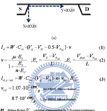
(a)
(b)
Fig.2.1 (a) TEM graph of SBMOS and (b) schematic structure of
(a)
(b)
Fig.2.3 (a) The band diagram on the varied state of operation in p-type
(a)
(b)
Fig.2.4 (a) The band diagram on the varied state of operation in n-type
(a)
(b)
Fig.2.5 (a)TEM graph of DSS. (b) Band diagram of n-type DSS, and the
(a)
(b)
(c)
Fig.2.7 (a) The SIMS profile of doping distribution under snowplow
effect. (b) The performance of DSS comparing with SBMOS.
(a)
(b)
(c)
Fig.2.8 DSS exhibits (a) better immunity of the short channel effect, (b)
DIBL characteristic and (c) series source/drain resistance than
(a)
(b)
Fig.2.10 (a) The enhancement of velocity in DSS in comparison to the
conventional MOSFET which increases with reducing channel
length. (b) DSS shows more significant behavior of velocity
(a)
(b)
Fig.2.11 (a) The TEM graph of n-type DSS for our experiments. (b) The
schematic process flow of DSS based on 65nm technology node
Fig.2.12 The experimental system of current-voltage (I-V) for both
n-type or p-type MOSFET. Cascade Guarded
Thermal Probe Station
Personal Computer Thermal Controller HP 8110A Pulse Generator Switch Matrix HP 5250A Parameter Analyzer HP 4156
0.06 0.09 0.12 0.15 0.18 0.24 0.28 0.32 0.36 0.40 0.44 0.48 DSS Conv. Vth (V o lt ) L(um) NMOS @lin,Vd=0.025Volt (a) 0.00 0.04 0.08 0.12 0.16 200 300 400 500 600 700 DSS Conv. NMOS Vg=1Volt Rto t( *1 0 -3 o h m -u m ) L(um) (b)
Fig.2.13 DSS shows the better immunity to short channel effect and the
lower series source/drain resistance than conventional MOSFET
600
800
1000
1200
1E-9
1E-8
1E-7
1E-6
1E-5
Conv.
DSS
I off (A /u m )Ion(A/um)
+11%
Fig.2.14 Ion/Ioff ratio of DSS shows 11% enhancement over conventional
MOSFET.
(a)
(b)
Fig.2.15 Id-Vd characteristics of (a) conventional MOSFET and (b) DSS.
0.0 0.2 0.4 0.6 0.8 1.0 0.0 0.2 0.4 0.6 0.8 1.0 I d (m A /u m ) Vd(Volt) 55nm 60nm 65nm 70nm 0.1um 0.18um 0.5um 1um Conv. MOS Vg=1+Vth,sat @25oC 0.0 0.2 0.4 0.6 0.8 1.0 0.0 0.2 0.4 0.6 0.8 1.0 DSS Vg=1+Vth,sat @25oC 55nm 60nm 65nm 70nm 0.1um 0.18um 0.5um 1um I d (m A /u m ) Vd(Volt)
0.0
0.2
0.4
0.6
0.8
1.0
0.0
0.2
0.4
0.6
0.8
1.0
DSS Conv.+15.2%
I d (m A /u m )Vd(Volt)
NMOS Vgov=1Volt L=1.0um~55nm (a) 0.0 0.2 0.4 0.6 0.8 1.0 0 3 6 9 12 15 I d G a in (% ) L(um) strong increase DSS Current Gain against Conv. Vgov=1Volt L=1.0um~55nm (b)Fig.2.16 (a) Id-Vd characteristic of DSS comparing to conventional
MOSFET, and (b) DSS shows strong enhancement under short
0.0
0.2
0.4
0.6
0.8
1.0
0.0
0.5
1.0
1.5
2.0
2.5
3.0
g d (* 1 0 -3 A /V o lt -u m )V
d(Volt)
increasing Vglinear extrapolation
to define Vdsat
Conv. NMOS, L=55nm
Vg=1.0~1.25Volt
Step=0.05Volt
Fig.2.17 Vdsat is defined by linear extrapolation to x-axis from gd-Vd
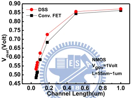
(a) 0.0 0.2 0.4 0.6 0.8 1.0 0.45 0.50 0.55 0.60 0.65 0.70 0.75 0.80 0.85 0.90 NMOS Vgov=1Volt L=55nm~1um V ds a t (V o lt ) Channel Length(um) DSS Conv. (b)
Fig.2.18 (a) gd-Vd characteristics of conventional MOSFET and DSS. (b)
Vdsat of DSS shows larger value than that of conventional
MOSFET. 0.0 0.2 0.4 0.6 0.8 1.0 0.0 0.5 1.0 1.5 2.0 2.5 3.0 DSS Conv. gd (m A /V o lt -u m ) Vd(Volt) NMOS Vgov=1Volt L=55nm
Fig.2.20 The plot of high field velocity versus low field mobility at fixed Vgov. 100 125 150 175 200 225 250 1 2 3 4 5 6 7 8 long channel DSS Conv. v e lo c it y (* 1 0 6 c m /s ) mobility(cm2/Volt-s) NMOS Vgov=1Volt L=55nm~1um v@Vd=1Volt @Vd=0.025Volt short channel
(a)
(b)
Fig.2.21 Channel band diagrams of DSS operated at (a) low field and (b)
Chapter 3
Fundamentals of Ballistic Transport Theory
Semiconductor devices have been scaled down to the nano-scale region, and
entered the quasi-ballistic regime. Because of the physical limitations of carrier
transport, the drift-diffusion model for describing carrier transport becomes less
significant in the nano-scale MOSFET. From the quasi-ballistic toward ballistic
region, Natori brought up a new insight for modeling the carrier transport
phenomenon, which is called ballistic theory or backscattering theory in 1994 [3.1].
Later in 1997, Lundstrom developed the complete theorem to explain the physical
meaning of the ballistic transport phenomenon in nano-scale MOSFET [3.2].
3.1 Introduction of Ballistic Theory
3.1.1 Backscattering Principle and Current Transport Model
In ballistic theory, we treat the moving carriers as the quantum wave. This kind
of wave goes through channel from the source to the drain. When the waves move
toward the channel, they bomb into a non-negligible quantum barrier which leads to
transmission and reflection in quantum mechanics. In saturation region of MOSFET,
the channel barrier is like the shape of hills. The length is called critical length,
which means the potential drops kBT from the edge of source to channel, where
B
k is the Boltzmann constant and T is the temperature in Kelvin coordinates. In the
critical length, the carrier suffers from strong resistance induced by the scattering
mechanism. Thus, the longer results in the carrier suffers from the stronger
impurity scattering, lattice vibration, and surface roughness. The mean-free-path of carrier in the channel means the expected length of carrier transporting through
channel. The longer responds to the better transport efficiency. As a result, when the carrier enters channel, the probability of reaching drain is determined by the
relation of and . We can define the backscattering coefficient r , in which the c
probability of the carrier bounced back to source, as following:
1 1 c r (3.1)
On the other hand, it also can be represented the probability of the carrier passing
through channel. The ballistic efficiency, which called Bsat is given by: 1 1 c sat c r B r (3.2)
In 1997, Lundstrom presented a simple scattering model based on the ballistic
theory for carrier transport. Under the operation, the two-section model is shown in
Fig. 3.1 (a). The source is treated as a reservoir of carriers which injects a flux as into
the channel, and the flux aD represents the carriers which succeeded to be collected by
drain. We can more clearly see the mechanism of carrier transport in Fig. 3.1 (b).
The fraction ts means the source flux which transmits across the barrier at
source/channel interface, and enters the channel. The fraction tc of flux, which injects
into the channel, and exists in drain, represents the transport efficiency of carrier.
Thus, the fraction rc, which means the backscattering coefficient, is defined as rc= 1- tc.
The flux as before injecting into channel can be written by:
(0) (0, )
s inj
a n z v (3.3)
where vinj is the injection velocity in the lateral direction and n is the density of carrier
in the source reservoir. Then, the Eq. 3.3 links up ts and rc, and we can rearrange the
(0)
s s s s s c
a a t a t r (3.4)
1 tc rc (3.5)
Through the transmission of fraction tc, aD can be represented by:
D s s c
a a t t (3.6) Substituting Eq. 3.4 and Eq. 3.5 into Eq. 3.6, and integrating aD with respect to the
channel width. We can obtain the Id equation under the ballistic theory.
0 1 ( ) 1 W c d D ox g th inj c r I q W a dz W C V V v r
(3.7)The Id equation also can be written as:
( )
d ox g th inj sat
I W C V V v B (3.8)
This equation represents the transport efficiency of carrier in the channel, which
provides us a simple current expression without invoking the unpredictable mobility.
In the ultimate of ballistic theory, the Bsat tends to 1 and Id will be fully controlled by
3.1.2 Injection Velocity
The maximum value of velocity under classical thermal equilibrium is simply
defined as thermal velocity, 0 2 B* T
k T v
m
. The random velocity can exceed this thermal limit due to quantum mechanism effect, and this behavior is induced by
degeneracy of carrier. Thus, the average carrier energy is triggered to the high energy
state, and the carrier will have higher velocity than thermal velocity. The ballistic
theory assumes the thermal velocity on carrier degeneracy to be the injection velocity
(vinj). As a result, the vinj is given by:
1 2 1 2 0 * 0 ( ) 2 ( ) ( ) ln(1 F) F B F inj T F k T v v m e (3.8)
/ F EF En k TB (3.9)where 1 2 is the Fermi-Dirac integral.
When the operation is in the weak inversion, Eq. 3.8 is reduced to vinj vT0. The simulation result of Eq. 3.8, considering the occupation of single valley in band
structure, is shown in Fig. 3.2 (a). The vinj demonstrates the significant trend with
respect to the surface density. When gate bias continues to increase beyond the
threshold voltage, the strong accumulation of inversion charge will raise surface
density up. As a result, the behavior, which vinj exceeds vT0, is observed.
Besides, we have found another approximate equation for expressing the vinj
under the state of degeneracy. The equation is given by:
* ( ) 8 3 2 ox g th inj C V V v m q (3.10)
3.2 Ballistic Efficiency with Temperature Dependent Properties
3.2.1 Temperature Dependent Parameters
The ratio of and is the important element for determination of Bsat, and is a function of temperature. From Eq. 3.8, we can see that the vinj is also dependent on
temperature. Thus, Chen developed a model with respect to temperature for
calculating rc or Bsat [3.3]. Through rearranging Eq. 3.1 and Eq. 3.7, the Id equation
can be rewritten by:
( ) 2 d ox g th inj I W C V V v (3.11) where 2 is equal to Bsat.
In Eq. 3.11, there are several parameters which are related to temperature, and we list
those below.
1. Injection velocity, vinj
1 1 2 2 * ( ) 2 ln(1 F) F B inj k T v T m e (3.12) 2. Critical length, B d k T L T q V (3.13)
where L is channel length.
3. mean-free-path,
At first, we need to know the relation between vinj and . This relation can be derived from the Einstein relation, and is given by:
0 2 B inj k T q v (3.14)
And, the 0 is also a function of temperature.
1.5 0 T
(3.14)
As a result, we have found the relation with respect to temperature.
1 0 2 B inj k T q T v (3.15) 4. threshold voltage, Vth
The relation of Vth and temperature will be calculated by the practical measurements.
3.2.2 Derivation and Application of Temperature Dependent Current Equation
Eq. 3.12, Eq. 3.13, Eq. 3.15 and Vth(T) are replaced in Eq. 3.11, and we
differentiate Id equation with respect to temperature.
2 1 1 2 d T d g th T g th I v I V V T v T T V V T
1 4 1 1 2 2 d d g th g th I I V V T T V V T (3.16)Then, Eq. 3.16 can be simplified as the following:
d d I I T (3.17)
And, we rearrange the equation from Eq. 3.16 and Eq. 3.17. The equation can be obtained as below. ( ) 1 0.5 g th g th g th V V T V V V V (3.18)
Afterward, the Eq. 3.17 and Eq. 3.18 will be used to calculate the Bsat and rc in
different devices, which is generally called Temperature Dependent Method (TDM).
In the beginning of using TDM, we need to calculate by measurements. Fig. 3.3 shows the relation of Id and T, and the parameter which means the slope of the
curve is calculated. Then, substitute into Eq. 3.18, we can find the ratio of and , and Bsat will be calculated through Eq. 3.11.
In the paper that Chen proposed, the Id equation with considering series
source/drain resistance can be rewritten by:
( 0.5 )
d ox g th d SD inj sat
I W C V V I R v B (3.19)
where Id RSD is the voltage consumption induced by series source/drain resistance. Figure 3.4 shows that the Bsat and rc in conventional MOSFET at L= 65nm are
calculated by TDM. As temperature increases, the Bsat decreases due to the strong
thermal scattering. Fig. 3.5 shows the results of vinj, rc and with respect to gate bias, which are calculated by TDM.
3.3 Experimental Results
3.3.1 Ballistic Efficiency
In this section, we use the TDM to calculate Bsat, the ballistic efficiency, and
compare the results of DSS with that of conventional MOSFET. Fig. 3.6 and Fig. 3.7
show the results of Bsat with respect to temperature in conventional MOSFET and
DSS, respectively. The same trend with increasing temperature, both devices
demonstrate the behavior of decreasing Bsat. But we also observe some values of Bsat
in conventional MOSFET at L= 1um is lower than 0. This means that all carriers
could not be injected into channel even on on-state operation. Actually, we have the
data of Id, which is greater than 0. Thus, the negative Bsat calculated by TDM is
observed, and we will discuss it in the next chapter.
conventional MOSFET. Fig. 3.8 provides us a more clear result of Bsat with respect to
channel length at the fixed temperature, and demonstrates that DSS has higher Bsat in
all range. At L= 1um, the Bsat difference between DSS and conventional MOSFET is
the highest, and the difference decreases with decreasing channel length.
3.3.2 The Ratio of Mean-Free-Path and Critical Length
The ratio is calculated by Eq. 3.11. Because the ratio is proportional to Bsat, we will obtain the result of versus channel length approaching that of Bsat versus channel length. Fig. 3.9 and Fig. 3.10 show the results of with respect to temperature in conventional MOSFET and DSS, respectively.
Moreover, we continues to calculate the estimated value of which is obtained by Eq. 3.14. In Eq. 3.14, there are two unknown parameters at present, which are 0 and vinj. The low field mobility 0 is calculated by gd method as shown below.
, d d lin ox g th V I W C V V L
, d lin d ox g th d I W g C V V V L
d ox g th g L W C V V (3.20)where Cox is the capacitance of gate dielectric which is estimated by split-CV
measurement. And through the Id equation, the vinj can be obtained after Bsat and Cox
are calculated.
Thus, versus channel length which is calculated by TDM will be obtained, as shown in Fig. 3.11. DSS demonstrates the higher value than conventional MOSFET
difference between DSS and conventional MOSFET is the largest. As channel length
decreases, the difference gradually disappears.
3.3.3 Injection Velocity
We can calculate vinj once Bsat and Cox are found. The vinj is treated as an
important performance criterion. From the Id equation, we understand that the higher
vinj may lead to higher Id. Besides, the vinj will dominate the Id current when Bsat
approaches one.
The result of vinj is shown in Fig. 3.12. We first look at the curve of conventional
MOSFET. The curve doesn’t show the uniform trend with respect to channel length.
We need to see the equation of vinj. In Eq. 3.12, we observe that the vinj is not a
function of channel length, and is only dependent on temperature, the effective mass
and the level of carrier degeneracy. This conclusion is consistent with the curve of
conventional MOSFET in our measurement.
Then, we see the curve of DSS. It was found that the curve is strongly dependent
on the channel length. When channel length decreases, the vinj has a significant trend
which is rising up. This point receives our attention because the abnormal trend of vinj
may be induced by the model errors in TDM. We suppose that one or two temperature
dependent models are not suitably applied in DSS, which results in the wrong vinj
estimation. Because of the model errors, the TDM can’t be applied to the case of DSS.
Thus, the estimations including Bsat, and vinj are needed to be calculated by another way.
(a)
(b)
Fig.3.1 (a) The two-section model for backscattering theory. (b) The
(a)
(b)
Fig.3.2 (a) The result of simulation and (b) that of approximate equation
Fig.3.3 The relation between Id current and temperature is used for TDM. 280 290 300 310 320 330 0.81 0.82 0.83 0.84 0.85 0.86 0.87 0.88 Id (m A /u m ) T(K) Conv. MOS L=65nm Vgov=Vd=1Volt
Fig.3.4 The Bsat and rc in conventional MOSFET at L= 65nm are calculated by TDM. 280 290 300 310 320 330 0.35 0.40 0.45 0.50 Conv. MOS L=65nm Vgov=Vd=1Volt rc Bsat T(K) r c 0.35 0.40 0.45 0.50 B s a t
(a)
(b)
(c)
Fig.3.5 The related parameters are calculated by TDM. (a) vinj. (b) rc.
(a)
(b)
Fig.3.6 Bsat versus temperature in conventional MOSFET in the range of
(a) 55nm to 70nm and (b) 0.1um to 1um.
10 20 30 40 50 60 0.44 0.46 0.48 0.50 0.52 B s a t T(oC) 55nm 60nm 65nm 70nm Conv. MOS Vgov=Vd=1Volt 10 20 30 40 50 60 -0.2 -0.1 0.0 0.1 0.2 0.3 0.4 0.5 0.6 Conv. MOS Vgov=Vd=1Volt B s a t T(oC) 0.1um 0.18um 0.5um 1um
(a)
(b)
Fig.3.7 Bsat versus temperature in DSS in the range of (a) 55nm to 70nm
and (b) 0.1um to 1um.
10 20 30 40 50 60 0.50 0.52 0.54 0.56 DSS Vgov=Vd=1Volt B s a t T(oC) 55nm 60nm 65nm 70nm 10 20 30 40 50 60 0.0 0.1 0.2 0.3 0.4 0.5 DSS Vgov=Vd=1Volt B s a t T(oC) 0.1um 0.18um 0.5um 1um
Fig.3.8 The result of Bsat versus channel length in DSS and conventional
MOSDET, which is calculated by TDM.
0.0 0.2 0.4 0.6 0.8 1.0 0.1 0.2 0.3 0.4 0.5 0.6 NMOS Vgov=Vd=1Volt @25oC B s a t L(um) Conv. MOS DSS
(a)
(b)
Fig.3.9 The ratio of mean-free-path and critical length in conventional
MOSFET in the range of (a) 55nm to 70nm and (b) 0.1um to
1um. 10 20 30 40 50 60 1.6 1.7 1.8 1.9 2.0 2.1 Conv. MOS Vgov=Vd=1Volt R a ti o o f m e a n -f re e -p a th t o c ri ti c a l le n g th T(oC) 55nm 60nm 65nm 70nm 10 20 30 40 50 60 -1.0 -0.5 0.0 0.5 1.0 1.5 2.0 Conv. MOS Vgov=Vd=1Volt R a ti o o f m e a n -f re e -p a th t o c ri ti c a l le n g th T(oC) 0.1um 0.18um 0.5um 1um
(a)
(b)
Fig.3.10 The ratio of mean-free-path and critical length in DSS in the
range of (a) 55nm to 70nm and (b) 0.1um to 1um.
10 20 30 40 50 60 2.0 2.1 2.2 2.3 2.4 2.5 2.6 DSS Vgov=Vd=1Volt R a ti o o f m e a n -f re e -p a th t o c ri ti c a l le n g th T(oC) 55nm 60nm 65nm 70nm 10 20 30 40 50 60 -1.0 -0.5 0.0 0.5 1.0 1.5 2.0 2.5 DSS Vgov=Vd=1Volt R a ti o o f m e a n -f re e -p a th t o c ri ti c a l le n g th T(oC) 0.1um 0.18um 0.5um 1um
Fig.3.11 The result of the mean-free-path versus channel length in DSS
and conventional MOSFET, calculated by TDM.
0.0 0.2 0.4 0.6 0.8 1.0 4 6 8 10 12 14 16 18 20 22 NMOS Vgov=Vd=1Volt @25oC m e a n -f re e -p a th (n m ) L(um) Conv. MOS DSS
Fig.3.12 The result of vinj versus channel length in DSS and conventional MOSFET, calculated by TDM. 0.0 0.2 0.4 0.6 0.8 1.0 0.6 0.8 1.0 1.2 1.4 NMOS Vgov=Vd=1Volt @25oC vin j( *1 0 7 c m /s ) L(um) Conv. MOS DSS