Defect-Enhanced Visible Electroluminescence
of Multi-Energy Silicon-Implanted
Silicon Dioxide Film
Chun-Jung Lin and Gong-Ru Lin, Senior Member, IEEE
Abstract—White-light and blue–green electroluminescence (EL) of a multirecipe Si-ion-implanted SiO2 (SiO2:Si+) film on Si substrate are demonstrated. The blue–green photoluminescence (PL) is enhanced by the reaction of O3 Si-O-Si O3 O3 Si-Si O3 + Ointerstitial during Si implantation. After annealing at 1100 C for 180 min, the luminescence at both 415 and 455 nm is markedly enhanced by the complete activation of radiative defects, such as weak oxygen bonds, neutral oxygen vacancies (NOVs), and the precur-sors of nanocrystallite Si ( centers). Absorption spectroscopy and electron paramagnetic resonance confirm the existence of NOVs and centers. The slowly rising -related PL intensity reveals that the formation of nanocrystallite Si (nc-Si) requires longer annealing times and suggests that the activation energy for diffusion of excess Si atoms is higher than that of other defects in ion implanted SiO2. The EL from the Ag–SiO2:Si+ -Si–Ag metal–oxide–semiconductor diode changes from deep blue to green as the driving current increase from 0.28 to 3 A. The max-imum white-light luminescent power is up to 120 nW at a bias current of 1.25 A.
Index Terms—Electroluminescence (EL), MOS diode,
photolu-minescence (PL), Si-ion implantation, Si-rich silicon dioxide.
I. INTRODUCTION
S
ILICON-RICH SiO materials can be synthesized by electron-beam evaporation [1], RF-magnetron sput-tering, Si-ion implantation [2], and plasma-enhanced chemical vapor deposition (PECVD) [3].. Previously, porous Si [4], PECVD-grown Si-rich SiO , amorphous Si:H:O, and Si-im-planted SiO SiO Si have been shown to exhibit photo-luminescence (PL) and electrophoto-luminescence (EL) spreading from blue–green to the near-infrared region (340–800 nm) [1], [5]–[9]. Particularly, the structural defects in the sil-icon-rich SiO responsible for visible PL at 400–500 nm have caused great interest [10]. Silicon implantation usually introduces versatile defects in SiO [11], for example, the neutral oxygen vacancy (NOV) and the nonbridging oxygen hole center (NBOHC) [6], [12], [13]. Some of the radiative defects such as NOV and NBOHC can be activated via appro-priate annealing processes. The contribution of NOV defects to the PL at 450–470 nm has been verified in previous reportsManuscript received August 16, 2004; revised November 29, 2004. This work was supported in part by the National Science Council of the Republic of China under Grant NSC93-2215-E-009-007 and Grant NSC92-2215-E-009-028.
The authors are with the Department of Photonics and the Institute of Electro-Optical Engineering, National Chiao Tung University, Hsinchu, Taiwan 300, R.O.C. (e-mail: [email protected]).
Digital Object Identifier 10.1109/JQE.2004.842314
Fig. 1. TRIM calculations for Si-ion implantation into 500-nm-thick SiO film with (a) 52 10 ions=cm at 40 keV, (b) 5 2 10 ions=cm at 80 keV, (c) 52 10 ions=cm at 150 keV, and (d) multirecipe of 5 2 10 ions=cm , 12 10 ions=cm , and 2 2 10 ions=cm .
[14]–[16], whereas the nanocrystallite Si (nc-Si) embedded in the annealed SiO Si matrix contributes to the emission at longer wavelengths [11]. Although two contradictory PL mechanisms exist, most studies focus on the nc-Si-correlated PL characteristics, while few studies have investigated the defect-induced blue–green PL. In this study, the luminescent centers in SiO Si before and after thermal annealing are characterized by absorption spectroscopy and electron para-magnetic resonance (EPR). The defect-enhanced EL from an SiO Si -based MOS diode and its corresponding mechanisms are reviewed.
II. EXPERIMENT
SiO Si samples were prepared by multi-energy Si-ion implantation into a 5000- -thick SiO film on 500- m-thick, (100)-oriented, n-type Si substrate with a resistivity of 4–7 cm. The SiO film was deposited by PECVD under mixed tetraethoxysilane (TEOS) and O with fluences of 10 and 200 sccm, respectively. The chamber pressure and power were 400 mTorr and 150 W, respectively. Si-implantation con-ditions were 5 10 ions cm at 40 keV, 1 10 ions cm at 80 keV, and 2 10 ions cm at 150 keV. This results in a uniformly distributed Si-implantation profile with a depth of 100 and 5000 below the sample surface, as calculated by the simulation program, “transport of ions in matter” (TRIM) [5], as shown in Fig. 1. Some samples were encapsulated and annealed at 1100 C in a quartz furnace tube under flowing
Fig. 2. PL spectra of the SiO:Si –Si samples at (a) as-implanted condition or annealed at 1100 C for (b) 30, (c) 60, (d) 180 and (e) 240 min. The inset figure plots the PL spectra of (1) n-type Si substrate, (2) 60-min annealed n-type Si substrate, (3) SiO –Si sample, (4) 60-min annealed SiO –Si sample, and (5) as-implanted substrate.
gas for times ranging from 15 to 300 min, in order to help activate radiative defects and to eliminate the carrier-trapping centers buried in the SiO –Si substrate. To excite photoelec-trons in the SiO Si sample for room-temperature and CW PL measurements, an He-Cd laser with a wavelength and an average intensity of 325 nm and 5 W/cm , respectively, were employed as the pumping source. The PL from 360 to 700 nm was resolved by a fluorescent spectrophotometer (Jobin Yvon, TRIAX-320) using a 1200-g/mm grating with a wavelength resolution of 0.06 nm and detected by a cooled photomulti-plier (Jobin Yvon, Model 1424M)-based photon counter. The working distance between the focusing lens and the sample was fine-tuned to maximize the PL intensity. A MOS diode was made by coating 500- -thick 2-mm silver contacts on the SiO Si /n-Si substrate. After metallization, a sintering process was performed at 150 C for 10 min in the ambient atmosphere. By using a pair of microprobes (Karr Suss, 253), the MOS diode was driven by either a pulsed current source (ILX, LDP-3840) or a voltage source meter (Keithley, 236). The pulsed current and the CW voltage were scanned from 0 V to 3 A and from 0 to 30 V, respectively. The optical power and bias voltage were measured using an optical multimeter (ILX, 6810B) and a digital multimeter (Hewlett Packard, HP34401A), respectively. An integrated-sphere detector (ILX, OMH-6703B) was employed to collect the light emitted from the MOS diode. The stability of the output power was measured at a pulsed current of 3 A for 3 h with a 10-ms period and a 10% duty cycle, respectively.
III. RESULTS ANDDISCUSSION
A. CW PL of SiO Si
The inset in Fig. 2 presents the PL spectra of the Si substrate, the unimplanted SiO –Si, and the implanted SiO Si –Si sam-ples with and without annealing. As indicated by the inset in Fig. 2, the Si substrate exhibits a relatively weak and broad-ened PL spectrum between 500–550 nm, which becomes much
linewidths of 35, 52, and 150 nm, respectively. The origin of these luminescent peaks has been reported [1], [8], [12], [13], but their evolution during long-term annealing has not been ex-tensively addressed. The PL at 415 nm originates from the weak oxygen bond (WOB) defect [5] and the 455-nm luminescence is attributed to the NOV defect. The NBOHCs emit PL near 600 nm and the origin of the PL at 520 nm is associated with the defect. The increase in PL intensity between 410–455 nm re-sults mainly from the activation of radiative defects, including WOB and NOV defects in the SiO Si film. These structural defects are caused by the physical bombardment of the SiO ma-trix under a multirecipe Si-implantation process. The strongest PL peaks at 415–455 nm with linewidths of 35–50 nm are very similar to those obtained by Nishikawa et al. [17], [18]. Bae et al. [19] have attributed the PL at 455 nm to the transition in the NOV defect [20], [21].
B. Defects in SiO Si
During the Si implantation, the oxygen vacancies are created by the displacement of oxygen from a normal SiO structure [15], and the oxygen interstitials (the pre-cursors for the WOB defects) are generated concurrently. This process can be described by the reaction rule of
O Si-O-Si O O Si-Si O O .
Si implantation not only induces the strong displacement of the oxygen bonds, but also forms high concentrations of sil-icon/oxygen interstitials in the damaged lattice. Such oxygen interstitials have previously been reported in ion-implanted silica glass under various implantation conditions, including Si-implanted thermal SiO (2–3 10 cm , 80–190 keV) [16], the Ge-implanted SiO (5 10 cm , 80 keV) [19], and the Ir -implanted silica glass (0.6–7 10 cm , 2 MeV) [18]. After annealing, the oxygen interstitials could also change into WOB defects by the reaction rule
O O O–O. This reaction can be
re-versed under excessive thermal annealing energies, however, which explains the decrease in PL intensity from WOB defects in SiO Si samples that were annealed for more than 4 h.
EPR measurements were made to confirm the existence of defects with a corresponding zero-crossing value of ap-proximately 2.0019 [22]–[25]. This EPR spectrum, in the inset of Fig. 3, reveals a complete activation of the defects after annealing the SiO Si samples for 3 h [22], [23]. To verify the existence of NOV defects in SiO Si , the absorption spec-trum of the SiO Si layer was also measured. The resulting
Fig. 3. Transmission spectrum of the SiO :Si layer on a quartz layer after annealing for 90 min. The inset figure is the EPR spectrum of the 180-min-annealed SiO :Si .
derivative absorption spectrum in Fig. 3 clearly indicates an ab-sorption peak at 248 nm, which is attributed to the centers Si reported elsewhere [26], [27]. Moreover, another ab-sorption band related to the nonradiative defect O Si
Si O [26]–[28] is observed at 214 nm. A well-established model [29] shows that the optical absorption band at 5.8 eV (i.e., 214 nm) is related to the photo-ionization of the NOV de-fect [26]. Recently, Skuja et al. [30], [31] have proposed the divalent Si defects [ Si: or a more neutral notation (Si) center] as the candidate for the 5-eV absorption peak. They also performed time-resolved PL measurements of oxygen-deficient glassy SiO and observed two luminescence bands at 4.4 eV (with a decay time of 4 ns) and 2.7 eV (with decay time of 10.2 ms). Based on their decay-time measurements, these two bands were individually attributed to the luminescence emission from the excited states of the centers and the neutral oxygen vacancy (O Si-Si O , NOV) defects, respectively.
The observation of both the 5-eV absorption peak ( center dependent) and the 2.7-eV luminescence peak (NOV defect-de-pendent) in our samples provides evidence for the existence of both centers and NOV defects in the SiO Si materials. According to the results of Fig. 3, the intensity of the derivative absorption spectrum of the defect is much larger than that of the defect. In principle, both the intrinsic photo-ionization induced defect-formation mechanism and the extrinsic implan-tation-induced dissociation process can contribute to the forma-tion of defects in SiO Si material. The intrinsic process in-volves the displacement of oxygen atoms from their positions in the perfect SiO network through UV photon absorption and the subsequent generation of an center, as described by the
reac-tion O Si-O-Si O O Si Si O O . Such
a process is relatively common under UV illumination condi-tions. On the other hand, the extrinsic process is a transforma-tion of an NOV defect to an center, as described by the
re-action O Si-Si O O Si Si O . Such a
process cannot be ruled out since the WOB-related PL peak near 410 nm is also observed in the SiO Si sample, which confirms the generation of NOV defects and oxygen interstitials after the Si-ion-implantation-induced dissociation process, as described
by O Si-O-Si O O Si-Si O O . At
Fig. 4. Wavelength evolution of three PL peaks in SiO :Si samples as-implanted or annealed at 1100 C for different annealing times.
Fig. 5. Annealing-time-dependent PL intensities at different wavelengths of 415 nm (WOB defects), 455 nm (NOV defects), and 520 nm (E defects).
present, the experimental evidence reported here is insufficient to determine whether the dominant mechanism for generating defects in SiO Si material is the intrinsic photo-ioniza-tion process or the extrinsic ion-implantaphoto-ioniza-tion-induced dissocia-tion process.
C. Evolution of Radiative Defects During the Annealing Duration
The results of the annealing-time-dependent PL wavelength and intensity indicate that the optimized annealing time at 1100 C for stabilizing the PL wavelength is 3 h (see Figs. 4 and 5). The PL peak intensity increases abruptly during the first 15 min of annealing time, indicating that the elimination of nonradiative defects is more pronounced than the activation of radiative defects at this stage. The nonradiative defects are eliminated after annealing for 1 h or more. As the annealing time is increased, the activation of NOV defects becomes more pronounced than that of the WOB defects, leading to a slight red-shift of the PL from 415 to 455 nm. The radiative defects are completely activated after an annealing time of 1.5–3 h. After annealing for 3 h or more, the PL intensities at 415 and 455 nm decline considerably, whereas the PL intensity at 520 nm tends to remain constant or grows slightly stronger. It is thus believed that either the dominant radiative defects change from Si-O species (i.e., WOB and NOV defects) to or NBOHC defects
Fig. 6. CW and pulsed current–voltage measurements of Ag/SiO :Si /n-Si/Ag MOS diode with SiO :Si annealing at 1100 C for 180 min.
or they are annealed out faster than the or NBOHC defects at a longer annealing time. Nonetheless, it should be noted that high-temperature annealing is expected to produce a complete recombination of point defects through the diffusion of mobile oxygen in SiO . On the other hand, such a high-temperature annealing condition (1100 C for 15–180 min) has also been employed to precipitate Si nanocrystals in a similar material system [6], [7], [10]. The excess Si atoms segregate from the SiOx matrix under high-temperature conditions and precipitate one another to form Si nanocrystals. Shimizu-Iwayama et al. [7] have observed a strong luminescence peak at 1.7 eV from high-energy (1 MeV) Si -implanted silica with an implan-tation dose of 1 10 ions cm after thermal annealing at 1100 C for 1 h. In the high-dose (0.3–3 10 ions cm ) Si -implanted SiO layer grown on silicon substrates, Mutti et al. [6] observed both a visible luminescence from the as-im-planted sample and a broad-band near-infrared luminescence centered beyond 750 nm from the annealed sample. In contrast, the near-infrared PL spectra from our low-dose-implanted SiO Si –Si samples in Fig. 2 are still weak, even after annealing times as long as 4 h. Indeed, a red-shifted PL is observed from 826 to 856.5 nm in Fig. 2, which corroborates the increasing size of Si nanocrystals after annealing from 1 to 4 h. The maximum PL intensity is also obtained in the 3-h an-nealed sample. Nonetheless, the intensities of the nc-Si-related near-infrared PL peaks (826–856 nm) are much smaller than those contributed by the radiative defects, including the WOB (415 nm), NOV (455 nm), and (520 nm) defects. These results suggest that the low-dose implantation process used here provides a low excess Si contribution ( 3%) in the SiO ma-trix, thus providing insufficient nc-Si precursors and resulting in a very low density of nc-Si precipitates embedded in the SiO matrix after annealing. This low excess Si concentration may thus explain why the blue–green emission dominates over the near-infrared emission in our samples, even after annealing times as long as 4 h.
D. Electroluminescence of Ag/SiO Si /n-Si/Ag MOS Diode Fig. 6 presents the measured CW and pulsed current–voltage – characteristics of the Ag/SiO Si /n-Si/Ag MOS diode.
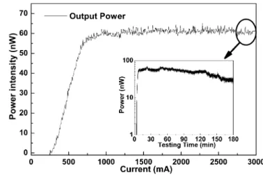
Fig. 7. Pulsed EL power as a function of the bias current. The inset figure is the lifetime and decaying rate of the Ag/SiO :Si/n-Si/Ag MOS diode under pulsed-current EL operation.
The turn-on voltage of the MOS diode under the pulsed driving condition is 5.8 V, which is much smaller than that of the Ag/SiO /n-Si/Al MOS diode reported previously [32]. The CW – measurements of the Ag/SiO Si /n-Si/Ag MOS diode further reveal a negative-differential-resistance effect with a threshold field strength (300 kV/cm) comparable to that of the GaN semiconductors (80-150 kV/cm) [33], [34]. The resistance of the Ag/SiO Si /n-Si/Ag MOS diode is about 7.9 at a bias voltage between 0–9 V, but the resistance decreases to 0.6 after turn-on. Significantly, the turn-on voltage of the Ag/SiO Si /n-Si/Ag MOS diode is almost one order of magnitude lower than that of an Ag/SiO /n-Si/Al diode (up to 50 V) reported by Yuan et al. [32]. Under pulsed current driving conditions, the optical power of the SiO Si MOS diode driven from 0 to 3 A is shown in Fig. 7. Extrapolating the output optical power as a function of the bias current or voltage reveals that the threshold current of the Ag/SiO Si /n-Si/Ag MOS light-emitting diode is 0.28 A. Such a low turn-on voltage of the emission of light from the Ag/SiO Si /n-Si/Ag MOS diode SiO Si sample with a SiO Si thickness of 500 nm is mainly attributed to the improvement (modification) of the carrier transport of the Ag/SiO Si /Si/Ag MOS diode, which is strongly related to the enhanced Fowler–Nordheim tun-neling behavior induced after the multi-energy Si-implantation process. The optical power increases by nearly four orders of magnitude as the drive current is increased from 0.28 to 0.97 A. The maximum optical power is about 120 nW at a bias current of 0.97 A. By measuring a single luminescent point of the Ag/SiO Si /n-Si/Ag diode with a lensed fiber, the power–cur-rent ( – ) slope is determined as to be 1.56 10 mW/A. Note that such a small slope is due to the measuring limit of the power sensor. The optical power at a constant drive current is relatively stable, with a fluctuation of less than 5%. As the drive current exceeds 1 A, the output power tends to saturate due to the finite density of minority carrier (holes) in n-Si injected into the SiO Si layer (see Fig. 7).
The EL wavelength of the Ag/SiO Si /n-Si/Ag MOS diode is completely different from that of an Ag/SiO /n-Si/Al diode (with red luminescence at wavelengths of 620-640 nm) [10]. In particular, the far-field EL patterns of the Ag/SiO Si /n-Si/Ag
(a) (b) (c)
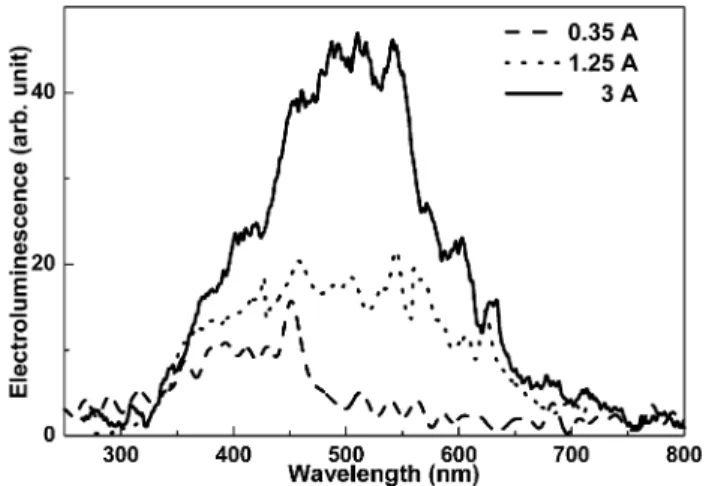
Fig. 8. Far-field EL patterns at different bias currents of (a) 0.35, (b) 1.25, and (c) 3 A.
Fig. 9. EL spectra of the Ag/SiO :Si /n-Si/Ag MOS diode at different bias currents of 0.35 (dashed line), 1.25 (dotted line), and 3 A (solid line).
MOS diode biased at various pulsed currents (see Fig. 8) re-veal different colors under different bias conditions. The deep-blue EL is more pronounced at a bias current near threshold, which turns into the white-light luminescence at a bias current of 1.25 A. However, the dominant EL wavelength further increases into the green region as the bias current becomes extremely high ( 2 A). At a bias current of 0.35 A, the deep-blue EL spec-trum (see Fig. 9) of the MOS diode is between 400–450 nm since the recombination by WOB defects is preferable under near-threshold conditions. The white-light EL spectrum of the MOS diode at a bias current of 1.25 A is between 400–600 nm, while the green EL spectrum at 3 A is between 450–550 nm. At a bias current of 1.25 A, the white-light emission is attributed to a full recombination through three different centers, including the WOB defects ( 415 nm), the NOV defects, and the de-fects ( 520 nm). At a high bias current ( 2 A), the green-region spectrum is clearly enhanced due to the highest density of NOV defects in SiO Si . The EL intensity at a bias current of 3 A is six times higher than that at 0.35 A. Additionally, the emission spot becomes larger at a higher bias. The lifetime testing of such an EL emitting diode is performed by measuring its time-de-pendent power characteristic, as shown in the inset of Fig. 7. Under a pulsed bias of 3 A, the decay in output power of the Ag/SiO Si /n-Si/Ag MOS diode under TEC cooling is up to 58% within 3 h.
E. Electroluminescent Mechanism of SiO Si
The EL spectrum of the Ag/SiO Si /n-Si/Ag MOS diode deviates slightly from that of the PL, which originates from an impact ionization and subsequent electron–hole recombination under a high electric field. Previously, Heikkilä et al. [35] have studied versatile carrier transport mechanisms of the
metal/SiO /p-Si/metal diode. The light emission from such a MOS diode is mainly dependent on the defects near the interface of the SiO /p-Si, which exhibits EL under both the forward and reverse bias conditions only when the contact metal is ohmic-like. The schematic energy-band diagrams of the metal/SiO /p-Si/metal structure under forward and reverse bias are shown in previous work [19], [32], [35]. If a forward bias is sufficiently large, most electrons from the negatively biased metal contact can tunnel through the SiO into the conduction band of p-Si substrate, and some electrons can be trapped by the higher energy levels of the defects in the SiO [19], [35]. The holes (majority carriers) in p-Si can also be injected into the SiO and be trapped by higher energy levels of the defects in the SiO . The radiative recombination of charged carriers at these occupied defect states in the SiO is responsible for the visible EL. When the metal/SiO /p-Si/metal diode is negatively biased, the holes can hardly be supported by the metal contact, and the electrons are the minority carriers in p-Si. Consequently, a strong EL is rather difficult unless the MOS diode is strongly reverse-biased.
In addition, Yuan et al. [32] also observed a visible EL at 620–640 nm from a reverse-biased Ag/native-SiO /n-Si/Al (referred to as Ag/SiO /n-Si/Al) diode, which results from the recombination of NBOHC centers near the SiO /n-Si interface. The carrier injection of such a diode structure relies on the field-dependent impact ionization [19], [32], [35]. Under a reverse bias, an inversion layer can be formed just beneath the SiO /n-Si interface, which accumulates the minority carriers (holes) in n-Si as shown in [32, Fig. 5(b)]. The tunneling electrons from the metal contact and holes from the n-Si are subsequently trapped and radiatively recombine through the NBOHC states. In particular, a forward bias fails to induce EL since it is difficult to inject holes from the positively biased metal contact. These observations correlate well with previous reports where the metal contact must supply electrons rather than holes. Such polarization dependence also excludes the possibility of EL from nc-Si (if it exists) within the SiO . Later on, Bae et al. [19] stated that the EL observed in an Au/SiO /p-Si/metal diode under reverse bias is attributed to the impact ionization of the ground-state electrons of the NOV centers in SiO . It is considered that luminescent efficiency by direct tunneling under a forward bias is less pronounced than that by impact ionization under reverse bias, although the direct tunneling helps the transport of carriers under forward bias conditions.
In comparison, our experimental results are somewhat similar to those reported previously [10], [22], which reveals that the EL of the Si-rich SiO Si layer decreases under forward-bias conditions [19], [36], [37]. The EL can only be obtained when the Ag–SiO Si /n-Si–Ag diode is reverse biased in our case, which is enhanced by stronger impact ionization on the ground states of defects via the accumulation of injected holes in the inversion layer formed beneath the SiO Si /n-Si interface. In general, multi-energy Si-ion implantation introduces high den-sities of various defects that are uniformly distributed in the thin SiO Si layer. With increasing bias, the tunneling electrons and holes can be trapped and subsequently recombine in the oc-cupied WOB defect, NOV defects, and defects. A higher electric field increases the band bending in the accumulation
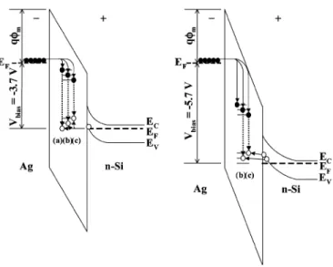
Fig. 10. Energy-band diagrams of the Ag/SiO :Si /n-Si/Ag structure with metal–oxide barrier potential of = 3.28 V under reverse bias at 3.7 V (left) and 5.7 V (right). Three defect-related radiative emissions at (a) 415 nm from the WOB defect, (b) 455 nm from the NOV defect, and (c) 520 nm from theE defect.
layer, which facilitates the tunneling of holes from the n-Si sub-strate to the ground states of NOV and defects (see Fig. 10). Such an operation greatly enhances the transitions contributing to the blue–yellow luminescence. Both of the transitions con-tributed by the WOB defects and NOV defects can emit the deep-blue luminescence at lower bias currents. The white-light EL emission is observed when the bias current increases be-fore the saturation of output power. The green EL from the will be enhanced when the bias current (as well as the elec-tric field) becomes extremely high. The reason for the saturated output power at a bias current of nearly 1 A is due to the lim-ited density of the minority carriers (holes) in the n-Si substrate. A stronger bias seriously bends the inversion layer beneath the SiO Si /n-Si interface and thus greatly accumulates the holes at lower states, which subsequently tunnel into the defects at higher energy levels (see Fig. 10). This effect results in longer luminescent wavelengths at higher bias conditions. Nonethe-less, such an impact ionization process usually requires a strong bias, which inevitably causes the substrate to overheat.
IV. CONCLUSION
The white-light and blue–green EL from an Ag/SiO Si /n-Si/Ag MOS diode with the defect-en-hanced blue–green PL, made on a thermally annealed multirecipe Si-ion-implanted SiO Si film on an Si substrate with a nearly depth-independent Si-dose distribution profile, are studied. After annealing for 180 min, the main radiative defects corresponding to PL at 415, 455, and 520 nm are completely activated. These defects are identified as WOB, the NOV-related defects, and -related defects, respectively. Ion implantation introduces more dangling bond defects than other methods (such as PECVD and sputtering) for synthesizing the Si-rich SiO . During the Si implantation (or physical bombardment with high-energy ions), the oxygen vacancies and the oxygen interstitials (the precursors for the WOB defects) are created due to the relatively large quantities of
structures have not yet been well constructed. The EL power of the Ag/SiO Si /n-Si/Ag MOS diode increases linearly with bias current after turn-on and saturates near 0.97 A. The EL of the Ag/SiO Si /n-Si/Ag MOS diode turns from blue to white-light emission when the bias current is close to the saturation condition and eventually changes to a yellow–green emission as the bias current is increased to 3 A. The EL spectrum of the MOS diode under different reverse-bias conditions indicates that the radiative recombination is due to enhanced impact ionization of ground states of defects, such as WOB, NOV, and defects, through the injection of holes accumulated in the inversion layer formed beneath the SiO Si /n-Si interface.
ACKNOWLEDGMENT
The authors would like to thank Dr. J.-M. Shieh, National Nano Device Laboratory, for his technical support.
REFERENCES
[1] Q. Ye, R. Tsu, and E. H. Nicollian, “Resonant tunneling via microcrys-talline-silicon quantum confinement,” Phys. Rev. B, Condens. Matter, vol. 44, no. 4, pp. 1806–1811, July 1991.
[2] A. Pèrez-Rodrìguez, O. González-Varona, B. Garrido, P. Pellegrino, J. R. Morante, C. Bonafos, M. Carrada, and A. Claverie, “White lumines-cence from Si and C ion-implanted SiO films,” J. Appl. Phys., vol. 94, no. 1, pp. 254–261, Jul. 2003.
[3] D. Pacifici, E. C. Moreira, G. Franzo, V. Martorino, and F. Priolo, “De-fect production and annealing in ion-irradiated Si nanocrystals,” Phys.
Rev. B, Condens. Matter, vol. 65, no. 14, pp. 144 109-1–144 109-13, Apr.
2002.
[4] L. T. Canham, “Silicon quantum wire array fabrication by electrochem-ical and chemelectrochem-ical dissolution of wafers,” Appl. Phys. Lett., vol. 57, no. 10, pp. 1046–1048, Sep. 1990.
[5] X. Zhao, O. Schoenfeld, J. Kusano, Y. Aoyagi, and T. Sugano, “Observa-tion of direct transi“Observa-tions in silicon nanocrystallites,” Jpn. J. Appl. Phys., vol. 33, no. 7A, pp. L899–L901, Jul. 1994.
[6] P. Mutti, G. Ghislotti, S. Bertoni, L. Bonoldi, G. F. Cerofolini, L. Meda, E. Grilli, and M. Guzzi, “Room-temperature visible luminescence from silicon nanocrystals in silicon implanted SiO layers,” Appl. Phys. Lett., vol. 66, no. 7, pp. 851–853, Feb. 1995.
[7] T. Shimizu-Iwayama, K. Fujita, S. Nakao, K. Saitoh, T. Fujita, and N. Itoh, “Visible photoluminescence in Si -implanted silica glass,” J.
Appl. Phys., vol. 75, no. 12, pp. 7779–7783, Jun. 1994.
[8] H. Takagi, H. Owada, Y. Yamazaki, A. Ishizaki, and T. Nakagiri, “Quantum size effects on photoluminescence in ultrafine Si particles,”
Appl. Phys. Lett., vol. 56, no. 24, pp. 2379–2380, Jun. 1990.
[9] S. Tong, X. N. Liu, T. Gao, and X. M. Bao, “Intense violet-blue photolu-minescence in as-deposited amorphous Si:H:O films,” Appl. Phys. Lett., vol. 71, no. 5, pp. 698–700, Aug. 1997.
[10] L. S. Liao, X. M. Bao, X. Q. Zheng, N. S. Li, and N. B. Min, “Blue luminescence from Si -implanted SiO films thermally grown on crys-talline silicon,” Appl. Phys. Lett., vol. 68, no. 6, pp. 850–852, Feb. 1996.
[11] H. Z. Song, X. M. Bao, N. S. Li, and J. Y. Zhang, “Relation between electroluminescence and photoluminescence of Si -implanted SiO ,”
J. Appl. Phys., vol. 82, no. 8, pp. 4028–4032, Oct. 1997.
[12] G. G. Qin, A. P. Li, B. R. Zhang, and B. C. Li, “Visible electrolumi-nescence from semitransparent au film/extra thin Si-rich silicon oxide film/p-Si structure,” J. Appl. Phys., vol. 78, no. 3, pp. 2006–2009, Aug. 1995.
[13] H. Z. Song and X. M. Bao, “Visible photoluminescence from silicon-ion-implanted SiO film and its multiple mechanisms,” Phys. Rev. B,
Condens. Matter, vol. 55, no. 11, pp. 6988–6993, Mar. 1997.
[14] W. Hayes, M. J. Kane, O. Salminen, R. L. Wood, and S. P. Doherty, “ODMR of recombination centers in crystalline quartz,” J. Phys. C:
Solid State Phys., vol. 17, pp. 2943–2951, Dec. 1984.
[15] H. Nishikawa, E. Watanabe, D. Ito, M. Takiyama, A. Leki, and Y. Ohki, “Photoluminescence study of defects in ion-implanted thermal SiO films,” J. Appl. Phys., vol. 78, no. 2, pp. 842–846, Jul. 1995.
[16] R. Tohmon, Y. Shimogaichi, H. Mizuno, Y. Ohki, K. Nagasawa, and Y. Hama, “2.7-eV luminescence in as-manufactured high-purity silica glass,” Phys. Rev. Lett., vol. 62, no. 2, pp. 1388–1391, Mar. 1989. [17] H. Nishikawa, R. E. Stahlbush, and J. H. Stathis,
“Oxygen-defi-cient centers and excess Si in buried oxide using photoluminescence spectroscopy,” Phys. Rev. B, Condens. Matter, vol. 60, no. 23, pp. 15 910–15 918, Dec. 1999.
[18] J. C. Cheang-Wong, A. Oliver, J. Roiz, J. M. Hernandez, L. Ro-drigues-Fernandez, J. G. Morales, and A. Crespo-Sosa, “Optical properties of Ir -implanted silica glass,” Nucl. Instr. Meth. B, vol. 175–177, pp. 490–494, Apr. 2001.
[19] H. S. Bae, T. G. Kim, C. N. Whang, S. Im, J. S. Yun, and J. H. Song, “Electroluminescence mechanism in SiO layers containing radiative centers,” J. Appl. Phys., vol. 91, no. 7, pp. 4078–4081, Apr. 2002. [20] E. H. Poindexter and P. J. Caplan, “Electron spin resonance of inherent
and process induced defects near the Si/SiO interface of oxidized sil-icon wafers,” J. Vac. Sci. Technol. A, vol. 6, no. 3, pp. 1352–1357, May 1988.
[21] B. L. Zhang and K. Raghavachari, “Photoabsorption and photolumines-cence of divalent defects in silicate and germanosilicate glasses: First-principles calculations,” Phys. Rev. B, Condens. Matter, vol. 55, no. 24, pp. R15993–R15996, June 1997.
[22] K. Vanheusden and A. Stesmans, “Characterization and depth profiling ofE defects in buried SiO ,” J. Appl. Phys., vol. 74, no. 1, pp. 275–283, Jul. 1993.
[23] Y. Sakurai and K. Nagasawa, “Green photoluminescence band in -ir-radiated oxygen-surplus silica glass,” J. Appl. Phys., vol. 86, no. 3, pp. 1377–1381, Aug. 1999.
[24] H. Nishikawa, E. Watanabe, D. Ito, Y. Sakurai, K. Nagasawa, and Y. Ohki, “Visible photoluminescence from Si clusters in -irradiated amor-phous SiO ,” J. Appl. Phys., vol. 80, no. 6, pp. 3513–3517, Sep. 1996. [25] M. Y. Valakh, V. A. Yukhimchuk, V. Y. Bratus, A. A. Konchits, P. L.
F. Hemment, and T. Komoda, “Optical and electron paramagnetic reso-nance study of light-emitting Si ion implanted silicon dioxide layers,”
J. Appl. Phys., vol. 85, no. 1, pp. 168–173, Jan. 1999.
[26] B. L. Zhang and K. Raghavachari, “Photoabsorption and photolumines-cence of divalent defects in silicate and germanosilicate glasses: First-principles calculations,” Phys. Rev. B, Condens. Matter, vol. 55, no. 24, pp. R15993–R15996, June 1997.
[27] C. Barthou, P. H. Duong, A. Oliver, J. C. Cheang-Wong, L. Rodríguez-Fernández, A. Crespo-Sosa, T. Itoh, and P. Lavallard, “Silicon nanocrys-tals and defects produced by silicon and silicon-and-gold implantation in silica,” J. Appl. Phys., vol. 93, no. 12, pp. 10 110–10 113, Jun. 2003. [28] A. Anedda, R. Boscaino, M. Cannas, R. Corpino, F. M. Gelardi, and M.
Leone, “Experimental evidence of the composite nature of the 3.1 eV luminescence in natural silica,” Nucl. Instrum. Methods Phys. Res. B, vol. 116, no. 1–4, pp. 360–363, Aug. 1996.
[29] R. A. Weeks and E. Sonder, Paramagnetic Resonance. New York: Academic, 1963, pp. 869–869.
[30] L. Skuja, “Direct singlet-to-triplet optical absorption and luminescence excitation band of the twofold-coordinated silicon center in oxygen-de-ficient glassy SiO ,” J. Non-Cryst. Solids, vol. 167, no. 3, pp. 229–238, Feb. 1994.
[31] , “Optically active oxygen-deficiency-related centers in amorphous silicon dioxide,” J. Non-Cryst. Solids, vol. 239, no. 1–3, pp. 16–48, Oct. 1998.
[32] J. Yuan and D. Haneman, “Visible electroluminescence from native SiO on n-type Si substrates,” J. Appl. Phys., vol. 86, no. 4, pp. 2358–2360, Aug. 1999.
[33] G.-R. Lin, “The structural and electrical characteristics of silicon-im-planted borosilicate glass,” Jpn. J. Appl. Phys., vol. 41, no. 12A, pp. L1379–L1382, Dec. 2002.
[34] E. Alekseer and D. Pavlidis, “Large-signal microwave performance of GaN-based NDR diode oscillators,” Solid-State Electron., vol. 44, no. 6, pp. 941–947, Jun. 2000.
[35] L. Heikkilä, T. Kuusela, and H.-P. Hedman, “Electroluminescence in Si/SiO layer structures,” J. Appl. Phys., vol. 89, no. 4, pp. 2179–2184, Feb. 2001.
[36] M. Kimura and H. Koyama, “Mechanism of time-dependent oxide breakdown in thin thermally grown SiO films,” J. Appl. Phys., vol. 85, no. 11, pp. 7671–7681, Jun. 1999.
[37] H. J. Wen and R. Ludeke, “Investigation of existing defects and defect generation in device-grade SiO by ballistic electron emission spec-troscopy,” J. Vac. Sci. Technol. B, vol. 15, no. 4, pp. 1080–1088, Jul. 1997.
Chun-Jung Lin was born in Taipei, Taiwan, R.O.C., in 1973. He received the B.S. degree in electrical engineering from Feng Chia University, Taichung, Taiwan, in 1998 and the M.S. degree in electrooptic engineering from Tatung University, Taipei, in 2000. He is currently working toward the Ph.D. degree in electrooptic engineering at the National Chiao Tung University, Hsinchu, Taiwan.
From 2001 to 2002, he was with Kingfont Inc., Taipei, as a Senior Engineer, where he was involved with fiber transceivers. His research interests are in the design, fabrication, and analysis of nanocrystal photonic components for light-emitting devices.
Gong-Ru Lin (S’92–M’97–SM’04) received the M.S. and Ph.D. degrees from National Chiao Tung University (NCTU), Hsinchu, Taiwan, R.O.C., in 1990 and 1996, respectively.
He joined NCTU as an Associate Professor with the Institute of Electro-Optical Engineering in 2002. His research interests are in ultrafast fiber lasers and optoelectronics, microwave and millimeter-wave photonics, and amorphous or nanocrystallite semi-conductors. He has (co)authored more than 70 papers in international periodicals and over 100 papers in international conferences.
Dr. Lin is currently a Senior Member of the IEEE Lasers and Electro-Optics and Microwave Theory and Techniques Societies and a member of the Optical Society of America and SPIE. He has been included in Who’s Who in Science
and Engineering, (6th ed.) since 2002. He was the recipient of the Tien Jea
Bien Young Scholar Prize by the Optical Engineering Society of the Republic of China for his outstanding achievement in photonics.