The Annihilation of Threading Dislocations in the Germanium
Epitaxially Grown within the Silicon Nanoscale Trenches
Guang-Li Luo,a,zShih-Chiang Huang,aChih-Hsin Ko,bClement H. Wann,b
Cheng-Ting Chung,c Zong-You Han,c Chao-Ching Cheng,c Chun-Yen Chang,c
Hau-Yu Lin,band Chao-Hsin Chiena,c a
National Nano Device Laboratories, Hsinchu 300, Taiwan b
Taiwan Semiconductor Manufacturing Company, Limited, Hsinchu 300, Taiwan c
Institute of Electronics, National Chiao-Tung University, Hsinchu 300, Taiwan
We investigated the selective growth of germanium into nanoscale trenches on silicon substrates. These nanoscale trenches, the smallest size of which was 50 nm, were fabricated using the state-of-the-art shallow trench isolation technique. The quality of the Ge films was evaluated using transmission electron microscopy. The formation of threading dislocations共TDs兲 was effectively suppressed when using this deposition technique. For the Ge grown in nanoscale Si areas共e.g., several tens of nanometers兲, the TDs were probably readily removed during cyclic thermal annealing predominantly because their gliding distance to the SiO2
sidewalls was very short. Therefore, nanoscale epitaxial growth technology can be used to deposit Ge films on lattice-mismatched Si substrates with a reduced defect density.
© 2009 The Electrochemical Society. 关DOI: 10.1149/1.3158832兴 All rights reserved.
Manuscript submitted March 10, 2009; revised manuscript received June 3, 2009. Published July 6, 2009.
Because of the higher mobility of its carriers and its narrower bandgap relative to that of silicon 共Si兲,1 germanium 共Ge兲 is now emerging as a viable candidate to supplement Si in complementary metal oxide semiconductor共CMOS兲 devices and 1.3–1.55 m op-toelectronic applications;2 therefore, it is essential to develop new methods for the heteroepitaxial growth of Ge on Si. This growth process is not straightforward, however, because the large lattice mismatch共4%兲 between Ge and Si limits the quality of the epitaxi-ally grown layers. After reaching a critical thickness, the Ge layer usually contains many misfit dislocations共MDs兲 and threading dis-locations共TDs兲, making it unusable for any practical applications. Although several techniques have been proposed to alleviate this problem,3the TD densities in the grown Ge layers remain too high for device applications. Using patterned growth and cyclic thermal annealing共CTA兲, the dislocation density in Ge can be reduced to ca. 106/cm2 as a result of thermally induced dislocation gliding.4Any further reduction remains a big challenge because the dislocations cannot glide over the long distances in large patterns. Based on the selective growth of Ge in narrow, deep SiO2 trenches of several hundreds of nanometers, it was recently reported that the generated TDs in Ge could be effectively trapped to the sidewalls of SiO2 through an aspect ratio trapping共ART兲 mechanism;5 the resulting top area of Ge was claimed to be dislocation free. In Ref. 5, the authors considered that the TDs formed at a 45° angle to the under-lying Si共001兲 surface. Thus, for trenches having an aspect ratio greater than unity, the TDs meet the SiO2sidewalls and terminate there when they penetrate up in the Ge film. In such a case, the surface of Ge would be dislocation free, with TDs being confined only to the bottom of the trenches.
In this study, following the similar process scheme, we selec-tively grew Ge layers in SiO2trenches having dimensions as low as
50 nm. After CTA, the formation of TDs in the Ge layers grown in these ultrasmall trenches was further suppressed. Our results are slightly different from those expected for the ART mechanism,5 where there are still a few TDs at the bottom of the Ge layer. In our case, the dislocations at the bottom of the trenches were also sup-pressed, quite advantageous for the fabrication of Si-based Ge-channel devices, such as Ge fin field effect transistor共FinFET兲 de-vices. For our Ge films grown in ultrasmall SiO2trenches, the TD
reduction was readily achieved because the TDs did not have to glide very long distances in the nanoscale patterns.
Experimental
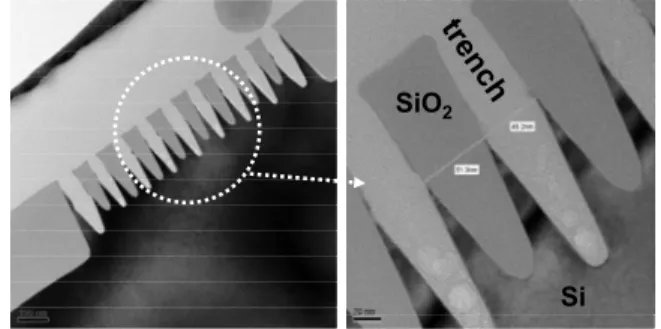
The state-of-the-art shallow trench isolation共STI兲 technique was used to fabricate the patterns on p-type 共100兲-oriented Si wafers having resistivities of 15–25 ⍀ cm. The Si area was recessed using reactive ion etching to form trenches for the selective epitaxial growth of Ge. The trenches were aligned along the关110兴 direction; they were formed with dimensions of 50 nm⫻ 600 nm and 320 nm⫻ 1.4 m, respectively. The narrowest width of the trenches was 50 nm, a reasonable dimension for 22 nm technology nodes. The finished 50 nm trenches are displayed in Fig.1. After trench fabrication, the Si substrates were subjected to standard wet cleaning and dipping in dilute HF for 30 s to remove the native oxide on the exposed Si surface; they were then loaded into an ultrahigh vacuum chemical vapor deposition chamber. After thermal prebaking at 900°C for 10 min, Ge layers having thicknesses of 150–200 nm were selectively grown inside the trenches at 400°C under a germane flow rate of 10 sccm and a growth pressure of 0.5 mTorr. Finally, the wafers were in situ annealed over three cycles; each cycle included high temperature annealing at 900°C for 5 min and low temperature annealing at 400°C for 5 min. Because the thermal expansion coefficients of Ge and Si are different, annealing can generate extra thermal stress that can cause movement of the TDs in the grown Ge layer. For CTA, an increase in the number of cycles results in a greater dislocation reduction.4,6In this study, con-sidering the trade-off between the thermal stress effect and the ex-perimental efficiency, a three-cycle annealing was adopted. Cross-sectional transmission electron microscopy共XTEM兲 and plan-view transmission electron microscopy 共TEM兲 samples were prepared through mechanical polishing and perforation by Ar-ion milling. For the plan-view TEM samples, only the top 70 nm Ge layer remained
z E-mail: [email protected] Si SiO2
tre
nc
h
Si SiO2 Si SiO2tre
nc
h
Figure 1. XTEM images of the 50 nm SiO2trenches fabricated using the
STI process.
Journal of The Electrochemical Society, 156共9兲 H703-H706 共2009兲
0013-4651/2009/156共9兲/H703/4/$25.00 © The Electrochemical Society H703
) unless CC License in place (see abstract).
ecsdl.org/site/terms_use
address. Redistribution subject to ECS terms of use (see
140.113.38.11
after Ar-ion milling, making sure that the Ge/Si interface region was removed. TEM images were recorded using an FEI Tecnai F20 mi-croscope operated at 200 kV.
Results and Discussion
TDs are associated with MDs at an interface; they are necessary to accommodate the lattice mismatch between Ge and Si. The MDs can terminate at the film surface via TDs. For diamond and zinc-blende semiconductors, there are generally two types of MDs at the interface: 60° dislocations, which are glissile and have a Burgers vector b out of the interface plane, and 90° dislocations, which are sessile and have b lying in the interface plane. The 60° MDs can change their length during plastic relaxation through the gliding of their threading segment. The 90° MDs are very effective in relieving a lattice mismatch, but their threading segments can hardly glide.7,8 For face-centered cubic semiconductors, gliding on the close-packed 兵111其 glide planes of a 60° dislocation is preferable to that on the 兵100其 glide planes of a 90° dislocation; therefore, a direct formation of 90° dislocations is difficult.7 This type of dislocation can be formed, however, through the reaction of two 60° dislocations.9,10 For example, if two 60° dislocations had Burgers vectors such that a strong attraction existed between the two threading segments 共b1
and b2兲, an attractive interaction would generate a TD having a
Burgers vector b3, namely, a 90° dislocation. In terms of Burgers vectors, a typical reaction may be written as
共a/2兲关011¯兴 + 共a/2兲关101兴 = 共a/2兲关110兴
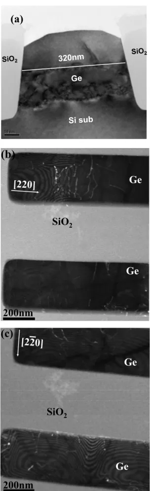
Figure2adisplays an XTEM image of the Ge film in a trench having a width of 320 nm; it reveals that the TDs could not be removed completely through CTA. Figure2b and c presents two-beam dark-field plan-view TEM images that were recorded on the same area of the sample by using g =关220兴 and 关22¯0兴 reflections, respectively; TDs also appear in these two images. The dislocations that display a clear contrast in Fig.2bare invisible in Fig.2c, and vice versa. The Burgers vector of these dislocations can be easily identified by the invisibility criterion because dislocations lose con-trast if g is perpendicular to the Burgers vector共i.e., g · b = 0兲.11 Based on this criterion, the dislocations in Fig.2bandcare all 90°. The 90° dislocations in Fig. 2b must have a Burgers vector of a/2关110兴 because they are invisible in Fig.2c; in contrast, the 90° dislocations in Fig.2cmust have a Burgers vector of a/2关11¯0兴 be-cause they are invisible in Fig.2b. We observe no 60° dislocations in these two figures; therefore, they must have been removed during CTA through the glide and annihilation mechanisms.12 The Ge/Si interface was somewhat undulated. The high temperature CTA pro-cess was the likely cause of this roughness because high temperature annealing can result in severe interdiffusion of Ge and Si. The high gliding ability of the 60° dislocations in the grown Ge layer can be understood in terms of their velocity. We estimated the maximum in-plane thermal stress caused by CTA treatment in our case to be on the order of 109 dyn/cm2. The glide velocity of the 60° dislocations
is on the order of 10−3 cm/s, according to the data in Kabler’s early
report.13
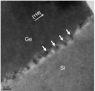
Figure 3 presents XTEM and plan-view TEM images of Ge grown in 50 nm trenches. In Fig.3ato c , no TDs are evident in Ge, even at its bottom; only MDs appear at the interface of Ge/Si共see Fig.3bandd兲. From these results, we conclude that the TDs glided
out the Ge during CTA, and only MDs remained along the Ge/Si interface. A comparison of Fig.1and3reveals that the Si along the SiO2sidewalls at the bottom areas of trenches disappeared after the Ge growth presumably because intense interdiffusion occurred be-tween Si and Ge during the CTA process. That is, Si on both sides of each trench completely diffused into the Ge film during annealing. For comparison, we observed TDs when the Ge layers grown inside the 50 nm trenches were not subjected to CTA共see Fig.4兲,
confirm-ing that CTA was essential for the removal of TDs.
According to Speck et al.10and Romanov et al.,14the TD densi-ties can be reduced either through the annihilation of threading
seg-SiO
2200nm
Ge
Ge
[220]
SiO
2200nm
Ge
Ge
[220]
(b)
SiO
2200nm
Ge
Ge
[220]
SiO
2200nm
Ge
Ge
[220]
SiO
2200nm
Ge
Ge
[220]
(c)
320nm
SiO2 SiO2Si sub
Ge
320nm
SiO2 SiO2Si sub
Ge
(a)
320nm
SiO2 SiO2Si sub
Ge
320nm
SiO2 SiO2Si sub
Ge
(a)
Figure 2. 共a兲 XTEM image of Ge in trenches having a width of 320 nm,
revealing unremoved dislocations. Plan-view TEM images of Ge in trenches having a width of 320 nm:共b兲 g = 关220兴; 共c兲 g = 关22¯0兴.
H704 Journal of The Electrochemical Society, 156共9兲 H703-H706 共2009兲 H704
) unless CC License in place (see abstract).
ecsdl.org/site/terms_use
address. Redistribution subject to ECS terms of use (see
140.113.38.11
ments having antiparallel Burgers vectors or through reactions in which two TDs combine to form one TD. There are four possible annihilation processes for TDs in a dislocated epitaxial film: 共i兲 Loops can self-annihilate through gliding; 共ii兲 threading segments from different sources on the same slip lane can annihilate or com-bine to form another one through gliding;共iii兲 threading segments from different sources on the parallel slip systems can annihilate or combine to form another one;共iv兲 threading segments from different sources on intersecting slip systems can annihilate or combine to form another one through gliding, climbing, or a combination of the two. Because Ge and Si have a 4% lattice mismatch, the original TD density should be the same for any pattern size. Here, the major factor determining the TD density should be the propagation dis-tance. In the nanoscale patterns, many of the dislocations could readily glide to the sidewalls of the trenches with a low probability
of being blocked or combined to form a sessile dislocation because of the very small propagation length; in contrast, dislocations in larger patterns had greater difficulty arriving at the sidewalls, and, therefore, they tended to become trapped in the Ge film. Although the trench was aligned along the关110兴 direction and had a length of 600 nm, the TD density still remained low. Because the TDs in the 共1¯1¯1兲 and 共111兲 slip planes along the width direction of the trench 共i.e., 关110兴 direction兲 have glided to the SiO2sidewalls, the
interac-tions between TDs from different sources on intersecting slip sys-tems 关e.g., between 共1¯1¯1兲 and 共11¯1兲 slip planes兴 are suppressed. This case facilitates the annihilation of TDs on the same slip plane or on the parallel slip systems 关e.g., the 共ii兲 and 共iii兲 annihilation processes of TDs described above兴 to work better along the direction of the length of the trench. As a result, the TD density in 50 nm trenches can still be reduced, albeit the length of the trenches is long.
Recent publications15 suggest that for SiGe films grown selec-tively on recessed Si, a decrease in the trench width causes the strain of the SiGe film to be released preferably through elastic relaxation in the direction of the width of the trench. However, the strain in our Ge film was released mainly through plastic relaxation in the direc-tions of both the width and the length. In Fig.3bandd, uniformly distributed MDs appear at the Ge/Si interface. For comparison, we also present a magnified XTEM image of the 50 nm sample along the direction of the length of the trenches. Similarly, the MDs are clearly observable at the Ge–Si interface in Fig.5. The distances between the MDs in Fig.3banddare almost the same as that in Fig.
5, indicating that the strain in Ge was relaxed biaxially and plasti-cally. This result differs from that reported by Ref.15 most likely because we applied a high temperature CTA process to the Ge layer, causing the Ge layer to relax adequately.
Conclusions
We have performed the heteroepitaxial growth of Ge into nano-scale trenches on Si substrates. Through mechanisms involving glid-ing and annihilation, the TDs in nanoscale Ge were readily removed through CTA. The strain in the Ge films grown using this technique was released mainly through plastic relaxation in the directions of both the width and the length of the trenches. This heterostructural Ge on Si probably has potential applications in the integration of Ge-channel devices onto Si CMOS platforms.
Si SiO2 SiO2 50nm 40nm Si SiO2 20nm Ge fin Si SiO2 20nm Ge fin Si SiO2 20nm Ge fin Si SiO2 20nm Ge fin
(a)
(b)
Ge SiO2 50nm SiO2 Ge SiO2 50nm SiO2(c)
Si Ge 10nm(d)
Si SiO2 SiO2 50nm 40nm Si SiO2 20nm Ge fin Si SiO2 20nm Ge fin Si SiO2 20nm Ge fin Si SiO2 20nm Ge fin(a)
(b)
Ge SiO2 50nm SiO2 Ge SiO2 50nm SiO2(c)
Si Ge 10nm(d)
Si SiO2 SiO2 50nm 40nm Si SiO2 20nm Ge fin Si SiO2 20nm Ge fin Si SiO2 20nm Ge fin Si SiO2 20nm Ge fin(a)
(b)
Ge SiO2 50nm SiO2 Ge SiO2 50nm SiO2(c)
Si Ge 10nm(d)
Figure 3.共a兲 XTEM image of Ge in trenches having a width of 50 nm. 共b兲
Magnified XTEM image.共c兲 Plan-view TEM image. 共d兲 Magnified XTEM image. The MDs at the Ge/Si interface are indicated by arrows.
dislocations
dislocations
Figure 4. XTEM image of Ge in 50 nm trenches without CTA.
[110]
Ge
Si
[110]Ge
Si
[110]Ge
Si
[110]Ge
Si
Figure 5. XTEM image of Ge in 50 nm trenches, recorded along the
direc-tion of the length of the trenches. MDs are clearly evident at the Ge/Si interface共some are indicated by arrows兲.
H705 Journal of The Electrochemical Society, 156共9兲 H703-H706 共2009兲 H705
) unless CC License in place (see abstract).
ecsdl.org/site/terms_use
address. Redistribution subject to ECS terms of use (see
140.113.38.11
National Nano Device Laboratories assisted in meeting the publication costs of this article.
References
1. H. Shang, K. L. Lee, P. Kozlowski, C. D’Emic, I. Babich, E. Sikorski, M. Ieong, H. S. P. Wong, K. Guarini, and W. Haensch, IEEE Electron Device Lett., 25, 135 共2004兲.
2. Z. H. Huang, J. Oh, S. K. Banerjee, and J. C. Campbell, IEEE J. Quantum
Elec-tron., 43, 238共2007兲.
3. T. Myrberg, A. P. Jacob, O. Nur, M. Friesel, M. Willander, C. J. Patel, Y. Cam-pidelli, C. Hernandez, O. Kermarrec, and D. Bensahel, J. Mater. Sci.: Mater.
Elec-tron., 15, 411共2004兲, and references therein.
4. H.-C. Luan, D. R. Lim, K. K. Lee, K. M. Chen, J. G. Sandland, K. Wada, and L. C. Kimerling, Appl. Phys. Lett., 75, 2909共1999兲.
5. J. S. Park, J. Bai, M. Curtin, B. Adekore, M. Carroll, and A. Lochtefeld, Appl.
Phys. Lett., 90, 052113共2007兲.
6. M. Yamaguchi and S. Kondo, Mater. Res. Soc. Symp. Proc., 45, 279共1989兲. 7. D. Hull and D. J. Bacon, Introduction to Dislocations, 4th ed., pp. 82–98,
Butterworth-Heinemann, Woburn, MA.共2001兲.
8. J. W. Matthews and A. E. Blakeslee, J. Cryst. Growth, 32, 265共1976兲. 9. R. Beanland, D. J. Dunstan, and P. J. Goodhew, Adv. Phys., 45, 87共1996兲. 10. J. S. Speck, M. A. Brewer, G. Beltz, A. E. Romanov, and W. Pompe, J. Appl.
Phys., 80, 3808共1996兲.
11. P. B. Hirsh, A. Howie, R. B. Nicholson, D. W. Pashley, and M. J. Whealan,
Electron Microscopy of Thin Crystals, p. 176, Butterworths, London共1965兲.
12. G. E. Beltz, M. Chang, M. A. Eardley, W. Pompe, A. E. Romanov, and J. S. Speck,
Mater. Sci. Eng., A, 234–236, 794共1997兲. 13. M. N. Kabler, Phys. Rev., 131, 54共1963兲.
14. A. E. Romanov, W. Pompe, S. Mathis, G. E. Beltz, and J. S. Speck, J. Appl. Phys.,
85, 182共1999兲.
15. J. P. Liu, J. Li, A. See, M. S. Zhou, and L. C. Hsia, Appl. Phys. Lett., 90, 261915 共2007兲.
H706 Journal of The Electrochemical Society, 156共9兲 H703-H706 共2009兲 H706
) unless CC License in place (see abstract).
ecsdl.org/site/terms_use
address. Redistribution subject to ECS terms of use (see
140.113.38.11