Optimization on configuration of surface conduction electron-emitters
Hui-Wen Cheng
a, Yiming Li
a,b,*a
Department of Electrical Engineering and Institute of Communications Engineering, National Chiao Tung University, 1001 Ta-Hsueh Road, Hsinchu 300, Taiwan
b
National Nano Device Laboratories, Hsinchu 300, Taiwan
a r t i c l e
i n f o
Article history:
Received 29 November 2009
Received in revised form 8 January 2010 Available online 23 March 2010
a b s t r a c t
In this work, a novel nanogap with inclined protrusion cathode in palladium strip fabricated by hydrogen absorption under high-pressure treatment is optimized for the surface conduction electron-emitter. Its field emission is sensitive to the geometry of surface conduction electron-emitters (SCE). For a specified emitter material, the SCE are further investigated by varying the thickness, tilted angle and gap of palla-dium (Pd). An optimal field emission efficiency with 80° tilted angle, 120 nm gap and 10 nm thickness of Pd is found for certain designed field emission efficiency. We further find that varying the emitter mate-rial work function of the emitter matemate-rial from 5.12 eV to 3.9 eV will further improve the field emission property due to the increase of the emitted current.
Ó 2010 Elsevier Ltd. All rights reserved.
1. Introduction
Electrodes with nanometer separation have lots of different applications, such as molecular electronics [1,2] and vacuum microelectronics[3]. One of emerging technologies of nanogap is the surface conduction electron-emitter (SCE)[4]for the flat panel displays (FPDs) applications which has attracted much attention since reported by Sakai et al.[5]. The SCE display (SED) is an ad-vanced type of FPD based upon SCEs. The critical process step to fabricate SCEs is to create a nanofissure on a line electrode for the electron emission. SEDs have some attractive advantages, such as high-quality image, high resolution, quick response time, as well as low power consumption[6]. However, the nanogap fabrication process is such complicated and expensive. We notice that the field emission (FE) efficiency and current density of these FE cathodes further depend on both their geometry and fabrication materials. For the SCE, emission is obtained with a large electric field by a driving voltage that causes electrons to tunnel over a potential bar-rier out of the emitter to the driving electrode and anode. The emit-ter’s geometry increases emission by enhancing the electric field and reducing the barrier over which the electrons must tunnel.
In this work, we theoretically optimized the fabricated a palla-dium (Pd) nanogap electrode with a well-defined gap size[7,8]. For a fixed emitter material work function, the SCEs are investigated by varying the thickness, the tilted angle and the gap of palladium (Pd). Optimal field emission efficiency with 80° tilted angle,
120 nm gap and 10 nm thickness of Pd could be found. We have found that the proposed SCE with a smaller emitter material work function for the emitter material will induce a larger emitted cur-rent, which may increase the collected current on the anode. It pos-sesses higher field emission with higher focusing capability, compared with proposed SCE with a larger work function of Pd in the part of cathode, as shown inFig. 1.
2. Structure and simulation
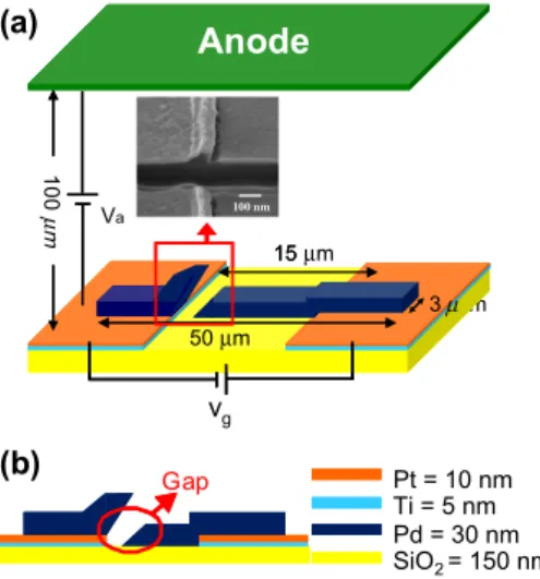
Fig. 1a schematically shows the structure of FPD based upon SCEs. Firstly, the substrate is formed by a p-type (100) silicon (Si) wafer. On silicon substrate, a 150-nm-thick SiO2layer was
ther-mally grown. An adhesion layer which was made by titanium (Ti) with 5-nm-thick is deposited by electron-beam-evaporation (e-beam) on the oxide. On the top of titanium, the Platinum (Pt) with a 10 nm thickness thin film is as well as deposited by e-beam. By a lift-off process, the pattern of Pt/Ti line electrodes with 80
l
m width was photolithographically performed. On the Pt/Ti bottom electrode, the Pd with 30 nm thickness thin film[9,10]was depos-ited by e-beam. And the lift-off method was also used to pattern the Pd electrode line of 50l
m length and 3-l
m width[11–13]. Un-der high-pressure treatment, a nanogap with a separation on the Pd strip was then produced by hydrogen absorption. About the an-ode, we use screen printing to obtain phosphor thick films. Then the aluminium coating with the thickness of 50–300 nm was evap-orated on some phosphor films. A clear description of fabrication and characterization could be found in our previous work[14,15]. For investigating the field emission properties in SCE, the FDTD-PIC[16–19]codes are implemented. Starting from a specified ini-tial state, we simulate electrostatic fields as its evolution in time.0026-2714/$ - see front matter Ó 2010 Elsevier Ltd. All rights reserved. doi:10.1016/j.microrel.2010.01.011
* Corresponding author. Address: Department of Electrical Engineering, National Chiao Tung University, 1001 Ta-Hsueh Road, Hsinchu 300, Taiwan. Tel.: +886 35712121x52974.
E-mail address:[email protected](Y. Li).
Contents lists available atScienceDirect
Microelectronics Reliability
We then perform a time integration of Faraday’s law, Ampere’s law, and the relativistic Lorentz equation. The full set of Maxwell time-dependent equations is simultaneously solved to obtain elec-tromagnetic fields. Similarly, the Lorentz force equation is solved to obtain the relativistic particle trajectories. In addition, the elec-tromagnetic fields are advanced in time at each time step. The charged particles are moved according to the Lorentz equation using the fields advanced in each time step. The weighted charge and current density at the grids are subsequently calculated. The obtained charge and current densities are successively used as sources in the 3D Maxwell equations for advancing the electro-magnetic fields. These steps are repeated for each time step until the final time is reached. In addition, the FDTD-PIC method allows the statistical representation of general distribution functions in phase space. The use of fundamental equations contains the full nonlinear effects, the space charge and other collective effects which can be included self-consistently by coupling charged parti-cles to the field equations via source terms. The particle treatment permits the incorporation of relativistic effects. This 3D FDTD-PIC method approaches a self-consistent simulation of the electromag-netic fields and charged particles. In the FE process, the electron emission is modelled using the Fowler–Nordheim (F–N) equation. We notice that all dimensions of the physical quantities are the same with the experimental settings and the surfaces in the SCE are assumed to be smooth on the cell level in the complete simu-lation[7,8,16,18].
3. Results and discussion
To explore the electron-emission behaviours in SCEs, the FDTD-PIC simulation technique[16–19]is employed to solve a set of 3D
Maxwell equations coupled with the Lorentz equation. Including the effect of space charge, this approach is a self-consistent simu-lation of the electromagnetic fields and charged particles. In the FE process, the electron emission is modelled by F–N equation. We found that the proposed SCE with 3.9 eV emitter material work function has higher emitted emission than with 5.12 eV emitter material work function which is based on experimental data, as shown inFigs. 2, 4 and 6, respectively.
Fig. 2a shows the effect of emitter material work function on the field emission current with 60-, 90- and 120-nm separations of nanogap. The emitted current decreases as the nanogap become wider due to electric field degrading.Fig. 2b shows the correspond-ing electron charges of the field emission inFig. 2a, which is pro-portional to the emitted current. The emitted current with 60 nm gap is larger than that of 90 nm and 120 nm due to the stronger electric field, as shown inFig. 3a. As the separation is increased, the electrical field is weakened. The results show that SCE with lar-ger nanogap leads narrow distribution of electric field and number of emitted electrons extracted from tip of emitter is restricted, as shown inFig. 3b. With a smaller tilted angle, the tip of emitter ben-efits enhancement of electrical field and emits more electrons out, as shown in Fig. 4a, where the tilted angle is 20°, 50° and 80° respectively. The corresponding electron charges of the field emis-sion are shown inFig. 4b. The SCE with a larger tilted angle benefits emitted electrons to move upward, but obtuse angle is detrimental for electric field to emit more electrons out from emitter, as shown inFig. 5a and b, which results in narrow distribution of electric field. Then the collected current on the anode is decreased and the field emission efficiency becomes lower.Fig. 6a and bshows the effects of the emitter material work function on the field emis-sion current and corresponding electron charges with the thickness of the 10, 30 and 50 nm nanogap, respectively.Fig. 7a shows the thin thickness of Pd provides a larger emitted current than a er one due to the tip formation around emitters. The thicker thick-ness of Pd is harmful to tip formation around emitter so that has lack of emitted electrons, as shown inFig. 7b. According to above analysis, we change the thickness (10, 20 and 30 nm), tilted angle (20°, 50°, 80°) and gap (60, 90 and 120 nm) of Pd with smaller emitter material work function simultaneously to investigate field emission. For example, the SCE with 60 nm gap, 10 nm thickness and tilted angle 20° benefits the tip formation around emitter, but most emitted electrons may be attracted by the strong electri-cal field to move downward that results in smaller collected cur-rent on the anode. Although the reduction of collected curcur-rent is large, the SCE withFig. 7a shows the thin thickness of Pd provides a larger emitted current than a thicker one due to the tip formation around emitters. The thicker thickness of Pd is harmful to tip for-mation around emitter so that has lack of emitted electrons, as shown inFig. 7b. According to above analysis, we change the thick-ness (10, 20 and 30 nm), tilted angle (20°, 50°, 80°) and gap (60, 90 and 120 nm) of Pd with smaller emitter material work function simultaneously to investigate field emission. For example, the
Material Work Function φ (eV) 3.8 4.0 4.2 4.4 4.6 4.8 5.0 5.2
Emitted Current (A)
0 100x10-6 200x10-6 300x10-6 400x10-6 500x10-6 600x10-6 700x10-6 800x10-6 Gap = 60 nm Gap = 90 nm Gap = 120 nm
(a)
Material Work Function φ (eV) 3.8 4.0 4.2 4.4 4.6 4.8 5.0 5.2 Electron Charge Q (C) 0 2x10-15 4x10-15 6x10-15 8x10-15 10x10-15 12x10-15 Gap = 60 nm Gap = 90 nm Gap = 120 nm
(b)
Fig. 2. (a) The effect of emitter material work function on the field emission current with various separation of nanogap. (b) The corresponding electron charges of the field emission in (a). 100 nm Vd 3 µ m 50 µ m Va
Anode
15(a)
10 0 100 nm Vd Vd 3 µ 50 µmAnode
15 µm µ m vg(b)
Gap Pt = 10 nm Ti = 5 nm Pd = 30 nm SiO2 = 150 nmFig. 1. (a) Schematic plot of the SED structure and (b) the cross-sectional plot on the xz plane. The distance between anode and cathode is 100lm. The gate voltage (Vg)
SCE with 60 nm gap, 10 nm thickness and tilted angle 20° benefits the tip formation around emitter, but most emitted electrons may be attracted by the strong electrical field to move downward that
results in smaller collected current on the anode. Although the reduction of collected current is large, the SCE with a smaller work function cause more electrons can tunnel through material due to
Fig. 3. The contour of the electric field for the structure with (a) 60 nm gap, 20° tilted angle and 10 nm thickness of Pd and with (b) 120 nm gap, 20° tilted angle and 10 nm thickness of Pd at Vg= 40 V.
Material Work Function φ (eV) 3.8 4.0 4.2 4.4 4.6 4.8 5.0 5.2 E m it te d C u rr en t (A ) 0 100x10-6 200x10-6 300x10-6 400x10-6 500x10-6 600x10-6 700x10-6
Tilted Angle = 20o Tilted Angle = 50o Tilted Angle = 80o
(a)
Material Work Function φ (eV) 3.8 4.0 4.2 4.4 4.6 4.8 5.0 5.2 Electron Charge Q (C) 0 2x10-15 4x10-15 6x10-15 8x10-15 10x10-15 12x10-15
Tilted Angle = 20o Tilted Angle = 50o Tilted Angle = 80o
(b)
Fig. 4. (a) The effect of emitter material work function on the field emission current with various tilted angle of nanogap. (b) The corresponding electron charges of the field emission in (a).
Fig. 5. The contour of the electric field for the structure with (a) 60 nm gap, 20° tilted angle and 30 thickness of Pd and with (b) 60 nm gap, 80° tilted angle and 30 thickness of Pd at Vg= 40 V.
Material Work Function φ (eV) 3.8 4.0 4.2 4.4 4.6 4.8 5.0 5.2
Emitted Current (A)
0 20x10-6 40x10-6 60x10-6 80x10-6 100x10-6 120x10-6 140x10-6 160x10-6 Thickness = 10 nm Thickness = 30 nm Thickness = 50 nm
(a)
Material Work Function φ (eV) 3.8 4.0 4.2 4.4 4.6 4.8 5.0 5.2 Electron Charge Q (C) 0 500x10-18 1x10-15 2x10-15 2x10-15 3x10-15 3x10-15 Thickness = 10 nm Thickness = 30 nm Thickness = 50 nm
(b)
Fig. 6. (a) The effect of emitter material work function on the field emission current with various thickness of nanogap. (b) The corresponding electron charges of the field emission in (a).
lower barrier. In analysis the field emission, it is more clear and convenient to check the field emission efficiency (
g
) which is de-fined as the ratio of the collected currents on the anode (Ic) andemitted current (Ie). It implies that the field emission efficiency is
proportional to the collected current on the anode and inversely proportional to emitted current. For the case of 60 nm gap, 10 nm thickness and 20° tilted angle, both design conditions (nar-rower gap, thin thickness and smaller tilted angle) benefit the enhancement of electric field. The emitted current becomes large but the strong electric field attracts more emitted electrons to move downward so that collected current on the anode is reduced, as shown inFig. 8a. Then it results in smaller field emission effi-ciency but with larger emitted current. With 10 nm gap, 120 nm thickness and 50° tilted angle, the wider gap may reduce the emit-ted current and weaken the electric field. A larger tilemit-ted angle exhibits a smaller collected current on the anode due to smaller emitted electrons, as shown inFig. 8b. However, weak electric field attracts less emitted electrons to move downward so that more electrons can move upward. Therefore, the field emission effi-ciency is increased.
4. Conclusions
The electron emission properties in the novel SCE palladium nanogap fabricated by high-pressure hydrogen absorption treat-ment have been comprehensively explored. The new SCE has the protrusion on the cathode and the inclined sidewall, and these key features enhance the local fields and electron beam focuses; they thus protect emission areas from being damaged by impurity ions during FE operation. The result has shown that SCE with smal-ler emitter material work function has high FE efficiency, low turn-on voltages and high focusing capability, compared with SCE using larger work function. Through the time-dependent FDTD-PIC simulation, a beneficial design for setting of SCE geometry is with
50–80° tilted angle, 90–120 nm gap and 10–30 nm thickness of Pd. Consequently, optimal and reliable field emission efficiency with 80° tilted angle, 120 nm gap and 10 nm thickness of Pd has been found. The results of this study allow us to precisely control the current density distributions on the anode plates for designing high-quality SCE display.
We note that the Pd–H system has two distinct phases, a hydro-gen solution phase
a
and a hydride phase b. The two phases may singly exist in a pure form or coexist in the Pd–H system depending on the Pd:H atomic ratio and the absorption temperature. The b phase has a lattice constant larger than thea
phase. The phase transformation froma
phase to b phase is accompanied by a vol-ume expansion of 12%, resulting in a large compressive stress in the Pd thin film. Under this consideration, we use high-pressure hydrogen treatment to form one single nanogap in the Pd strip electrode of the explored SCE structure. Based upon our theoretical results, shown inFigs. 2, 4 and 6, an experimental work is currently under planned which will be conducted in our future work.Acknowledgement
This work was supported in part by Taiwan National Science Council (NSC) under NSC-97-2221-E-009-154-MY2 and Contract NSC-96-2221-E-009-210.
References
[1] Reed MA, Zhou C, Muller CJ, Burgin TP, Tour JM. Conductance of a molecular junction. Science 1997;278:252–5.
[2] Linag W, Shores MP, Bockrath M, Long JR, Park H. Kondo resonance in a single-molecule transistor. Nature 2002;417:725–9.
[3] Lee HI, Park SS, Park DI, Ham SH, Lee JH. Nanometer-scaled gap control for low voltage and high current operation of field emission array. J Vac Sci Technol B 1998;16:762–4.
[4] Nomura, Sakai K, Yamaguchi E, Yamanobe M, Ikeda S, Hara T, et al. A new emissive display based on surface-conduction electron-emitters. In: Proc of IDW; 1996. p. 523–6.
Fig. 7. The contour of the electric field for the structure with (a) 120 nm gap, 50° tilted angle and 10 nm thickness of Pd and with (b) 120 nm gap, 50° tilted angle and 50 nm thickness of Pd at Vg= 40 V. z ( µm) 5 (A/ m 2 ) x (µm) 50 55 60 65 10 15 20 -5 -4 -3 -2 -1 x 10⁷
(a)
z (µ m) 50 55 60 65 10 x (µm) 5 15 -2.5 -2 -1.5 -1 -0.5 x 10⁷ (A/m 2 )(b)
Fig. 8. The simulated current density distributions on the anode plates for the SCE structures (a) with 60 nm gap, 10 nm thickness and 20° tilted angle and (b) with 120 nm gap, 10 nm thickness and 50° tilted angle.
[5] Sakai K, Nomura I, Yamaguchi E, Yamanobe M, Ikeda S, Hara T, et al. Fabrication and characterization of a nanogap edge emitter with a silicon-on-insulator wafer. In: Proc of EuroDisplay ’96, vol. 18; 1996. p. 569–72.
[6] Yamaguchi E, Sakai K, Nomura I, Ono T, Yamanobe M, Abe N, et al. A 10-in. surface-conduction electron-emitter display. J Soc Inform Display 1997;5: 345–8.
[7] Lo HY, Li Y, Chao HY, Tsai CH, Pan FM. Field-emission properties of novel palladium nanogaps for surface conduction electron-emitters. Nanotechnology 2007;18:475708.
[8] Lo HY, Li Y, Tsai CH, Chao HY, Pan FM. Effect of process variation on field emission characteristics in surface conduction electron-emitters. IEEE Trans Nanotechnol 2008;7:434–9.
[9] Lewis FA. The palladium/hydrogen system. London: Academic Press; 1967. [10] Zhong W, Cai Y, Tomanek D. Mechanical stability of Pd–H systems: a molecular
dynamics study. Phys Rev B 1992;46:8099–109.
[11] Aoyagi M. Temperature characteristics of stress-induced migration based on atom migration. J Vac Sci Technol B 2005;23:2384–9.
[12] Zhai CJ, Blish RC. A physically based lifetime model for stress-induced voiding in interconnects. J Appl Phys 2005;97:113503–8.
[13] Goth Y, Ohtake T, Fujita N, Inoue K, Tsuji H, Ishikawa J. Fabrication of lateral-type thin-film edge field emitters by focus ion beam technique. J Vac Sci Technol B 1995;13:465–8.
[14] Tsai CH, Pan FM, Chen KJ, Wei CY, Liu M, Mo CN. Nanogap formation by palladium hydrogenation for surface conduction electron emitters fabrication. Appl Phys Lett 2007;90:163115–7.
[15] Tsai CH, Chen KJ, Pan FM, Lo HY, Li Y, Liu M, et al. Nanogap fabrication on palladium electrodes for FED applications. SID Symp Digest 2007;38: 583.
[16] Li Y, Lo HY. Surface conduction electron emission in palladium hydrogenation nanogaps. J Phys D: Appl Phys 2008;41:085301.
[17] Lo HY, Li Y, Chao HY, Tsai CH, Pan FM, Kuo TC, et al. Three-dimensional simulation of novel surface-conduction electron emitter. SID Symp Digest 2007;38:586.
[18] Li Y, Chao HY, Lo HY. High field emission efficiency surface conduction electron emitters. J Comput Electron 2008;7:440–4.
[19] Li Y, Cheng H-W. Field emission stability of anodic aluminum oxide carbon nanotube field emitter in the triode structure. J Nanosci Nanotechnol 2009;9:3301–7.