Nanofabrication and properties of the highly oriented
carbon nanocones
W.H. Wang, Y.T. Lin, C.T. Kuo*
Department of Materials Science and Engineering, National Chiao Tung University, Hsinchu, Taiwan Available online 30 November 2004
Abstract
A process to fabricate Co-assisted carbon nanocones (CNCs) was successfully developed by using microwave plasma chemical vapor deposition (MP-CVD). The nanostructures could be manipulated by adjusting the ratios of the source gases (CH4/H2=5/80–15/80 sccm/sccm)
and the substrate bias (0~ 300 V). The properties of deposited nanostructures were characterized by field emission scanning electron microscopy (FESEM), Raman Spectroscopy, auger electron spectroscopy (AES) spectra. The results show that the nanostructures with cone shape are resulted from competition between the ion bombardment rate and the growing speed of the nanostructures in the plasma, where ion bombardment is drove by the presence of negative substrate bias. In other words, a higher substrate negative bias (N 150 V) and a lower concentration of carbon species in the plasma are favorable conditions to grow highly oriented CNCs due to a greater ion bombardment energy and lower lateral growth rate of the nanostructures, respectively. The results indicate that CNCs synthesized under the applied bias of
300 V show an excellent performance in field emission current density (up to ~173 mA/cm2at 10 V/Am). D 2004 Elsevier B.V. All rights reserved.
Keywords: Microwave plasma (MP); Chemical vapor deposition (CVD); Carbon nanocones (CNCs); Field emission (FE)
1. Introduction
Applications of carbon nanostructures, e.g. carbon nano-tubes (CNTs), carbon nanocones (CNCs), have been studied for many years due to their higher aspect ratio at the tips, excellent mechanical properties and chemical stability, especially for field emission display (FED) devices. Samsung [1] had successfully fabricated a prototype of 4.5 in. full-color CNT-field emission display with brightness reaching 1800 cd/cm2at electrical field of 3.7 V/Am. This amazing result has attracted much attention. Many researches are focused on developing a self-assembly process to fabricate the carbon nanostructures with sharp apex angle to enhance their field emission properties, e.g. carbon nanocones (CNCs)[2–8]. Many reports indicate that the turn on electric field of CNCs can be as low as 0.1–1.38 V/Am due to a larger field enhancement factor b, which are
much better than CNTs[9–12]. Furthermore, the cone-shape structure provides higher mechanical and thermal stability than a narrow cylinder structure of CNTs [13]. It was reported that the CNCs can be synthesized under low substrate temperatures (~200 8C) [14], implying its IC compatible fabrication process due to lower temperatures, which are much lower than the temperatures of ~600 8C for CNTs growth. Hence, the CNCs have demonstrated a greater potential and practicability to realize the applications in electronic devices.
In this paper, we report a process to fabricate high-oriented CNCs and study their nanostructures, properties and growth mechanisms. Their field emission properties were emphasized.
2. Experimental
The high-oriented CNCs were synthesized on Si wafer by using catalyst-assisted microwave plasma chemical vapor deposition (MP-CVD) with H2 and CH4 as source gases.
0925-9635/$ - see front matterD 2004 Elsevier B.V. All rights reserved. doi:10.1016/j.diamond.2004.10.013
* Corresponding author. Tel.: +886 3 5731 949; fax: +886 3 5724 727. E-mail address: [email protected] (C.T. Kuo).
Cobalt film with thickness of 10 nm was first deposited on Si wafer by physical vapor deposition (PVD) to act as catalyst. The H-plasma (H2flow rate=100 sccm) was utilized for 10
min to activate the Co film to become the well-distributed
nano-particles with size distribution between 40 and 95 nm. Then, the wafer with nano-particles on the surface was used to synthesize the carbon nanostructures by MP-CVD at about 600 8C temperature for 10 min and varying H2/CH4ratio and
substrate bias. The process parameters and conditions of CNCs are listed inTable 1.
The nanostructures of the deposited CNCs were characterized by field emission scanning electron micro-scopy (FESEM), transmission electron micromicro-scopy (TEM) and high resolution transmission electron microscopy (HRTEM). The bonding structure of the deposited CNCs was studied by Raman spectroscopy (Jobin Yvon LAB-RAM HR) with 632.8 nm He–Ne laser. Auger electron spectroscopy (AES) (VG Microlab 310F with a Schottky field emission electron source) was used for chemical analysis of CNCs. Field emission properties of as-growth carbon nanostructures were analyzed by I–V detector (Keithley 237), and the distance between anode and cathode (CNTs) was set at about 100 Am. The lifetime test of field emitters was examined by current versus time
Table 1
Specimen designation of the as-grown CNCs on silicon wafer and their process conditions Specimen designation Ratio of H2/CH4 (sccm/sccm) Substrate temperature (8C) Deposition time (min) Bias (V) B1 80/5 624 10 0 B2 644 50 B3 637 150 B4 640 200 B5 646 300 B6 80/1 645 10 200 B7 80/5 640 B8 80/10 622 B9 80/15 617
Substrate: 10 nm cobalt-coated silicon [(100) P-type] wafer. Other CNCs deposition conditions: pressure, 9 Torr; microwave power, 800 W.
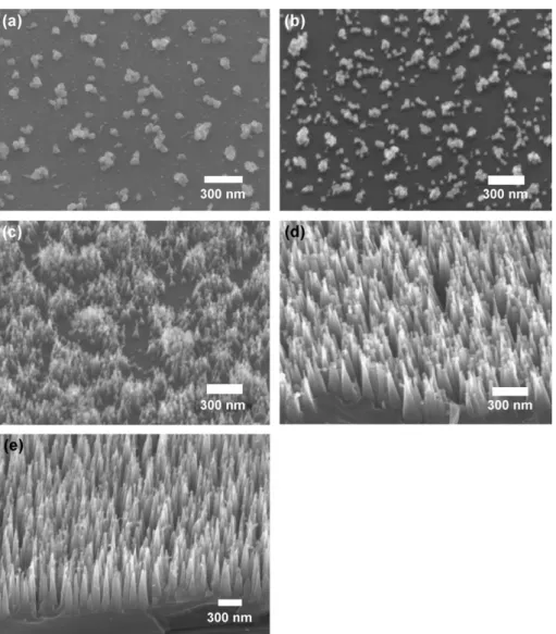
Fig. 1. Typical SEM micrographs of the as-grown CNCs synthesized under different negative substrate bias: (a) 0 V, (b) 50 V, (c) 150 V, (d) 200 V and (e) 300 V (ref. toTable 1).
(I–t curve) measurement, where 900 V bias was applied during the 3600 s of operation.
3. Results and discussion
3.1. Effects of applied bias and H2/CH4ratio on the growth
of CNCs
The effect of the substrate bias on carbon nanostructures was explored by varying bias from 0 to 300 V under the same H2/CH4 ratio (=80/5 sccm/sccm) of the gas sources.
The SEM morphologies of the as-grown nanostructures
under five different bias values are shown inFig. 1(a) to (e), respectively. It indicates that the nanostructures gradually change from polyhedral carbon clusters to needle-like CNCs by increasing the negative substrate bias, and become the well-aligned CNCs at bias N 150 V (Specimen B4 and B5). In other words, the substrate bias is one of the key parameters to form the aligned CNCs. Besides, the average height of the CNCs increases from 20–80 to 500 nm as the applied bias increasing from 150 to 300 V. It implies that a greater negative substrate bias can enhance the growth rate of CNCs perpendicular to the substrate. Furthermore, higher substrate bias may promote to form
Fig. 3. Raman spectrum of the as-grown CNCs (Specimen B5).
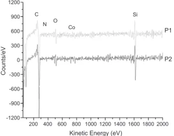
Fig. 4. AES spectra of the as-grown CNCs, where P1 and P2 are sites on individual CNC of the corresponding SEM image inFig. 5(Specimen B5). Fig. 2. Typical SEM micrographs of the as-grown CNCs synthesized under different CH4flow rates at 80 sccm H2: (a) 1, (b) 5, (c) 10 and (d) 15 sccm CH4
the CNCs with sharper tip due to the effect of ions bombardment. This phenomenon is in agreement with the observation of the smaller apex angle at the tips of CNCs, where the apex angles are 15–208 and 9–128 under 200 V (specimen B4) and 300 V (specimen B5) applied bias, respectively.
The SEM morphologies of the as-grown CNCs synthe-sized under different H2/CH4ratios of 80/1, 80/5, 80/10, and
80/15 sccm/sccm are shown inFig. 2(a) to (d), respectively. It indicates the CNCs with a greater average apex angle and larger bottom diameters are deposited under a lower H2/CH4
ratio in gas sources. In other words, the higher concentration of CH4gas may lead to an increase of the lateral growth rate
of CNCs to form a blunt apex angle. The results imply that the nanostructures of CNCs are determined essentially by the competition among etching rate of plasma species, the lateral growth rate and the upward deposition rate of carbon along the surface or through the interior of the catalysts. It is interesting to note that CH4concentration adopted to the
as-grown CNCs in these cases are between the concentrations
for growth of diamond film and CNTs, where diamond film deposition require a lower concentration (H2/CH4=~100/5
sccm/sccm) [15,16]. It is concluded that highly oriented CNCs are more likely to be formed under the appropriate concentration of carbon species in the plasma and higher negative substrate bias.
3.2. Raman and AES analyses of the as-grown CNCs The Raman spectrum of the as-grown CNCs is shown in Fig. 3(Specimen B5). The peak position of the D band and G band are around 1334 and 1598 cm 1, respectively, where the IG/IDratio is ~ 0.81. Huang’s group proposed that a shift
of the E2gG mode from its normal value of 1580 to 1598
cm 1 is an indication of the existence of nanocrystalline graphite or sp2clusters[17–19]. The peak at 1334 cm 1is assigned as A1gmode due to the presence of aromatic rings
in disordered graphite rather than diamond peak at 1332 cm 1. Therefore, the bonding structure of the as-grown CNCs can be considered as sp2 clusters in an amorphous carbon (a:C) matrix.
The AES spectra and the corresponding SEM image of the as-grown CNCs at the tip (P1) and bottom (P2) sites are shown in Figs. 4 and 5, respectively (Specimen B5). The results show detectable signals of carbon, nitrogen, oxygen, cobalt and silicon both on the tip and bottom surfaces of the CNCs. It speculates that the signals of oxygen and nitrogen
Fig. 5. Typical SEM image of the as-grown CNCs, where the arrowheads indicate the selected tip (P1) and bottom (P2) positions on individual CNC.
Fig. 6. The magnified AES spectra ofFig. 4around carbon peak positions.
Fig. 7. The magnified AES spectra ofFig. 4around Co peak positions.
Table 2
FE properties of the as-grown nanostructures synthesized under different negative substrate bias
Specimen designation Applied bias (V) Eturn-onat 10 AA/cm2 (V/Am) Ethresholdat 10 mA/cm2 (V/Am) Current density at 10 V/Am (mA/cm2) B2 50 7.6 not reach 0 B3 150 8.3 not reach 0 B4 200 5.8 8.1 59 B5 300 5.0 7.0 173
may be attributed to absorption from atmosphere during specimen handling. The corresponding AES magnified spectra of Fig. 4 are shown in Figs. 6 and 7 to compare with the reported spectrum [20,21]. It indicates that the peaks of the as-grown CNCs at 252 and 275 eV are belonging to graphite phase. It is also noted that the peaks for Co catalyst at tip area are slightly weaker than at bottom area, implying special growth mechanism combining both base-growth and tip-growth modes.
Moreover, it is interesting to note that the significant Si signal is present in the AES spectra of the as-grown CNCs. First, it may be due to the bias induced Si sputtering from the Si substrate and re-depositing on the surface [22]. Secondly, the diffusion of Si atoms along the CNCs surface from Si substrate may occur [23]. In other words, the nanostructure of the as-grown CNCs is basically consisting of mixture of Co, graphene planes, disordered graphite, amorphous Si and amorphous carbon.
3.3. Field emission properties
The field emission properties of the as-grown CNCs deposited with different negative substrate biases (Speci-mens B2, B3, B4 and B5) are shown inTable 2. It shows that the best FE properties belong to the CNCs by the greatest negative bias ( 300 V, Specimen B5), which is essentially the CNCs of the greatest aspect ratio; where the turn on electric field (Eturn-on), threshold electric field (Eth) and the
current density (at 10 V/Am) are 5.0 V/Am, 7.0 V/Am and 173 mA/cm2, respectively. It is interesting to note that the CNCs at a relative lower negative bias than 300 V show the agglomeration phenomenon of CNCs (Specimen B4 at 200 V bias), which may further decline the FE properties due to screening effect among neighbor CNCs. The current versus time (I–t) curve of the as-grown CNCs at 900 V is used to examine the stability of CNCs during operation, as shown in Fig. 8(Specimen B5). Except the first 5 min, it indicates that the current remains constant for a testing period of 1 h, though it can be stand longer, implying good adhesion between CNCs with the substrate. The rising of
emission current during the first 5 min is due to removal of the loose nanostructures and annealing effect by the intense electric field.
4. Conclusions
By manipulating the H2/CH4ratio and applying sufficient
applied negative bias (R 200 V), the well-aligned CNCs were successfully synthesized by Co-assisted MP-CVD method. The results show that CNCs are basically consisting of mixture of Co particles, graphene planes, disordered graphite, amorphous Si and amorphous carbon. It is found that a greater negative substrate bias can give rise to better-aligned CNCs with sharper apex angle at the tips, better FE properties, greater adhesion with the substrate and better structure stability in electric field. It is also found that the CNCs under 200 V bias has agglomeration phenomenon, which will have a negative effect to FE properties due to screening effect. Under the present conditions, the well-aligned CNCs synthesized under H2/CH4(80/5 sccm/sccm)
ratio, 300 Vapplied bias and 10 min deposition time exhibit good life testing stability and best FE properties: Eturn-on~5.0
V/Am, Eth~7.0 V/Am, and J ~173 mA/cm2at 10 V/Am.
Acknowledgements
This work was supported by the National Science Council of Taiwan under Contract No. NSC92-2216-E-009-010, NSC92-2216-E-009-009, and NSC92-2210-M-009-001.
References
[1] W.B. Choi, D.S. Chung, J.H. Kang, H.Y. Kim, Y.W. Jin, I.T. Ha, Y.H. Lee, J.E. Jung, N.S. Lee, G.S. Park, J.M. Kim, Appl. Phys. Lett. 75 (1999) 3129.
[2] J. Jang, S.J. Chung, H.S. Kim, Appl. Phys. Lett. 79 (2001) 1682. [3] C.L. Tsai, C.F. Chen, C.L. Lin, Appl. Phys. Lett. 80 (2002) 1821. [4] C.J. Huang, Y.K. Chih, J. Hwang, J. Appl. Phys. 94 (2003) 6796. [5] Y.T. Jan, H.C. Hsieh, C.F. Chen, Diamond Relat. Mater. 8 (1999) 772. [6] C.R. Lin, T.J. Wang, K.C. Chen, C.H. Chang, Mater. Chem. Phys. 72
(2001) 126.
[7] G. Zhang, X. Jiang, E. Wang, Science 300 (2003) 472.
[8] Y. Hayashi, T. Tokunaga, T. Soga, T. Jimbo, Appl. Phys. Lett. 84 (2004) 2886.
[9] J.S. Jang, J. Chung, H.S. Kim, Appl. Phys. Lett. 79 (2001) 1682. [10] H.C. Lo, D. Das, J.S. Hwang, K.H. Chen, C.H. Hsu, C.F. Chen, L.C.
Chen, Appl. Phys. Lett. 83 (2003) 1420.
[11] C.L. Tsai, J.H. Hsu, C.F. Chen, Appl. Phys. Lett. 82 (2003) 4337. [12] C.J. Huang, Y.K. Chih, J. Hwang, J. Appl. Phys. 94 (2003) 6796. [13] V.I. Merkulov, A.V. Melechko, M.A. Guillorn, D.H. Lowndes, M.L.
Simpon, Chem. Phys. Lett. 350 (2001) 381.
[14] X.W. Liu, C.H. Lin, L.T. Chao, H.C. Shih, Mater. Lett. 44 (2000) 304. [15] H.L. Chang, C.H. Lin, C.T. Kuo, Diamond Relat. Mater. 11 (2002)
793.
[16] C.M. Hsu, Master Thesis, (2002), Mat. Res. Lab. MSE, NCTU. [17] C.J. Huang, Y.K. Chih, J. Hwang, J. Appl. Phys. 94 (2003) 6796. [18] A.C. Ferrari, J. Robertson, Phys. Rev., B 61 (2000) 14095. Fig. 8. The I–t lifetime testing curve of the as-grown CNCs under 900 V
[19] R.O. Dillon, J.A. Woollam, V. Katkanant, Phys. Rev., B 29 (1984) 3482.
[20] C.R. Lin, T.J. Wang, K.C. Chen, C.H. Chang, Mater. Chem. Phys. 72 (2001) 126.
[21] I.F. Ferguson, Auger Microscope Analysis, IOP, Publishing, Bristol, 1998, p. 63.
[22] X.D. Bai, C.Y. Zhi, S. Liu, E.G. Wang, Z.L. Wang, Solid State Commun. 125 (2003) 185.
[23] W.Y. Yeh, J.Y. Hwang, A.P. Lee, C.S. Kuo, H. Chang, Appl. Phys. Lett. 79 (2001) 3609.