A New Compensation Method for Emission
Degradation in an AMOLED Display Via
an External Algorithm, New Pixel Circuit,
and Models of Prior Measurements
Kuei-Yu Lee, Yen-Ping Hsu, Paul C.-P. Chao, Member, IEEE, and Wei-Dar Chen
Abstract—A new external algorithm with sensing circuit are pro-posed to compensate AMOLED display degradation. The compen-sation is enabled by first evaluating degradation level of OLEDs based on the OLED anode voltages detected by a newly-designed sensing subcircuit. According to sensed voltages, the external al-gorithm selects appropriate built-in models to compensate OLED degradation with the aim to achieve expected OLED emitted lumi-nance. The models are established based on prior measurements to prescribe the relations between luminance and current
and luminance and voltage of each OLED. In this way of compensation, the proposed method is able to incorporate neg-ative effects of OLED degradation aggravation while increasing driving current to compensate the original decay in OLED lumi-nance. Moreover, another algorithm along with the 4T0.5C pixel circuit as presented in prior studies are adopted to compensate process variation in among pixels for improving the emission uniformity of an AMOLED panel. Experiments are conducted by combining the external algorithm with sensing circuit and the pixel circuit to validate the performances of compensating and allevi-ating OLED degradation.
Index Terms—Active-matrix organic light-emitting diode (AMOLED), aggravated degradation, alleviation, compensation.
I. INTRODUCTION
A
CTIVE-MATRIX organic light-emitting diode(AMOLED) displays are largely considered to be the most popular displays of next generation. These have various merits including high brightness, high efficiency, wide viewing angle, and simple structure [1]. Recently, small-sized AMOLED panels are employed in mobile phones. However, for large-sized AMOLED panels, the troublesome drawbacks like OLED degradation and panel non-uniformity still hinder AMOLED displays to replace LCD TVs in the future.
Manuscript received March 14, 2013; revised July 09, 2013 and October 21, 2013; accepted November 16, 2013. Date of publication November 25, 2013; date of current version February 11, 2014. This work was supported in part by the UST-UCSD International Center of Excellence in Advanced Bio-Engi-neering sponsored by the Taiwan National Science Council I-RiCE under Grant NSC-101-2911-I-009-101.
The authors are with the Department of Electrical Engineering, National Chiao Tung University, Hsinchu 300, Taiwan (e-mail: [email protected]. tw).
Color versions of one or more of the figures are available online at http:// ieeexplore.ieee.org.
Digital Object Identifier 10.1109/JDT.2013.2292555
As for OLED degradation, some research works were pro-posed to explore the phenomenon of OLED degradation. The stated causes for degradation are like accumulative holes [2], the impurity of movable ions [3], [4], or the Indium move [5]. All the aboves lead to decay in the organic emitting layer during long-time drives. To remedy the problem, some past works pro-posed the known means of reverse bias [6], [7] to alleviate degradation of a single emitting OLED chip. Another study was later conducted in [8] to propose the application of reverse bias on a 5T1C pixel circuit with a relatively large layout area of the employed pixel circuit. A new 4T0.5C pixel circuit with reverse bias enabled in a smaller layout area was presented in [9] later to increase OLED panel resolution to a required level. Although the OLED degradation was alleviated successfully on the ex-periment results in [8], [9], it still needs a detailed, concrete compensation algorithm to ensure OLED emission to expected luminance levels with inevitable OLED degradation present. Chaji et al. [10] proposed a method to compensate OLED cur-rent to desired value based on sensed curcur-rent, expecting that the OLED emission luminance is compensated. This method however fails to achieve accurate compensation due to possible degradation in OLED emitted luminance with respect to a given current over a long period of operation. Kohno et al. in [11] pro-posed a pixel circuit to improve image-sticking, but it did not ad-dress how to compensate OLED degradation. Lin et al. [12] pro-posed the approaches of current compensation, where the cur-rent through an OLED component was adjusted larger to main-tain originally-designed emitted luminance. These larger cur-rents, however based on basic operation principles of OLEDs, aggravate OLED degradation, leading to a further change in OLED electro-optical behaviors and thus posing greater diffi-culty in compensating OLED degradation. On the other hand, In et al. [13], [14] and Min et al. [15] evaluated the OLED lu-minance degradation by detecting the voltage across the OLED, and then proposed an external algorithm to compensate the lu-minance decay. The degradation evaluation is done based on a measured relation between the OLED anode voltage incre-ments and its normalized luminance. However, the relation is most likely not to be precisely preserved for the OLEDs driven in varied levels of currents for an extensive time of compensa-tions, since the OLED would experience significant changes in electro-optical behaviors [3], [4], leading to possible imprecise compensations.
1551-319X © 2013 IEEE. Personal use is permitted, but republication/redistribution requires IEEE permission. See http://www.ieee.org/publications_standards/publications/rights/index.html for more information.
190 JOURNAL OF DISPLAY TECHNOLOGY, VOL. 10, NO. 3, MARCH 2014
Fig. 1. An external compensation algorithm and the sensing circuit with the 4T0.5C pixel circuit.
To achieve better compensation precisions over a longer pe-riod of OLED compensations, in this study, a large-sized data bank of OLED’s electro-optical models prescribing the rela-tions between luminance and current and luminance and voltage of an OLED is established based on a large amount of prior, off-line measurements and indexed by a newly-defined degradation indicator. During operations, based on these models, a new external compensation algorithm ap-plied to a sensing and 4T0.5C pixel drive circuit [9] is proposed herein to render accurate luminance of an AMOLED panel, even though OLED degradation is possibly aggravated by a number of compensations activated. Note that using the pro-posed method, OLEDs can be compensated to required lumi-nance regardless of degradation status, but paying the price of hardware establishment to execute the compensation algorithm and to store large-scale and models. In addition to degradation compensation, the proposed algorithm with pixel circuit is capable of compensating threshold voltage vari-ation of TFTs in pixels and applying reverse bias to alleviate OLED degradation. Note that variation might lead to dis-play non-uniformity. A number of past studies [16], [17] have worked on similar issues related to variation. Special de-signs in pixel circuit and addressing timing procedure are pre-sented to integrate successfully the functions of compensating aggravated degradation, variation and reverse biases to al-leviate OLED degradation.
The algorithm establishment is described in Section II. In Section III, the experiment is accomplished by the fabricated 4T0.5C pixel circuit operated with the sensing circuit and external algorithm to validate the performances of both com-pensating and alleviating OLED degradation, and variation compensation. Finally, all study conclusions are summed in Section IV.
II. THEALGORITHM
The essence of the external compensation algorithm designed in this study is illustrated by Fig. 1, where the computations by the algorithm are shown in blocks in a red frame, while the rest is the pixel circuits. The algorithm performs jobs of (1) detecting OLED anode voltage to assess its degradation, (2) compensating OLED emission by re-calculating new ’s, (3) sensing variations of TFTs and performing compensation, and (4) ap-plying reverse biases to actively alleviate OLED degradation.
The blocks in the red frame in Fig. 1 include
compensa-tion discriminacompensa-tion, model seleccompensa-tion, model establishment, in-putting gray level, outin-putting reverse bias, calculating vari-ation, and correcting . The required computations in these blocks can be executed by a micro-processor. This processor ac-cepts sensed inputs from the sensing circuit (in yellowish area) in the pixel and converted them to digits via analog-to-digital converters (A/Ds). Note that the sensing circuit detects OLED anode voltages in a given portion of a single-image addressing
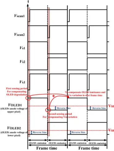
Fig. 2. Timing diagram for the 4T0.5C pixel circuit and sensing circuit.
frame, and then provides the algorithm an indication of OLED degradation level [3], [4]. Based on the sensed OLED anode voltage, the algorithm calculates the corrected ’s to output to the data driver for compensating the OLED degradation and variation. The compensation operation is detailed in the fol-lowing subsections.
A. Operation of Pixel and Sensing Circuit
The pixel circuit at the right side of Fig. 1 illustrates a couple of 4T0.5C pixel circuits in light blue and green and also a sensing circuit in yellow. The 4T0.5C pixel circuits were pre-sented in [9] while the sensing circuit is newly proposed in this study for sensing the OLED degradation level. The associated timing diagram of the pixel circuits is shown in Fig. 2, where two frames are considered to elaborate the compensation algo-rithm. and in both Figs. 1 and 2 represent the scan line signals for the first and second row, respectively. and are the OLED reverse biases applied in the non-emission periods to actively alleviate OLED degradation. is the control signal on switches and to activate/de-activate the sensing function of the designated pixel circuit.
and denote the anode voltages of OLEDs in the upper and lower pixels, respectively, in Fig. 1. As the control signals in Fig. 2 are input into the pixel circuits in Fig. 1, a couple of 4T0.5C pixel circuits operate in a way that emits while
Fig. 3. Circuit operation for sensing in Fig. 1 during the first sensing period.
is in reverse bias period, and vice versa. According to the operation of pixel circuit in [9], this 4T0.5C pixel circuit owns both merits of alleviating OLED degradation by applying reverse bias in the first half of a frame time and maintaining high-resolution display by sharing a capacitor between two adjacent pixels. However, OLED degradation and variation still need to be compensated by an external driving algorithm.
Based on the research works reported in [3], [4], one of the OLED degradation characteristics is that the anode voltage of OLED component inevitably increases for a long-time drive. This increased anode voltage of OLED is sensed in this study to serve as an indicator for a given degradation level of OLED [3], [4]. With mechanism of sensing degradation in hands, the operation on the sensing circuit is next distilled and the associ-ated driving timing diagram is designed and illustrassoci-ated by Fig. 2. In this figure, the anode voltages of two OLEDs, and , are sensed and used to determine the level of OLED degradation. To elaborate the sensing mechanism, the partial pixel circuit associated with as shown in Fig. 3 is con-sidered to describe the operation of sensing circuit during the first sensing period in Fig. 2. In this period, according to the op-eration of pixel circuit in [9], in Fig. 3 emits, while is in reverse bias period. Meanwhile, in the sensing circuit, and are operated at the low and high level, respectively. The anode voltage of , , is sensed to a buffer as
(1) On the other hand, and are operated at the low level to charge in order to sense the anode voltage of , . The procedure is utilized to acquire the variation of
, , in the reverse bias period of as shown
in Fig. 2. The details of compensation are described in sub-sequent Section II-G.
The sensing results, and , are then utilized in the following algorithm blocks to process the compensation procedures.
192 JOURNAL OF DISPLAY TECHNOLOGY, VOL. 10, NO. 3, MARCH 2014
B. Compensation Discrimination Block
In this block, the sensed anode voltage of , , is utilized to serve as the degree of OLED degradation according to the equation defined by
(2) which is in fact an error ratio of voltage compensation between the sensed voltage of OLED anode, , and the expected
voltage of OLED anode, . This is
obtained from a model established based on prior measurements in an off-line fashion. The compensation and prior measure-ment procedures are detailed in the subsequent Sections II-D and II-E, respectively. Via calculating (2), the degree of OLED degradation can be determined. The calculation results are input into the block of Model Selection, as shown in Fig. 1, in order to select an appropriate compensation model for maintaining the OLED luminance to expected levels.
C. Model Selection Block
The computation associated with this block is to select the appropriate compensation model after successfully evaluating OLED degradation degree as stated in the compensation
dis-crimination block. The models include the correspondences
from luminance to current and from luminance to voltage . For example, as shown in Model selection block in Fig. 1, a% and b% represent varied ratios of anode voltage error, , in (2). As the anode voltage of degra-dation OLED increases, exceeding certain listed ratios, e. g. a% or b%, the selected model is changed from A to B or B to C, respectively, for compensating OLED emission. To build up the entire model bank, appropriate ranges of ratios, , are first determined to cover realistic operations of fabricated OLEDs. These ranges depend on required display brightness, different OLED devices/fabrications, the capability of data driver, and required capacity of model density for computation accuracy.
D. Blocks of Model Establishment and Inputting Gray Level
The computation in Model establishment block in Fig. 1 in-tend to establish two associated model curves of and , where , , and are gray level, compensated driving current, and expected voltage of OLED anode, respectively. Note that the compensation on OLED degradation executed by this block is made possible with the required gray levels for a given image input from the inputting gray level block, also shown in Fig. 1. Based on the models of and provided and selected by blocks of Model Establishment and Selection, respectively, the desired OLED compensating current, , can be calcu-lated. With this current, the proposed algorithm in the block of
Model Establishment further calculates required input data-line
voltage based on designed pixel circuit, which is achieved by solving the governing equation of the drive TFT for , i.e.,
(3)
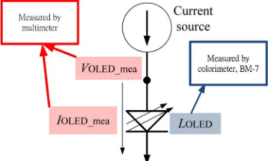
Fig. 4. Measurement for establishing OLED models.
where incorporates mobility, gate capacitor , and the aspect ratio of driving TFT. is the threshold-voltage of the driving TFT. is the corresponding data-line voltage. calculated by (3) is obtained and output to the correcting block as also shown in Fig. 1. Note that the block also accepts correction on for varia-tion compensavaria-tion. The related details are given in subsequent Section II-G. As shown in Fig. 1, the compensated results of
OLED degradation and variation, and , are
finally summed to output the data-line voltage, . It should be noted at this stage that the established curves provides the expected voltage of OLED anode, , to eval-uate OLED degradation degree again in each frame time. As shown in the curve of Fig. 1, the required gray level of this frame time is also set by inputting gray level block, while
curve output corresponding to
compen-sation discrimination block. Then, is sensed to calculate with the for discriminating degradation degree again. Therefore, the degradation compensation procedures can be processed in each frame time repeatedly for realizing the on-line sense in each pixel.
E. Models Based on Prior Measurement
Flskdac;laskc’;as’l;kmc;aksmjclkanmsml;ck;lasknclaskn-clasnclaslcnlasncl;nasckasjchkljasklcjlkasjcnblksclkaThe aforementioned curves of and are established by prior off-line measurements. is set to be equal to measured OLED anode voltages, . The process to build a large-sized database of prior measurements for establishing curves of and are detailed in this subsection.
The setup for acquiring prior measurements includes a cur-rent source and an OLED component as shown in Fig. 4. In this figure, denotes the anode voltage of the OLED, while is the driving current generated from an as-sumed current source, which are all recorded by a multi-meter in the measurement process. is the luminance emitted by the OLED, which is recorded by a colorimeter, BM-7. Two curves, and , are recorded for varied OLED drive currents. Resulted measurements are in fact used to affirm the
relations among , , and . Note that
as previously defined, the level of OLED degradation is evalu-ated and indicevalu-ated by the anode voltage of OLED, . During measurement, the OLED is allowed to be driven for an extensive period of time for the presence of OLED degradation,
Fig. 5. Compensation on an OLED in a panel with degradation aggravation.
until the degradation level pre-defined in (2) reaches pre-desig-nated values, say a%, b%, , etc. Between these pre-designated ratios, local models of and can successfully be estab-lished, as denoted by Model A, B, ., etc, in blocks of Model
Establishment and Selection in Fig. 1. In practice, the discrete
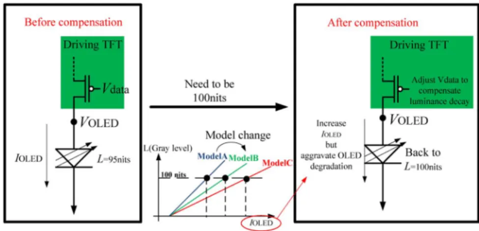
measurement data for prescribing these local models are stored into the memory for use. In operations of an AMOLED display panel, as OLEDs degrade, the data driver selects the appropriate local model based on the sensed anode voltage of OLED, and then output the corrected data voltage for compensating OLED luminance decay. Fig. 5 illustrates aforementioned compensa-tion process on an OLED.
It should be noted that as shown in Fig. 5, the OLED current, , is increased in operation to compensation degradation for achieving required emitted luminance. This increased OLED current however aggravates degradation based on fundamental principles of OLEDs, in fact resulting in an extra increase in . Fig. 6(a) illustrates the realistic evolution of as the OLED is compensated for required luminance. In this figure, between X and Y or Z and U, local models A or B are employed, respectively, for predicting behaviors of the driven OLED. The corresponding instant at Y is when the OLED degradation indi-cator, , exceeds prescribed a% and compensation has to be executed. The compensation in fact increases the OLED current by the amount calculated by local model A in order to deal with degradation to achieve desired emitted luminance. The anode voltage of the OLED thus appears in a certain jump at the point Y when the OLED current is increased deliberately for compensation.
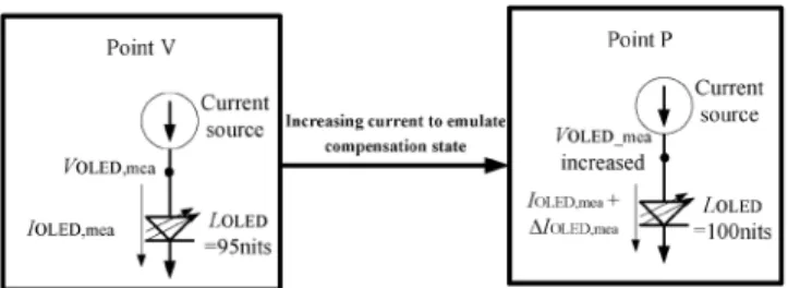
Fig. 6(b) illustrates the evolution of OLED anode voltage when establishing the model by a special method based on prior measurement, where represents the anode voltage of OLED in the measurement procedure of Fig. 4. The point represents the moment of recording initial and curves of model A. After increasing a% voltage as calculated in (2), and curve of model B are recorded at the moment of point . The blue dashed line represents the prior measurement without adjusting current source for emulating the compensation state, where point is the moment to record and curves of model C, obviously. However, according to the typical voltage history at OLED anode in Fig. 6(a), the anode voltage needs to be raised to maintain luminance just like the
Fig. 6. (a) Typical voltage history at OLED anode during compensation. (b) Local model establishment based on measurement.
point is changed to point . Therefore, the degradation curve of prior measurement also needs to be changed to follow the green solid line, since the compensation procedures aggravate OLED degradation. Consequently, adjusting the current source of Fig. 4 after each prior model establishment for emulating typ-ical anode voltage history is designed. For example, in Fig. 7, after recording model B at point , the current of prior measure-ment in Fig. 4, , is increased to maintain 100 nits lu-minance emulating the compensation procedures in Fig. 5. The degradation curve of local model measurement after recording model B is hence corrected to be green solid line as shown in Fig. 6(b). When voltage error ratio increases exceeding b%, model C is recorded at point rather than point , since the special method based on prior measurement emulate the aggra-vated OLED degradation. The local models are also recorded
194 JOURNAL OF DISPLAY TECHNOLOGY, VOL. 10, NO. 3, MARCH 2014
Fig. 7. Compensation activated with aggravated OLED degradation considered.
continually until they satisfy compensation requirements. Fol-lowing this method, the required local models of external algo-rithm do not need to be established according to the various and complicated mathematical equations as using the diverse OLED devices. Even though the compensation state aggravates OLED degradation, this special method based on prior measurement can also achieve accurate compensation.
F. Outputting Reverse Bias Block
The Outputting reverse bias block as illustrated in Fig. 1 out-puts the required reverse biases to the pixel circuit for allevi-ating OLED degradation. Appropriate levels of reverse are se-lected for satisfactory effects of easing OLED degradation [6]. This reverse bias is applied to one pixel as shown in Fig. 2 in the emission period of another pixel in each display frame time.
G. Blocks of Calculating Variation and Correcting
During the sensing period in each display frame, as illustrated in Fig. 2, the variation is sensed and compensated by subse-quent related calculations. The associated works are in the block of Calculating variation and Correcting in Fig. 1. Since the operations of sensing variations in upper or lower pixels are identical, the details of Calculating variation is
described herein only for in the lower pixel.
As illustrated in Fig. 3, the switches of and are controlled by and , respectively. During the reverse bias period of in Fig. 2, is cut off, while the anode voltage of , , is at the reverse bias level by ap-plied appropriate . Therefore, when charging until the
steady state, becomes
(4) where denotes the sensed low-voltage level of . This charging result is then input into the external compensation algorithm through a buffer and sensing analog-to-digital con-verters (A/Ds) as shown in Fig. 1. The block of Calculating
variation next calculates the sensed to obtain required variation information as
(5) where is obtained from the operations of the Outputting
reverse bias block. Combination of (4) and (5) leads to
(6)
where is obviously equal to . Therefore,
can be derived by
(7) where represents the sensed threshold voltage of , as enabled by the operation in Fig. 3. The derived is next used to modify the OLED data-line voltage for compensa-tion by
(8) where is the final data-line voltage with compensation on both OLED degradation and variation. Note that the proposed degradation compensation process is detailed in Section II-D. in (8) is output to data line and the resulted driving current for the designed pixel can be derived based on basic circuit theory as
(9) where consists of mobility, gate capacitor , and the aspect ratio of the driving TFT. is the threshold of the driving TFT. It is seen in (9) that if is close to , the variation is canceled in the current equation. In this way, the OLED luminance degradation is compensated by , as evident in (9).
To explore the performance of compensating OLED degrada-tion and variation by the proposed design, the 4T0.5C pixel is fabricated to work with the proposed external compensation algorithm operated on a field programmable gate array (FPGA) module.
III. EXPERIMENTVALIDATION
A. Model Establishment
The model establishment for use by the external algorithm is conducted following the operations illustrated by Figs. 4 and 7. The detailed steps are given in Section II-E. Note that since the anode voltage of OLED increases in a highly-nonlinear and un-predictable fashion, the error ratios defined in (2), , are designated corresponding to 20% drops in OLED emitted lumi-nance, which are 8.54% for model-switching between model A and model B, and 2.57% for model-switching between model B and model C, for a test 14-in AMOLED display in labora-tory. Exemplary measurement results of local and curves are shown in Fig. 8(a) and (b). Using these curves, the external algorithm is able to output the appropriate and for required gray levels (luminances), the process of which is included in Fig. 1. Note herein that the aforemen-tioned designated 20% drops can be easily devised to smaller levels to establish finer local models of and . The related experimental results of compensation are presented in Section III-D.
B. Experimental Setup and Process
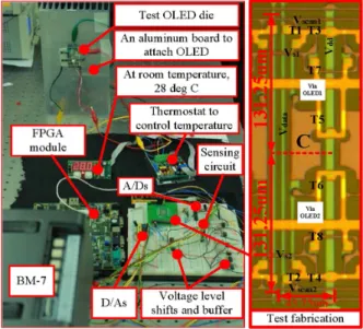
The experiment system is shown by a photograph in Fig. 9. The low-temperature poly silicon (LTPS) TFTs fabricated by
Fig. 8. Local models of (a) and (b) curves.
Fig. 9. Experiment system.
excimer laser annealing (ELA) are employed herein to fabri-cate the proposed 4T0.5C pixel [9]. To investigate the varied experimental performances including OLED degradation com-pensation and alleviation, and rule out the effects of temperature on OLED luminance, a system set with a drive circuit with ad-equate power for 100 pixels is orchestrated and wire-bonded to a single test OLED die in . The OLED die is at-tached at the bottom of an aluminum board in order to control at room temperature, 28 deg C, using a commercialized con-trol unit and based on the feedback signals from a thermostat. A colorimeter BM-7 is utilized to measure the OLED luminance. Note that using a single OLED die for experiment herein could
Fig. 10. Experiment setup for compensation by implementing the external compensation algorithm to a fabricated test panel.
obtain measurement data slightly different from a large-sized panel due to known IR-drop phenomenon [18]. However, the main focus of the current work is on the effectiveness of the proposed emission compensation algorithm, not the size effect of a panel.
The experiment process for compensation is illustrated in
Fig. 10, where and curves are embedded into a
FPGA module via forging a code in Verilog hardware descrip-tion language (HDL). In this code, a frequency divider written by Verilog HDL is designed to output required 60 Hz signals, , , , , and , from the clock generator in the FPGA module. and are set to be dc voltages of 6 V and 5 V, respectively. The scan line signals, , , and all range from 5 to 10 V, while enabling signals of reverse bias, and , are set from 10 to 10 V according to the required reverse bias. Digital-to-analog converters (DACs) and analog-to-digital converters (ADCs) are used for signal trans-formations. Buffers and voltage level shifts are used to adjust voltage levels to conform to requirement of the FPGA module and pixel circuit.
C. Compensating Variation
The experiment for validating compensation is conducted by using two test pixel circuits, named A and B. Without com-pensation by the external algorithm, the luminance curves are measured, further normalized by maximums, and then shown in Fig. 11(a). It is seen from this figure that differences in OLED lu-minance is present with average of 17.8% between test pixels A and B.
On the other hand, Fig. 11(b) shows the experiment results with compensation enabled. In this figure, lower difference in OLED emitted luminance is obtained with compensation. The difference is reduced from previous 17.8% to 3.2%. This reduction in emission difference validates well the expected performance of compensating variation due to fabrication process.
D. Compensating and Alleviating OLED Degradation
In addition to handle variation, the main function of the proposed pixel circuit along with the external algorithm is to compensate and alleviate OLED degradation by established
196 JOURNAL OF DISPLAY TECHNOLOGY, VOL. 10, NO. 3, MARCH 2014
Fig. 11. Experiment results in luminance for varied gray levels; (a) without compensation and (b) with compensation.
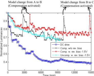
Fig. 12. Experiment results of compensating OLED degradation.
local models and reverse biases, respectively. Experimental results are summarized and shown in Fig. 12. The data are collected for an extensive period of time. Four cases of data with are presented in this figure. One presents the data for an OLED biased by a DC drive. Since the storage capacitance in a typical 2T1C circuit is often designed to be charged to steady state in a very short period of time as compared to the whole frame time, the OLED component in the 2T1C pixel circuit can be regarded in emitting status in the full frame time. Therefore, the wire-bonded DC drive in Fig. 12 can be regarded almost equivalent to the drive by 2T1C pixel circuit. The other two apply the compensation methods proposed with two different biases of 0 and 1.5 V, i.e., without and with reverse biases enabled in the half current-off period illustrated by Fig. 2 in a addressing frame of an OLED panel. The last one presents un-compensated luminances but with reverse 1.5 V for comparison.
It is seen from Fig. 12 that the proposed OLED degradation compensation is automatically activated twice for each of the two cases with 0 and 1.5 V as reverse biases. At the four in-stants of compensation activated, the OLED emitted luminances are elevated back to original-required normalized luminance of one, showing the very effectiveness of the proposed pixel cir-cuit, the external compensation algorithm and local models of and established. Note that the 20% degradation during operation is due to the fact that the OLEDs continue to
degrade between the employments of different OLED models. This 20% is actually set by the designer based on the mecha-nism proposed in this study. It can be set much smaller (like 5% or even any given smaller value), with a larger set of , OLED models to be established and more frequent em-ployments of new, different models during operations. Further-more, the luminance curve with DC drive representing 2T1C circuit shows serious luminance decays as compared to other two cases with compensation, indicating the necessity of ap-plying the compensation proposed. It is also shown in this figure that the luminance decay of the curve with reverse bias applied (red) is slower than the one (black) without reverse bias, demon-strating well the favorable performance of proposed method of reverse bias. Finally, another curve shown in this figure con-tains uncompensated OLED luminances with reverse bias 1.5 V, which are shown clearly lower than the compensated curve after the first compensation for an extensive period of time, even with the accelerated drops right after the compensations applied each time. This demonstrates well the improvements offered by the proposed compensation method not only in emitting correct luminance right at compensations but also leading to smaller lu-minance errors afterward based on corrected, new models. Note that accelerated, exponential-like drops are always present upon a sudden increase in OLED current which complies with the basic emission microelectronic physics of OLEDs [19].
IV. SUMMARY
An external OLED compensation algorithm along with a pixel sensing/addressing circuit is designed successfully. The algorithm is capable of offering the applied voltage to achieve a given emitted luminance with consideration of OLED degradation. This is made possible by establishing two groups of data-base models for predicting relations between emitted luminance and voltage/current of the OLED based on a large amount of off-line measurements. Methods of model measurements are designed to emulate possible aggravated degradation of OLED for the more accurate compensation. The models are further extended to those for the cases as OLED degradation amounts to higher levels. On the other hand, the designed pixel circuit provides a chance to estimate the OLED degradation level in an on-line fashion by sensing OLED voltage within a selected short time span in a typical image frame time. With sensed OLED voltages, one is able to choose the correct data-based models of luminance-current to perform compensation. A test pixel is fabricated and driven with the sensing circuit and established compensation algorithm. Exper-imental results show that the compensation is effective in the evidence of displaying desired OLED luminance. Moreover, variation is also shown compensated effectively and the applied reverse bias is able to alleviate OLED degradation.
ACKNOWLEDGMENT
The authors would like to thank AU Optronics Corporation, Hsinchu, Taiwan, for their assistance in fabricating the OLED pixel circuit for testing and appreciate the support from National Chip Implementation Center.
REFERENCES
[1] C. Hosokawa, M. Matsuura, M. Eida, K. Fukuoka, H. Tokailin, and T. Kusumoto, “Full-color organic EL display,” J. SID, vol. 6, no. 4, pp. 257–260, 1998.
[2] D. Y. Kondakov, J. R. Sandifer, C. W. Tang, and R. H. Young, “Nonradiative recombination centers and electrical aging of organic light-emitting diodes: Direct connection between accumulation of trapped charge and luminance loss,” J. Appl. Phys., vol. 93, no. 2, pp. 1108–1119, Jan. 2003.
[3] J. Shen, D. Wang, E. Langlois, W. A. Borrow, P. J. Green, C. W. Tang, and J. Shi, “Degradation mechanisms in organic light emitting diodes,”
Synth. Metals, vol. 111, pp. 233–236, 2000.
[4] M. Hack, J. J. Brown, J. K. Mahon, R. C. Kwong, and R. Hewitt, “Per-formance of high-efficiency AMOLED displays,” J. SID, vol. 9, no. 3, pp. 191–194, 2001.
[5] S. T. Lee, Z. Q. Gao, and L. S. Hung, “Metal diffusion from electrodes in organic light-emitting diodes,” Appl. Phys. Lett., vol. 75, no. 10, pp. 1404–1406, Sep. 1999.
[6] M. Yahiro, D. Zou, and T. Tsutsui, “Recoverable degradation phe-nomena of quantum efficiency in organic EL devices,” Synthet. Metals, vol. 111, pp. 245–247, Jun. 2000.
[7] Y. J. Si, L. Q. Lang, Y. Zhao, X. F. Chen, and S. Y. Liu, “Improve-ment of pixel electrode circuit for active-matrix OLED by application of reversed-biased voltage,” IEEE Trans. Circuits Syst. II, Exp. Briefs, vol. 52, no. 12, pp. 856–859, Dec. 2005.
[8] K. Y. Lee and C. P. Chao, “A new AMOLED pixel circuit with pulsed drive and reverse bias to alleviate OLED degradation,” IEEE Trans.
Electron Devices, vol. 59, no. 4, pp. 1123–1130, Apr. 2012.
[9] K. Y. Lee, Y. P. Hsu, and C. P. Chao, “A new 4T0.5C AMOLED pixel circuit with reverse bias to alleviate OLED degradation,” IEEE
Elec-tron Device Lett., vol. 33, no. 7, pp. 1026–1024, Jul. 2012.
[10] G. R. Chaji, C. Ng, A. Nathan, A. Werner, J. Birnstock, O. Schneider, and J. Blochwitz-Nimoth, “Electrical compensation of OLED lumi-nance degradation,” IEEE Electron Device Lett., vol. 28, no. 12, pp. 1108–1110, Dec. 2007.
[11] T. Kohno, H. Kageyama, M. Miyamoto, M. Ishii, N. Kasai, N. Nakamura, and H. Akimoto, “High-speed programming architec-ture and image-sticking cancellation technology for high-resolution low-voltage AMOLEDs,” IEEE Trans. Electron Devices, vol. 58, no. 10, pp. 3444–3452, Oct. 2011.
[12] C. L. Lin and Y. C. Chen, “A novel LTPS-TFT pixel circuit com-pensating for TFT threshold-voltage shift, OLED degradation for AMOLED,” IEEE Electron Device Lett., vol. 28, no. 2, pp. 129–131, Feb. 2007.
[13] H. J. In and O. K. Kwon, “External compensation of nonuniform elec-trical characteristics of thin-film transistors and degradation of OLED devices in AMOLED displays,” IEEE Electron Device Lett., vol. 30, no. 4, pp. 377–379, Apr. 2009.
[14] H. J. In, K. H. Oh, I. Lee, D. H. Ryu, S. M. Choi, K. N. Kim, H. D. Kim, and O. K. Kwon, “An advanced external compensation system for ac-tive matrix organic light-emitting diode displays with poly-Si thin-film transistor backplane,” IEEE Trans. Electron Devices, vol. 57, no. 11, pp. 3012–3019, Nov. 2010.
[15] U.-G. Min, H.-J. In, and O.-K. Kwon, “A real time video data adjusting method for active matrix organic light emitting diode displays with high image quality,” IEEE Trans. Consumer Electron., vol. 55, no. 4, pp. 2372–2376, Nov. 2009.
[16] S. H. Jung, W. J. Nam, and M. K. Han, “A new voltage-modulated AMOLED pixel design compensating for threshold voltage variation in poly-Si TFTs,” IEEE Electron Device Lett., vol. 25, no. 10, pp. 690–692, Oct. 2004.
[17] J. H. Lee, W. J. Nam, S. H. Jung, and M. K. Han, “A new current scaling pixel circuit for AMOLED,” IEEE Electron Device Lett., vol. 25, no. 5, pp. 280–282, May 2004.
[18] M. H. Jung and O. Kim, “Voltage distribution of power source in large AMOLED displays,” J. Kor. Phys. Soc., vol. 48, pp. S5–S9, Jan. 2006. [19] B. M. Weon, S. Y. Kim, J.-L. Lee, and J. H. Je, “Evolution of luminance by voltage in organic light-emitting diodes,” Appl. Phys. Lett., vol. 88, 2006, Art. ID 013503.
Kuei-Yu Lee received the B.S. degree in electrical
engineering from the National Taiwan Ocean Uni-versity, Keelung, Taiwan, in 2007, and the M.S. and Ph.D. degrees in electrical control engineering from National Chiao Tung University, Hsinchu, Taiwan, in 2009 and 2012, respectively. His research inter-ests focus on thin-film transistors and active-matrix organic light-emitting diode (OLED) display.
Yen-Ping Hsu received the B.S. degree from
Na-tional Chiao Tung University, Hsinchu, Taiwan, in 2009, and the M.S. degree in electrical control engineering from National Chiao Tung University, Hsinchu, Taiwan, in 2011. His research interests focus on active-matrix organic light-emitting diode (OLED) display.
Paul C.-P. Chao (M’07) received the B.S. degree
from National Cheng-Kung University, Tainan, Taiwan, in 1989, and the M.S. and Ph.D. degrees from Michigan State University, USA, in 1993 and 1997, respectively. He worked for the CAE department of Chrysler Corp in Auburn Hill, Detroit, MI, USA, for two years. He is currently a faculty member of the electrical engineering department at National Chiao Tung University (NCTU), Taiwan. In recent years, his research interests focus on interface analog circuit design for optical devices/systems, micro-sensors and actuators.
Prof. Chao was the recipient of the 1999 Arch T. Colwell Merit Best Paper Award from Society of Automotive Engineering, Detroit, USA; the 2004 Long-Wen Tsai Best Paper Award from National Society of Machine Theory and Mechanism, Taiwan; the 2005 Best Paper Award from National Society of Engineers, Taiwan; and the 2002/2003/2004 CYCU Innovative Research Award; 2006 the AUO Award; 2007 the Acer Long-Term 2nd-prize Award; The 2007/2008/2009 NCTU EEC Outstanding Research Award; the 2009 Best Paper Award from the Symposium on Nano-Device Technology; the 2010 Best Paper Award from the 20th Annual IEEE/ASME Conference on Information Storage and Processing Systems (ISPS). He was the Associate Provost of NCTU, the Secretary of IEEE Taipei Section, 2009–2010, and currently the founding chair of local chapter for the IEEE Sensor Council and an AdCom member of the IEEE Sensors Council. He is also the Associate Editors of three well-known SCI-index journals, IEEE SENSORSJOURNAL, ASME Journal of
Vibration and Acoustics and Journal of Circuits, Systems and Computers. He
is an ASME fellow.
Wei-Dar Chen received the B.S. degree in 2003
from Hsiuping University of Science and Tech-nology, Taichung, Taiwan, in 2009, and the M.S. degree in electrical engineering from I-Shou Uni-versity, Kaohsiung, Taiwan, in 2005. Currently, he is working towards the Ph.D. degree in electrical control engineering from National Chiao Tung University, Hsinchu, Taiwan. His research interests focus on photovoltaic control system and battery charging system.