具有臨界電壓補償功能雙閘極 IGZO TFT 電路
之研究
Study on the Dual Gate IGZO TFT Circuits with
Threshold Voltage Compensation Function
研究生 : 盧冠銘 Student: Kuan-Ming Lu
指導教授 : 戴亞翔 博士 Advisor: Dr. Ya-Hsiang Tai
國立交通大學
顯示科技研究所碩士班
碩 士 論 文
A Thesis
Submitted to the Display Institute
College of Electrical and Computer Engineering
National Chiao Tung University
具有臨界電壓補償功能雙閘極 IGZO TFT 電路
之研究
研究生: 盧冠銘 指導教授: 戴亞翔 博士
國立交通大學顯示科技研究所碩士班
摘要
非晶矽 IGZO 薄膜電晶體 (IGZO TFTs) 備受關注,因為它有幾個優點,如高 載子遷移率,高透明度,製程溫度低,均勻性好。然而,臨界電壓 (Vth) 的不 穩定,限制了 IGZO 在電路上的應用。最近,雙閘極 IGZO TFT 被提出具有較好 的元件特性和較穩定的臨界電壓,它的結構分別在底部和頂部各有一個閘極。 在正常的底部閘極 (bottom-gate) 的操作下,雙閘極 IGZO 薄膜電晶體的臨界 電壓可透過頂部閘極 (top-gate) 來操控。基於這個現象,我們提出了透過頂部 閘極的操作來補償臨界電壓的變異的新概念。在本篇論文中,將此新概念應用到 數位緩衝器(digital buffer) 和有機發光二極體(OLED) 的畫素電路中,利用實 驗的方式來驗証這個新概念。Study on the Dual Gate IGZO TFT Circuits with
Threshold Voltage Compensation Function
Student: Kuan-Ming Lu Advisor: Dr. Ya-Hsiang Tai
Display Institute,
National Chiao Tung University
Abstract
Amorphous InGaZnO4 (IGZO) thin film transistor (TFT) has drawn great
attention because it has several merits such as high mobility, high transparency, low processing temperature, and potentially good uniformity. However, the threshold voltage (Vth) instability IGZO TFT can limits its applications in the circuits. Recently, the dual-gate IGZO TFT with two gates on the bottom and the top was proposed to have better device performance and better stability of Vth after voltage stress.
The threshold voltage of the TFT using the bottom-gate in its normal operation can be controlled by the top-gate. Based on this phenomenon, a new concept of using the top-gate to compensate threshold voltage variation is proposed. In this thesis, this
Acknowledgements
在二年的研究所生活中,第一個要感謝的對象是我的指導教授 戴
亞翔博士,老師積極認真的研究態度、講求效率的處事原則及謹慎周
全的思慮,是我除了研究之外,認為最需要向老師學習的項目。感謝
老師總是不厭其煩的提醒我們、指導我們,並且在我們的研究上提供
了許許多多的想法,讓我受益良多。在此,對我敬愛的老師致上最誠
摯的謝意。
此外,還要感謝小瓜呆,在我遇到困難時,時常提供我知識上的
協助。感謝陪伴我這二年的同學政哲和寬寬,讓這二年多了很多歡笑
和趣味。也要感謝學弟們:政達、柏成、承閔的幫忙,以及隔壁實驗
室的佐哥、金剛、ping 和立勛,讓我的碩士生活過的很精彩。
最後,非常感謝我的家人和女友,這段時間給我的支持與鼓勵,
讓我能無後顧之憂的完成這個碩士學位,在此對你們送上我的感謝。
Contents
Chinese Abstract
………...…….
I
English Abstract
.……….…...………..…….
II
Acknowledgement
……...………
III
Contents
……….
IV
Figure Captions
...
VI
Chapter 1 Introduction
1.1 Background ……….1
1.2 Motivation ………...…2
1.3 Thesis Organization
………4
Chapter 2 Digital Buffer
2.1 Peripheral Circuit ………..12
2.2 Vth Compensation ……….12
2.2.1
Reference Circuit
……….12
3.2.1.2 Experimental Result ………...25
3.2.2 5T2C circuit ………25
3.2.2.1 Schematic and Operation
………25
3.2.2.2 Experimental Result
………...26
3.3 Pixel Circuits of Normal
OLED
………...27
3.3.1 4T2C circuit
……….28
3.3.1.1 Schematic and Operation
………28
3.3.1.2 Experimental Result
………...29
3.4 Summary
………..29
Chapter 4 Conclusions and Future Works
4.1 Conclusions
………...40
4.2 Future Works
……….40
Figure Captions
Chapter 1
Fig 1.1 AMOLED pixel circuits ………...6 Fig 1.2 (a) Id–Vbg transfer characteristics of the dual gate TFT under three
different measurement conditions ….…...…...………8 Fig 1.2 (b) Time evolution of Vth during PBTS , NBTS, and NBITS of dual gate
and single gate a-IGZO TFTs …...………...8 Fig 1.3 (a) Cross-section and circuit symbol of dual gate a-IGZO TFT ………...9 Fig 1.3 (b) Id–Vbg transfer characteristics of the dual gate TFT under five
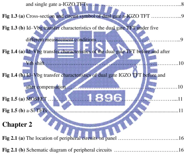
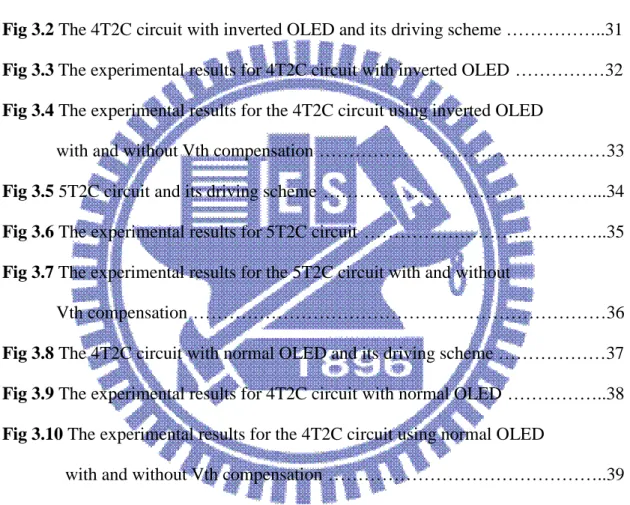
different measurement conditions ………...9 Fig 1.4 (a) Id–Vbg transfer characteristics of the dual gate TFT before and after
Vth shift ……….10 Fig 1.4 (b) Id–Vbg transfer characteristics of dual gate IGZO TFT before and
after compensation ………10 Fig 1.5 (a) MOSFET ………...…………
...
11 Fig 1.5 (b) a-Si TFTs ……...11Chapter 2
Fig 2.7 Comparison of Vin @ Vout equal 5V with and without compensation ……..21 Fig 2.8 Id–Vbg transfer characteristics of the dual gate TFT before and after
voltage stress ………...22 Fig 2.9 Transfer curve of simple and proposed digital buffer before and after
voltage stress ………….………..22
Chapter 3
Fig 3.1 (a) Structure of normal OLED (b) Structure of inverted OLED ………30 Fig 3.2 The 4T2C circuit with inverted OLED and its driving scheme ………..31 Fig 3.3 The experimental results for 4T2C circuit with inverted OLED………32 Fig 3.4 The experimental results for the 4T2C circuit using inverted OLED
with and without Vth compensation………33 Fig 3.5 5T2C circuit and its driving scheme ………...34 Fig 3.6 The experimental results for 5T2C circuit ………..35 Fig 3.7 The experimental results for the 5T2C circuit with and without
Vth compensation ………36 Fig 3.8 The 4T2C circuit with normal OLED and its driving scheme ………37 Fig 3.9 The experimental results for 4T2C circuit with normal OLED ………..38 Fig 3.10 The experimental results for the 4T2C circuit using normal OLED
Chapter 1
Introduction
1.1
Background
The active-matrix organic light-emitting diode (AMOLED) display is a strong candidate for the next-generation flat panel display (FPD) because of its excellent color characteristics, wide viewing angle, high contrast, and low power consumption.
Since OLED is the current-controlled display device, the performances (particularly the stability and uniformity) of the driving thin-film transistors (TFTs) are very important to achieve uniform brightness. The low-temperature polycrystalline silicon (LTPS) TFTs show high mobility and good stability, however the uniformity is typically not acceptable for the AMOLED operation. The hydrogenated amorphous silicon (a-Si:H) TFTs has good uniformity, but the low mobility and poor stability also make it hardly applicable in AMOLED. Alternatively, TFTs with oxide semiconductors, particularly amorphous InGaZnO4 (IGZO),composed of heavy-metal cations with specific electronic configurations
have been widely investigated recently due to their several merits such as high mobility, high transparency, low processing temperature, and potentially good uniformity. All these merits
Owing to the high mobility, IGZO TFTs can also be used to make the peripheral circuits monolithically. However, IGZO TFT is typically in depletion type, which means there is a high leakage current when the gate voltage is zero. Several proposals have been made to solve this problem. [5] Moreover reliability of peripheral circuits for driving cannot be ignored, so various structures of circuit have been developed to conquer this problem, and prevent that affects the function of circuit. [6, 7]
1.2
Motivation
The Vth instability of IGZO TFT can limits its applications in the circuits. Recently, the dual-gate IGZO TFT with two gates on the bottom and the top was proposed to have better device performance and better stability of Vth after voltage stress, the results are shown in Fig.1.2 [8, 9]
Fig.1.3(b) shows the curves of drain current (Id) versus bottom-gate voltage (Vbg) for the dual-gate IGZO TFT at different top-gate voltages (Vtg), with the schematic cross section and circuit symbol of the device in shown Fig1.3(a). These transfer curves exhibit parallel shifts with respect to different Vtg values. This phenomenon is attributed to attraction and expelling of free carriers in the active layer by the top-gate. It implies that, using the bottom-gate of the dual-gate IGZO TFT as the primary gate, Vth can be controlled by the top-gate. This gives us a new idea of using it for the Vth compensation in the circuits. When Vth of the Id-Vbg curve is positively shifted, a negative Vtg can move it back, and vice versa. In other words, by appropriately setting the voltage on the top-gate, the circuit of TFT using the bottom gate can get rid of the problem of Vth shift.
A new concept of Vth compensation can be developed by using this concept with the dual gate IGZO TFTs. Initially we fix Vtg of dual gate IGZO TFT. If Vth shift, we can compensate the variation of Vth by adjusting the Vtg. We take an example to explain the new concept of
Vth compensation, using dual gate IGZO TFT. Fig 1.4(a) shows Id–Vbg transfer characteristics of the dual gate TFT before and after Vth shift. Because top-gate can control the Vth of transistor, we can increase the Vtg to compensate the variation of Vth,vice versa. Fig 1.4(b) shows the Id–Vbg transfer characteristics before and after compensation, the Id–Vbg transfer characteristics after compensation is very close to the initial.
We propose a new concept of using the top-gate to compensate the Vth difference Owing to the lack of device model for the simulation of the dual-gate TFT, therefore we cannot verify the proposed digital buffer by simulation. The proposed digital buffer is verified experimentally.
In principle, this concept can be applied in all kinds of four-terminal transistor. However, dual gate IGZO TFTs is more suitable because other transistors have some drawbacks. We take two kinds of them for example.
1. MOSFET:
The cross-section and characteristic affected by body effect are shown in Fig 1.5(a). The threshold voltage can be controlled by the body electrode. However, the body contact of devices located on the same subtract is common. The body cannot be individually controlled.
2. Amorphous silicon (a-Si) TFTs:
organization is listed below:
Chapter 1 Introduction
1.4 Background
1.5 Motivation
1.6 Thesis Organization
Chapter 2 Digital Buffer
2.1 Peripheral Circuit
2.2 Vth Compensation
2.2.1
Reference Circuit
2.2.2 Proposed Circuit
2.3 Comparison
2.4 Summary
Chapter 3 AMOLED Pixel Circuits
3.1 Types of OLED
3.2 Pixel Circuits of Inverted OLED
3.2.1 4T2C circuit
3.2.1.1 Schematic and Operation
3.2.1.2 Experimental Result
3.2.2 5T2C circuit
3.2.2.1 Schematic and Operation
3.2.2.2 Experimental Result
3.3 Pixel Circuits of Normal OLED
3.3.1.1 Schematic and Operation
3.3.1.2 Experimental Result
3.4 Summary
Chapter 4 Conclusions and Future Works
4.1 Conclusions
4.2 Future Works
(a)
(c)
Fig1.2(a) Id–Vbg transfer characteristics of the dual gate TFT under three different measurement conditions and normal single gate TFT are also shown. [8]
Fig1.2(b) Time evolution of Vth during PBTS (VGS = +20 V, VDS = +0.1 V, and Temperature = 60 ◦C), NBTS (Vbg = −20 V, VDS = +10 V, and
Temperature = 60 ◦C), and NBITS (NBTS with backlight luminance = 3000 cd/m2) of dual gate and single gate a-IGZO TFTs. [9]
-20 -10 0 10 20 1E-15 1E-14 1E-13 1E-12 1E-11 1E-10 1E-9 1E-8 1E-7 1E-6 1E-5 1E-4 1E-3 0.01 0.1 ID ( A ) Vbg (V) Vtg = 5V Vtg = 5V after Vth shift Measured @Vd=10v
Dual Gate IGZO W=100_L=10_B=6
Fig 1.4(a) Id–Vbg transfer characteristics of the dual gate TFT before and after
Vth shift -20 -15 -10 -5 0 5 10 15 20 25 1E-15 1E-14 1E-13 1E-12 1E-11 1E-10 1E-9 1E-8 1E-7 1E-6 1E-5 1E-4 1E-3 0.01 0.1 ID ( A ) Vbg (V) Vtg = 5V after Vth shift Vtg = 6.5V Measured @Vd=10v
Dual Gate IGZO W=100_L=10_B=6
Fig1.4(b) Id–Vbg transfer characteristics of dual gate IGZO TFT before and after compensation
Vth shift
Chapter 2
Digital Buffer
2.1 Peripheral Circuit
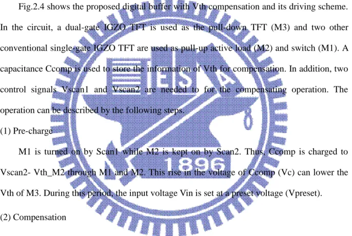
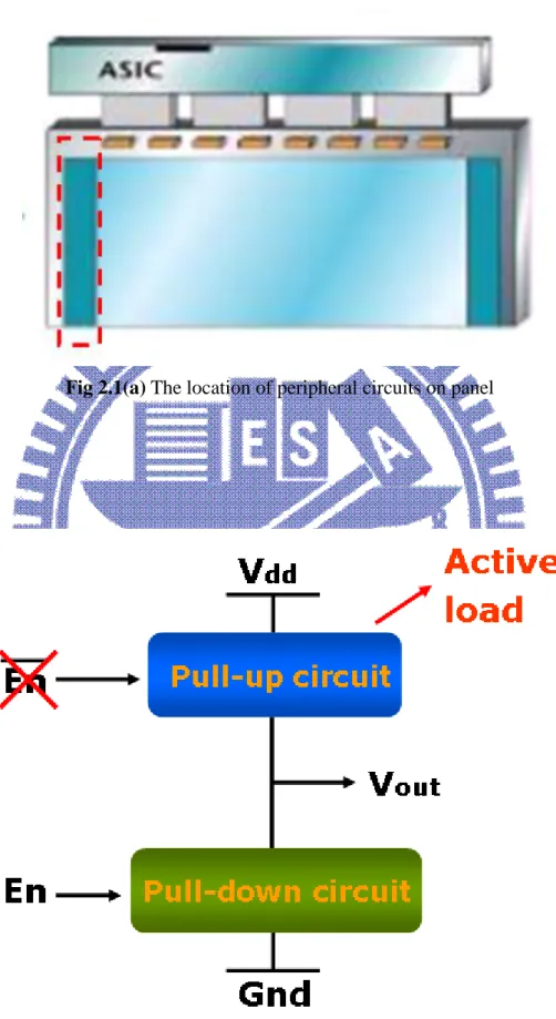
Fig 2.1(a) shows the location of the peripheral circuit on a display panel, where the the scan driver is integrated onto the display panel and marked by the red rectangle. The integrated scan driver can be represented by a simplified block structure, as shown in Fig 2.1(b). The lower and upper blocks are pull-down circuits and pull-up circuits and controlled by two lines EN and EN , respectively..
In many conventional circuits of NMOS [12, 13], the pull-up circuits are replaced by an active load. Some examples are shown in Fig. 2.2. As an active load, of pull-up transistor can tolerate more Vth variation. Therefore, the pull-down circuit is decisive for the function. Error probably occurs when Vth of the pull-down transistor shifts. In this chapter, a compensated mechanism is proposed to avoid the malfunction of this kind of integrated scan driver.
2.2 Vth Compensation
2.2.1 Reference Circuit
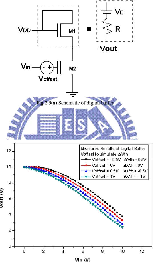
In this chapter, we use the simplest digital buffer to be the reference circuit to demonstrate the effectiveness of Vth compensation for peripheral circuits for driving. It is consisted of one active load (M1) and one pull-down transistor (M2) and shown in Fig 2.3(a).
Two conventional single-gate IGZO TFT are used to make the reference circuit. By adding a positive or negative DC voltage source (Voffset) between the input voltage Vin and gate of M2, we can imitate the Vth shifts negatively or positively for the same amount,
respectively.
Fig 2.3(b) shows the transfer curves of digital buffer with VDD at 10V for Voffset varying
from -0.5V to 1V, which imitates the Vth shift from 0.5V to -1V. The transfer function of the digital buffer is shifted by the variation of Vth accordingly. This variation of output level might be enlarged when the digital buffers are cascaded.
2.2.2 Proposed Circuit
Fig.2.4 shows the proposed digital buffer with Vth compensation and its driving scheme. In the circuit, a dual-gate IGZO TFT is used as the pull-down TFT (M3) and two other conventional single-gate IGZO TFT are used as pull-up active load (M2) and switch (M1). A capacitance Ccomp is used to store the information of Vth for compensation. In addition, two control signals Vscan1 and Vscan2 are needed to for the compensating operation. The operation can be described by the following steps.
(1) Pre-charge
M1 is turned on by Scan1 while M2 is kept on by Scan2. Thus, Ccomp is charged to Vscan2- Vth_M2 through M1 and M2. This rise in the voltage of Ccomp (Vc) can lower the Vth of M3. During this period, the input voltage Vin is set at a preset voltage (Vpreset). (2) Compensation
After the compensation step, Vscan1 turns off M1 and thus the information of Vth is stored in Ccomp. From the view point of bottom gate (BG) operation, Vth is fixed at constant. Thus, input voltage Vdrive fed to the bottom-gate of M3 can correspond to a fix output voltage.
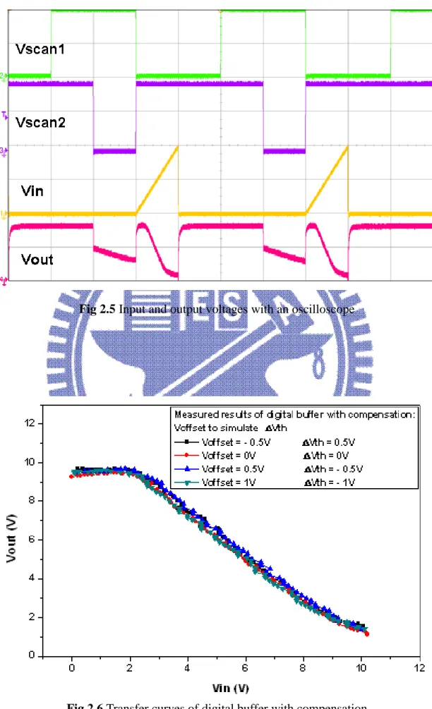
Because the compensation is a dynamic operation, the transfer curve of the proposed circuit cannot be obtained by the DC source-measurement unit. An alternative measurement method is used. The low and high voltages of both Vscan1 and Vscan2 are set at 0V and 10V, respectively. The preset voltage of Vin is set at 0V and changed to a sawtooth waveform from 0V to 10V in driving period. By simultaneously measuring the input and output voltages with an oscilloscope, as shown in Fig. 2.5, the transfer curve of the proposed circuit can be obtained by corresponding the input and output voltages in the time frame.
Similar to the measurement of the reference circuit, a DC voltage source (Voffset) is added to simulate the Vth variation of M3. The experimentally measured transfer curves of the proposed circuit for various Voffset are shown in Fig 2.6. Apparently, the transfer curves of the proposed digital buffer overlap owing to the compensation mechanism for the Vth variation.
2.3 Comparison
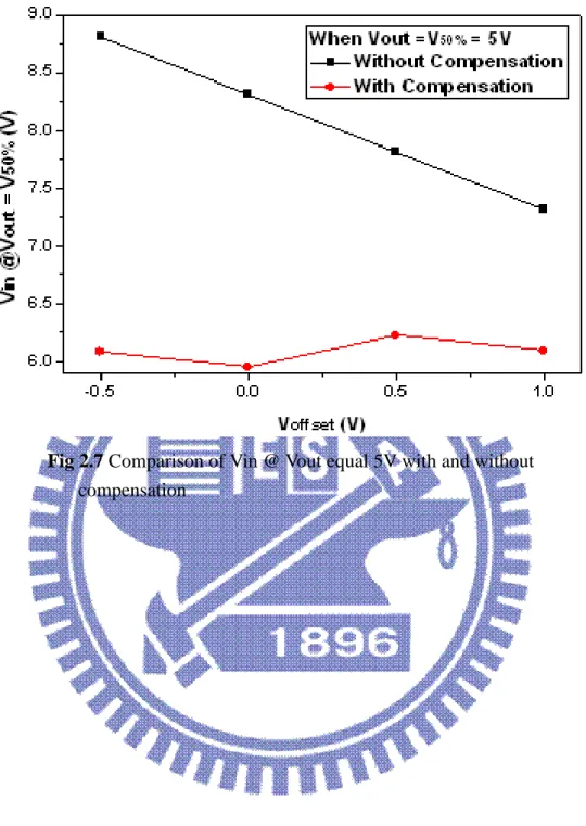
The effectiveness of the proposed compensation mechanism is apparent by comparing Fig 2.4 and 2.6. For quantitative comparison, an index extracted from the transfer curve is required. The index is chosen to be the input voltage Vin when Vout equals to VDD/2. As
shown in Fig 2.7, the variation of this Vin index without compensation is up to about 1.5V for Vth shift of 1.5V. As for the proposed digital buffer with compensation, the Vth variation of 1.5V only results in 0.37V difference. .
The better performance of the proposed circuit is further confirmed by another experiment. A dual-gate IGZO is used to build the pull-down transistor in the proposed circuits. This very transistor is also used to build the reference circuit with its top and bottom gates shorted
together. After measuring the transfer curves of the both circuits, the same transistor is subject to a voltage stress at the bottom gate of 10V for 90 seconds, which results in variation of Vth about 0.56V, as shown in Fig 2.8. The transfer curves of digital buffers with and without compensation before and after the device stress are compared in Fig. 2.9. The extracted index Vin when Vout equals 5V for proposed digital buffer varies only about 0.13V after the device stress, while for the simple digital buffer, it is up to about 0.48V.
2.4 Summary
We use the simplest digital buffer to experimentally demonstrate the concept of Vth compensation using dual gate IGZO TFTs. . The proposed method can compensate the Vth variation of pull-down transistor effectively. Even though this concept is only demonstrated in a simple circuit, the compensation method can be applied to other more complicated circuits.
Fig 2.1(a) The location of peripheral circuits on panel
Fig 2.3(a) Schematic of digital buffer
Fig 2.5 Input and output voltages with an oscilloscope
Fig 2.7 Comparison of Vin @ Vout equal 5V with and without compensation
-20 -10 0 10 20 1E-11 1E-10 1E-9 1E-8 1E-7 1E-6 1E-5 1E-4 1E-3 0.01 0.1 1 Id ( A ) Vbg (V)
Dual Gate IGZO measured @Vd=10V Initial: Vtg = 0V
Vtg = 10V
After M2 stressed 90(s) @Vbg = 10V: Vtg = 0V
Vtg = 10V
Fig 2.8 Id–Vbg transfer characteristics of the dual gate TFT before and after voltage stress
0 2 4 6 8 10 12 0 2 4 6 8 10 12 V o u t (V ) Vin (V)
Transfer Curve of Digital Buffer Without Compensation: Initial M2 Stressed 90 (s) @Vbg = 10V With Compensation: Initial M2 Stressed 90 (s) @Vbg = 10V
Fig 2.9 Transfer curve of simple and proposed digital buffer before and after voltage stress
Chapter 3
AMOLED Pixel Circuits
3.1 Types of OLED
Because of its high transparency and good conductivity, most reported OLEDs are the type of normal OLED, which are built on top of the ITO anode on the substrate[13]. In contrast to a normal OLED, an inverted OLED uses a bottom cathode connected to the drain end of an n-channel TFT [14]. Fig. 3.1 shows the structures of these devices respectively.
For the inverted OLED, large barrier exists between ITO and the electron transport layer (ETL), and thus results in poor electron injection characteristics and large operation voltage. However, the inverted OLED is more suitable to the pixel circuits with n-channel TFT because VGS of the driving TFT would not change after stress and the driving current of
OLED can keep constant.
Because normal and inverted OLEDs have their respective advantages and disadvantages, in this chapter, the proposed new concept of using the top-gate to compensate the Vth difference is applied in the AMOLED pixel circuits with both normal and inverted OLEDs.
3.2.1.1 Schematic and Operation
Fig. 3.2 shows the pixel circuit with inverted OLED and its driving scheme. In the circuit, a dual-gate IGZO TFT is used as the driving TFT (MD) and three other conventional single-gate IGZO TFT are used as switches. Two capacitors, namely, the storage capacitor Cst and the compensating capacitor Ccomp, are used to store the information of data voltage and Vth compensation, respectively. In addition, three control lines are needed to operate the pixel circuit. The operation of the pixel circuit is described in the following steps.
(0) Previous driving
For almost a frame time, M1 and M3 are off and M2 is on. The voltage stored in Cst sets the bottom-gate of MD and thus determines the current and the illumination of the OLED. (1) Pre-charge
Then, M1 is turned on by Vscan1 while M2 is kept on, so that Ccomp is charged to Vdd through M1 and M2. This rise in the voltage of Ccomp (Vc) can lower the Vth of MD. During this period, the data bus voltage (Vdata) is set at a preset voltage (Vpreset).
(2) Compensation
Before the real driving voltage (Vdrive) coming in, M3 is turned on by Vscan3 and Vdata is kept at the preset voltage for compensation. Meanwhile, M2 is switched to off by Vscan2 and M1 is kept on by Vscan1. In such a case, Vc is discharged through M1 and MD and thus raises the Vth of MD. This discharge current stops when Vc comes to a voltage that changes the Vth of MD to match the preset voltage at the bottom-gate to turn off the transistor. Therefore, the Vth of MD can be set at a predetermined value by the voltage at its top-gate. (3) Driving
After the compensation step, Vscan1 turns off M1 and thus the information of Vth is stored in Ccomp. Vdrive is fed to the bottom-gate of MD through M3, which is later turned off by Vscan3. Vdrive is stored in Cst to drive the OLED for a frame time.
3.2.1.2 Experimental Result
In the experiments, for simplification, Vdata is fed directly to the bottom-gate of MD instead of being driven through M3 and stored in Cst. The OLED is simulated by a 1M resistor and a 2.5V DC voltage source, corresponding to the turn-on resistance and cut-in voltage, accordingly. The low and high voltages for Vscan1 and Vscan2 are -5V and 15V, respectively. Furthermore, Vdata is modified to simulate the Vth variation from various devices. For example, the preset voltage Vpreset of 5V for compensation and driving voltage Vdrive of 8V are synchronously increased or decreased 0.5V to imitate that the Vth shifts negatively or positively for the same amount, accordingly.
The experimental result for 4T2C circuit is shown in Fig. 3.3. As can be seen, it is distinguishable in Vc that different sets of Vdata correspond to different discharge curves. For the lower Vdata input simulating the higher Vth, Vc is discharged to the higher value to compensate the Vth shift of MD. In such a case, the output voltage Voled converges to almost the same value. In other words, the compensation mechanism reduces the Vdata variation range of 1.5V to only about 0.11V difference in Voled, which verifies the circuit’s ability of Vth compensation.
Fig. 3.4 compares the experimental results for the circuit with and without Vth compensation. The case without compensation is measured by disconnecting M1 and Ccomp to exclude the effect of top-gate electrode. The variation of Voled owing to Vth shift of 1.5V is up
Cst and the compensating capacitor Ccomp, are used to store the information of data voltage and Vth compensation, respectively. In addition, four control lines are needed to operate the pixel circuit. The operation of the pixel circuit is described in the following steps.
(0) Previous driving
For almost a frame time, M1, M2 and M4 are off and M3 is on. The voltage stored in Cst sets the bottom-gate of MD and thus determines the current and the illumination of the OLED.
(1) Pre-charge
Then, M1 is turned on by Vscan1, M2 kept off and M3 is turned off by Vscan3, so that Ccomp is charged to Vscan1 –Vth_M1 through M1. This rise in the voltage of Ccomp (Vc) can lower the Vth of MD. During this period, the data bus voltage (Vdata) is set at a preset voltage (Vpreset).
(2) Compensation
Before the real driving voltage (Vdrive) coming in, M4 is turned on by Vscan4 and Vdata is kept at the preset voltage for compensation. Meanwhile, M1 is switched to off by Vscan1, M3 kept off and M2 is turned on. In such a case, Vc is discharged through M2 and MD and thus raises the Vth of MD. This discharge current stops when Vc comes to a voltage that changes the Vth of MD to match the preset voltage at the bottom-gate to turn off the transistor. Therefore, the Vth of MD can be set at a predetermined value by the voltage at its top-gate.
(3) Driving
After the compensation step, Vscan2 turns off M2 and M1 kept off, thus the information of Vth is stored in Ccomp. Vdrive is fed to the bottom-gate of MD through M4, which is later turned off by Vscan4. Vdrive is stored in Cst to drive the OLED for a frame time.
In the experiments, for simplification, Vdata is fed directly to the bottom-gate of MD instead of being driven through M4 and stored in Cst. The OLED is simulated by a 1M resistor and a 2.5V DC voltage source, corresponding to the turn-on resistance and cut-in voltage, accordingly. The low and high voltage for Vscan1 is 0V and 10V, then the low and high voltages for Vscan2 and Vscan3 are -5V and 15V respectively. Furthermore, Vdata is modified to simulate the Vth variation from various devices.
The experimental result for 5T2C circuit is shown in Fig. 3.6. As can be seen, it is distinguishable in Vc that different sets of Vdata correspond to different discharge curves. In such a case, the output voltage Voled converges to almost the close value. Namely, the compensation mechanism reduces the Vdata variation range of 1.5V to only about 0.67V difference in Voled, which verifies the circuit’s ability of Vth compensation.
Fig. 3.7 compares the experimental results for the circuit with and without Vth compensation. The case without compensation is measured by disconnecting M1, M2 and Ccomp to exclude the effect of top-gate electrode. The variation of Voled owing to Vth shift of 1.5V is up to about 2.77V. The performance of compensation is obvious in the proposed circuit.
3.3.1 4T2C circuit
3.3.1.1 Schematic and Operation
Fig. 3.8 shows the pixel circuit with normal OLED and its driving scheme. In the circuit, a dual-gate IGZO TFT is used as the driving TFT (MD) and three other conventional single-gate IGZO TFT are used as switches. Two capacitors, namely, the storage capacitor Cst and the compensating capacitor Ccomp, are used to store the information of data voltage and Vth compensation, respectively. In addition, three control lines are needed to operate the pixel circuit. The operation of the pixel circuit is described in the following steps.
(0) Previous driving
For almost a frame time, M1 and M3 are off and M2 is on. The voltage stored in Cst sets the bottom-gate of MD and thus determines the current and the illumination of the OLED. (1) Pre-charge
Then, M1 is turned on by Vscan1 while M2 is kept on, so that Ccomp is charged to Vdd through M1 and M2. This rise in the voltage of Ccomp (Vc) can lower the Vth of MD and thus increase the OLED current and illumination. However, during this period, the data bus voltage (Vdata) is set at a preset voltage (Vpreset), which is relatively low to avoid the high current of MD induced by the top-gate voltage (Vc) to minimize the unwanted illumination of the OLED.
(2) Compensation
Before the real driving voltage (Vdrive) coming in, M3 is turned on by Vscan3 and Vdata is kept at the preset voltage for compensation. Meanwhile, M2 is switched to off by Vscan2 and M1 is kept on by Vscan1. In such a case, Vc is discharged through M1 and MD and thus raises the Vth of MD. This discharge current stops when Vc comes to a voltage that changes the Vth of MD to match the preset voltage at the bottom-gate to turn off the transistor. Therefore, the Vth of MD can be set at a predetermined value by the voltage at its top-gate. (3) Driving
After the compensation step, Vscan1 turns off M1 and thus the information of Vth is stored in Ccomp. Vdrive is fed to the bottom-gate of MD through M3, which is later turned off by Vscan3. Vdrive is stored in Cst to drive the OLED for a frame time.
3.3.1.2 Experimental Result
In the experiments, for simplification, Vdata is fed directly to the bottom-gate of MD instead of being driven through M3 and stored in Cst. The OLED is simulated by a 1M resistor and a 1V DC voltage source, corresponding to the turn-on resistance and cut-in voltage, accordingly. The low and high voltages for Vscan1 and Vscan2 are -5V and 15V, respectively. Furthermore, Vdata is modified to simulate the Vth variation from various devices.
The experimental result for 4T2C circuit is shown in Fig. 3.9. As can be seen, it is distinguishable in Vc that different sets of Vdata correspond to different discharge curves. In such a case, the output voltage Voled converges to almost the same value. Namely, the compensation mechanism reduces the Vdata variation range of 1.5V to only about 0.1V difference in Voled, which verifies the circuit’s ability of Vth compensation.
Fig. 3.10 compares the experimental results for the circuit with and without Vth compensation. The case without compensation is measured by disconnecting M1 and Ccomp to exclude the effect of top-gate electrode. The variation of Voled owing to Vth shift of 1.5V is up to about 0.6V. The performance of compensation is obvious in the proposed circuit.
(a)
(b)
Fig 3.4 The experimental results for the 4T2C circuit using inverted OLED with and without Vth compensation
Fig 3.7 The experimental results for the 5T2C circuit with and without Vth compensation
Fig 3.10 The experimental results for the 4T2C circuit using normal OLED with and without Vth compensation
Chapter 4
Conclusion And Futrure Work
4.1 Conclusion
A new concept using the top-gate of the dual-gate IGZO TFT to compensate the Vth is proposed. The validity of the Vth compensation is verified in examples of digital buffer and AMOLED pixel circuits. The performance of compensation is apparent. Applying this concept, new circuits can be invented.
4.2 Future work
For the next step, we will try to improve or simplify the structure of Vth compensation circuits of AMOLED pixel to achieve higher aperture ratio and operation frequency. Furthermore, we will apply this Vth compensation concept to other circuits with the requirement of Vth compensation, such as active sensing pixel circuits, in the similar manner.
References
[1] Joon Chul Goh, Hoon Ju Chung, Jin Jang, and Chul Hi Han, “A New Pixel Circuit for Active Matrix Organic Light Emitting Diodes”, IEEE Electron Device Lett, VOL. 23, pp. 544-546, NO. 9, SEPTEMBER 2002
[2] Roger G. Stewart, “Active Matrix OLED Pixel Design”, SID Symposium Digest of Technical Papers, May 2010, Volume 41, Issue 1, pp. 790-793
[3] Jae Hoon Lee, Ji Hoon Kim, and Min Koo Han, “A New a-Si:H TFT Pixel Circuit Compensating the Threshold Voltage Shift of a-Si:H TFT and OLED for Active Matrix OLED”, IEEE ELECTRON DEVICE LETTERS, VOL. 26, p.897-899, NO. 12, DECEMBER 2005
[4] Young Ju Park*, Myoung Hoon Jung, Sang Ho Park, and Ohyun Kim, “Voltage-Programming-Based Pixel Circuit to Compensate for Threshold Voltage and Mobility Using Natural Capacitance of Organic Light-Emitting Diode”, Japanese Journal of Applied Physics 49 (2010) 03CD01
[5] Seung Min Lee, Chang Il Ryoo, Jae Wook Park, “Control of Threshold Voltage in Back Channel Etch Type Amorphous Indium Gallium Zinc Oxide Thin Film Transistors”, SID Symposium Digest of Technical Papers, May 2011, Volume 42, Issue 1, pp. 104-106 [6] Byung Seong Bae, Jae Won Choi, Jae Hwan Oh, and Jin Jang, “Level Shifter Embedded
219-221, Mar. 2010
[9] Kyoung Seok Son, Ji Sim Jung, Kwang Hee Lee, “Highly Stable Double-Gate Ga–In–Zn–O Thin-Film Transistor”, IEEE ELECTRON DEVICE LETTERS, VOL. 31, pp.812-814, NO. 8, AUGUST 2010
[10] Semiconductor Devices: Physics and Technology” by S. M. Sze, p. 213
[11] Peyman Servati, Karim S. Karim, Arokia Nathan, “Static Characteristics of a-Si:H Dual-Gate TFTs”, IEEE Trans. on Electron Devices, vol. 50, no. 4, pp. 926-932, Apr. 2003
[12] Binn Kim, Seung Chan Choi, Seung Hee Kuk, “A Novel Level Shifter Employing IGZO TFT”, IEEE Electron Device Letters , VOL. 32, p.167-169, NO. 2, FEBRUARY 2011 [13] Mallory Mativenga, Min Hyuk Choi, Jae Won Choi, “Transparent Flexible Circuits
Based on Amorphous-Indium–Gallium–Zinc–Oxide Thin-Film Transistors”, IEEE ELECTRON DEVICE LETTERS, VOL. 32, p.170-172, NO. 2, FEBRUARY 2011 [14] Ching W. Tang, and Steven Van Slyke, “Organic electroluminescent diodes”, Applied
Physics Letters, Volume 51, Issue 12, p.913-915,Sep 1987.
[15] Hsing Hung Hsieh, Tsung Ting Tsai, Chin Yu Chang, “A 2.4-in. AMOLED with IGZO TFTs and Inverted OLED Devices”, SID Symposium Digest of Technical Papers, May 2010, Volume 41, Issue 1, pp. 140-143