國
立
交
通
大
學
電機學院光電顯示科技產業研發班
碩
士
論
文
四點探針有機薄膜電晶體之氣體感測研究
Study of Gas Sensing Ability on Gated-Four-Probes
Organic Thin Film Transistors
研 究 生:吳文馨
指導教授:冉曉雯 博士
四點探針有機薄膜電晶體之氣體感測研究
Study of Gas Sensing Ability on Gated-Four-Probes
Organic Thin Film Transistors
研 究 生:吳文馨 Student:Wen-xin Wu
指導教授:冉曉雯 Advisor:Dr. Hsiao Wen Zan
國 立 交 通 大 學
電機學院光電顯示科技產業研發碩士班
碩 士 論 文
A Thesis
Submitted to College of Electrical and Computer Engineering National Chiao Tung University
in partial Fulfillment of the Requirements for the Degree of
Master in
Industrial Technology R & D Master Program on Photonics and Display Technologies
August 2007
Hsinchu, Taiwan, Republic of China
四點探針有機薄膜電晶體之氣體感測研究
研究生:吳 文 馨 指導教授:冉曉雯 博士
國立交通大學
電機學院光電顯示科技產業研發碩士專班
摘
要
在論文中,我們建立一個可定量控制氣體濃度的感測系統,並利用具四 點探針結構的有機薄膜電晶體進行氨氣感測的研究。當氨氣與有機薄膜電晶體反 應時,電晶體的汲極電流會被減少、臨界電壓會往負值增加、但次臨界擺幅幾乎 不受氨氣的影響而改變。而由四點探針結構的量測顯示,電晶體的薄膜電阻與接 觸電阻均隨氨氣濃度的提高而增加。而利用薄膜電阻所推算出來的本質載子遷移 率也會因氨氣濃度的提高而隨之減少。最後則將探討載子遷移率降低、臨界電壓 往負值增加、及幾乎不受氨氣影響的次臨界擺幅,並根據電晶體特性改變的結 果,提出可能的反應機制。
Gas sensing ability of Gated-Four-Probes OTFTs study
Student: Wen-xin Wu Advisor: Dr. Hsiao-Wen Zan
Industrial Technology R & D Master Program of
Electrical and Computer Engineering College
National Chiao Tung University
Abstract
In this thesis, we tried to construct a gas sensing system, in which we can
control the gas concentration quantitatively; moreover we also utilized the
gated-four-probes organic thin film transistor to investigate the NH3 gas-sensing
experiment. When the NH3 gas was interacted with OTFT, it was found that
the OTFT drain current will be reduced and the threshold voltage will be
enlarged toward a negative value. However, the subthreshold swing was not
changed significantly by the NH3 gas. From the analysis of gated-4-probes
OTFT, both the film resistance and the contact resistance were increased with
the raise of NH3 concentration. Additionally, the intrinsic field-effect mobility,
which was estimated from the film resistance, was also reduced with the raise of
threshold voltage, and the almost unchanged subthreshold swing were discussed.
A probable mechanism deduced from the change of the OTFT was also
summarized and proposed in this study.
Acknowledgement
在這兩年的碩士班生涯期間,首先要感謝的是指導教授冉曉雯老師,老師在 我的碩士班研究題目上給我的建議,和對於這個主題的未來展望,您悉心的教導 使我得以一窺有機薄膜電晶體領域的深奧,不時的討論並指點我正確的方向,使 我在這兩年中獲益匪淺。 本論文的完成另外亦得感謝生化工程研究所的楊裕雄教授在硬體上大力支 持,及生化工程研究所羅淵仁和蕭程允學長的協助,提供我實驗上所需要的設 備。因為有你們的體諒及幫忙,使得本論文能夠更完整而嚴謹。 感謝實驗室的學長們,在我對於研究上的一些疑惑,和你們討論後總是能激 發我一些靈感,啟發我再去思考的動力。特別感謝國錫學長,總是不厭其煩的指 出我研究中的缺失,並給予建議。也感謝實驗室的同學們:芸嘉、廷遠、高手、 小七、睿志、光明、而康同學的幫忙,恭喜我們順利走過這兩年。實驗室的武衛、 權陵、俊傑、志宇學弟、旻君學妹,你們幫忙我銘感在心。 最後,謝謝我的家人,感謝你們從小到大的支持與照顧! 吳文馨 2007 夏 于新竹Contents
Chinese Abstract ……… i
English Abstract ……… ii
Acknowledgment ……… iv
Contents ……… v
Figure Captions ……… vii
Chapter 1 Introduction……… 1
1-1 Introduction of organic thin film transistors (OTFTs) ….…... 1
1-2 Applications of OTFTs to gas-sensing device………... 2
1-3 Objective and Motivation………... 2
1-4 Organization of thesis……….………. 3
Chapter 2 Theoretical background of OTFTs………...… 5
2-1 Transportation mechanisms of organic semiconductor……... 5
2-2 Interaction of gases on OTFTs………….……… 7
2-3 Potential Effects on Gas Sensing in OTFT……….……. 8
2-3.1 Morphology and dimension of Active Layer…….………….. 8
2-3.2 Dipole of the analyte……….………... 9
2-3.3 The Thickness of Active Layer……….………... 9
2-4 Gated four-probes OTFTs for resistance measurement……... 10
CHAPTER 3 EXPERIMENT……….. 13
3-1 Device Fabrication…….……….. 13
3-1.1 Preparation of Substrates……….……… 13
3-1.2 Spin-coated PMMA on SiO2……….………... 13
3-1.3 Growth of Thin Film and Electrodes……….………….. 14
3-2 Gas sensing system………...……….………….. 14
CHAPTER 4 Result and Discussion……….………..………. 16
4-1 Characteristics of Gated-Four-Probes OTFTs…….………… 16
4-2 Effects of ammonia (NH3 ) on Gated four-probe OTFTs….... 18
CHAPTER 5 Conclusion...……….………..………. 23
Figure Captions
Chapter 1
Figure 1.1 The applications of plastic transistors: (a) flexible displays, (b) smart cards, (c) RFID tags, and (d) the nervous system of robot skin. Figure 1.2 Evolution of hole mobility for the most common p-type organic
semiconductors. Chapter 2
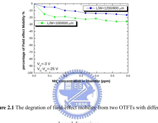
Figure 2.1 The degration of field-effect mobility from two OTFTs with different channel dimensions.
Figure 2.2 (a) Top view of a gated-four-probes OTFT. (b) The potential distribution in an OTFT channel region. The potential drop of the organic film is assumed to be linear. But the potential different at the source and drain electrodes are also given.
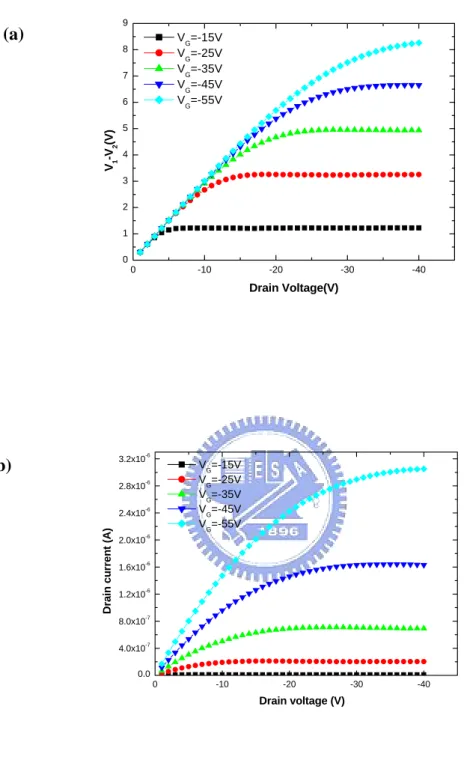
Figure 2.3 The voltage difference between two voltage probes V1− are plotted V2
as a function of drain voltage at different gate voltage. Chapter 3
Figure 3.1 Diagram of gas sensing measurement system
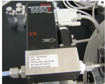
Figure 3.2 The mass flow controller of gas sensing system. (b) The power supply of mass flow controller. (c) The pressure gauge of gas sensing system. Figure 3.3 Top-view image of gas-sensing system.
Figure 3.4 Top-view image of gas-sensing system mounting a metal cap with transparent window.
Chapter 4
Figure 4.1 The atomic force microscope (AFM) images of (a) SiO2 dielectric. (b)
PMMA-coated SiO2 dielectric. (c) pentacene AFM image on
PMMA-coated SiO2 layer.
Figure 4.1 The drain-current is plotted as a function of gate-voltage. (a) Device is operated at linear region. (b) Device is operated at saturation region. Figure 4.3 (a) The voltage difference between potential-probes is plotted as a
function of drain voltage, at different gate voltagde respectively. (b) The output characteristics (ID−VD ) show that when V increases, the D
D D
I −V curve will be converted from a linear-relation to a saturated-relation.
Figure 4.4 The transfer characteristic of gate-four-probes OTFT is plotted in (a) semi-log scale and (b) linear-scale, respectively.
Figure 4.5 The total contact resistance(Rcont) and the pentacene film resistance (Rfilm) is plotted as a function of gate-voltage minus threshold-voltage (VG−Vth), respectively.
Figure 4.6
(a) The Rcont and Rfilm is further plotted as a function of NH3
concentration. (b) The percentage (%) of Rcont and Rfilm versus NH3
concentration.
Figure 4.7 4-7 The extracted ontrinsic field-effect mobility is plotted as a function of NH3 concentration gas at a VD = −3V and VG−Vth = −25V .
Figure 4.8 4-8 (a) The threshold voltage shift (Δ ) and (b) the subthreshold swing Vth
(S S. .) is also plotted as a function of NH3 concentration, respectively.
Figure 4.9 4-9 The estimated GB barrier height and GB trap density is plotted as a function of NH3 concentration.
Figure 4.10 4-10 The subthreshold swing and interface trap density will not be influenced significantly after the pentacene film interacts with the NH3
CHAPTER 1
Introduction
1.1
Introduction of organic thin film transistors (OTFTs)
“Plastic transistors” open the future of flexible displays, smart cards, radio
frequency (RF) identification tags, as well as light-emitting diodes (LED) and lasers
[1]. Rapid progress in this field has been achieved by improving the material
properties and the process techniques .
As for the application of electronics, the organic active layer has attended a
mobility of 1cm2/Vs and a switching speed of 108 Hz, which is comparable to
amorphous hydrogenated silicon (a-Si:H) , as shown in Fig. 2.1 [2]. Since the late
1940s, there has been a lot of research on the development of organic semiconductor
[3]. This is because of the large π-conjugation length along the long axis of the
molecules and closed π-stacking are the key factors of high carrier mobility [3].
Similar to inorganic semiconductors, organic ones can function as p-type or
n-type. However, most reported high-mobility organic semiconductors are p-type
material. Among the p-type material, pentacene (C14H22), a rod-like aromatic
molecule composed of five benzene rings, shows the highest mobility (>1cm2/Vs),
owning to highly ordered films with proper dielectric properties and growth
1.2
Applications of OTFTs to gas-sensing device
For the next generation of sensor applications on medical diagnostics, food
monitoring, and chemical or biological warfare etc.; portable, low cost, and low
power-consumption will be important demands. As for these demands, the OTFT
should be an important candidate due to its flexibility and its simple fabrication
process. Therefore, the studies of organic thin-film transistors (OTFTs) to physical,
chemical, and biological sensors will become an important object [5,6,7,8].
Recently, OTFTs are proposed to act as gas sensors. When OTFTs exposed to
gaseous species, five parameters: such as the turn-on current (Ion), turn-off current
(Ioff ), threshold-voltage (Vth), field-effect mobility (μ ) and subthreshold-swing eff
( ), are used to estimate the gaseous interaction in OTFTs. By this way, a
“multi-parameter” gas sensor can be realized by OTFT [9].
. .
S S
1.3
Objective and Motivation
Although the primary gaseous interactions on OTFTs are observed, however, the
details of mechanisms are still not well-understood. Unlike the inorganic materials,
the bindings between the organic molecules are weak van der Waal force. The stack
of organic crystal is loose and contained with voids. Therefore, the gas penetration
semiconductor layer. Besides, the loosely packed organic-film with aromatic
compounds will be a good medium for bio-molecules. As a result, to investigate the
fundamental of gaseous and biochemical interaction on OTFTs should open a road to
high-sensitive organic sensors.
In this study, we try to investigate the effect of sensing ammonia(NH3) in
pentacene-based OTFTs. By the gated-4-probes OTFTs, the organic film properties
and mental-contact effects can be studied separately. The related parameters of TFT,
such as pentacene film resistances, intrinsic mobility, threshold voltage, and the
subthreshold swing, will also be monitored during the gaseous experiment on OTFTs.
Afterwards, we will try to analyze these parameters to characterize the sensing
mechanism and propose a potential model.
1.4
Organization of thesis
In chapter 1, we make a brief introduction to the demands on OTFTs and its
application on gas sensing. Consequently, in chapter 2, we discuss some basic
knowledge about the device operations and the gas sensing properties in OTFTs.
The studies of gated-4-probes OTFTs and its analysis are also presented in this part.
In chapter 3, the experimental details, such as the devices fabrication, and the
connection of gas sensing system are discussed. The effect of sensing ammonia(NH3)
these chapters. The related OTFT parameters will also analyze under different gas
CHAPTER 2
Theoretical background of OTFTs
2-1 Transportation mechanisms of organic semiconductor
In the past 20 years, a great deal of progress has been made in improving the field-effect mobilities of OFETs [10,11]. It has also been demonstrated that the
properties of charge transport in conjugated molecules are intrinsically correlated with
their crystalline structure, where the π delocalized carriers are responsible for the
intra-molecular conduction.However, the nature of van der Waals bonding between
discreted molecules is thought to be a limitation of the carrier transport, and the
transport is usually described by “localized model” [3]. Thus, the charged carrier
transport must be described by different models than those in covalently bonded
semiconductors.
Recently, two principal types of theoretical models are used to describe the
transport in organic semiconductors : “The band-transport model” and “The hopping
models”. However, band transport may not suit for some disordered organic
semiconductors, in which carrier transport is govern by the hopping between localized
states. Hopping is assisted by phonons and the mobility increases with temperature.
Typically, the mobility is very low, usually much lower than 1cm2/V-sec. The
(~1cm2/V-sec) at room-temperature (RT) [12]. Many kinds of polycrystalline
organic semiconductors, such as several members of the acene series including
pentacene, rubrene, have RT mobility over the boundary [13]. Sometimes,
temperature-independent mobility was found in some polycrystalline pentacene
devices [14]. Thus, this observation argued that the simply thermal activated
hopping process governed the whole carrier transport behaviors in high quality
polycrystalline pentacene film, despite that the temperature independent mobility has
been observed in exceptional cases [14].
The understanding of carrier transport in single-crystal of organic
semiconductors will help us to describe the transport mechanism in polycrystalline
organic semiconductors. The coherent band-like transport of delocalized carriers
becomes the prevalent transport-mechanism in the single crystal organic
semiconductors, such as pentacene, tetracene, under the low-temperature
environments. A very high hole mobility has been measured by time-of-flight (TOF)
experiments [15]. Thus, the temperature dependence of the carrier mobility was
found below 100K and following with a power law of μ∝ T-n, n~1 [16], in single
crystals of organic semiconductors, consistent with the band-transport model.
However, between 100K and 300K, the carrier mobility show a constant value [16],
mechanisms. The first mechanism was small molecular polaron (MP). According
to this model, the carriers were treated as the heavy, polaron-type, and quasi-particles.
It is formed by the interaction of the carriers with intra-molecular vibrations of the
local lattice environment, and move coherently via tunneling. In this model, the
mobility follows the power law μMP=aT-n. The other involves a small lattice polaron
(LP), which moves by thermally activated hopping and exhibits a typical exponential
dependence of mobility on temperature :
μ
LP=bexp[-Ea/kT]. The superposition ofthese two mechanisms could get a good consistence with experimental measurement
of temperature-dependence mobility from room temperature to a Kelvin degrees (K)
[17].
2-2 Interaction of gases on OTFTs
The OTFTs gas sensing have been several advantages over the chemical resisters. These devices are especially attracted due to their ability to serve as a multi-parameter sensor [9].
Furthermore, Frank Liao indicated that there is the potential for discrimination
based on the functional group chemistry of the analytics. The presence of π orbitals
or the acidic proton in the acetic acid interacts with the channel of the device to cause
2-3 Potential Effects on Gas Sensing in OTFT
2-3.1 Morphology and dimension of Active Layer
Grain boundaries (GBs) play a critical role in OFET sensing. In the repored
researches, the control of grain size can be achiered by changing the substrate temperature during deposition. According to the images of transmission electron
microscope (TEM), Torsi et al. indicate that the response is strong for the
low-temperature film, which has more grain boundaries. However, the response is
weak for the high-temperature film, which has fewer grain boundaries and shows a
more compacted structure [18].
Wang et al. also indicate that device channel scale being an important key in
sensing process with different mechanisms dominating at different length scales. For a
longer channel relative to grain sizes, there are enough grain boundaries inside the
channel so that the former effect is dominant and the overall sensing response is the
current decreasing. For a shorter channel relative to grain sizes, the latter effect
dominates due to very few number of grain boundaries inside channel, which leads to
the current increasing by excess charges from the interaction between grains and the
2-3.2 Dipole of the analyte
For the most analytes, the interactions are attributed to the nature of molecular
dipole. For example, the H2O will result in the decrease of drain-current
[20,21].Although pentacene is highly hydrophobic, H2O molecules can easily diffuse
into these devices, interact with the traps by and alter the electric field at the grain
boundaries. In addition, the presence of polarized molecules is known to decrease the
rate of charge transport in organic materials by increasing the amount of energetic
disorder through charge–dipole interactions [20].
2-3.3 The Thickness of Active Layer
Yang et al. indicate that ultrathin cobalt phthalocyanine(CoPc) transistors of 4
ML compare faster response times, higher base line stabilities, and more sensitive to
50 ML devices [22]. Due to the ultrathin ChemFETs, the holes accumulation extends
to the air/CoPc interface; therefore, the surface traps participate in carrier transport
and the perturbation of the surface trap energies by the analytes renders the ultrathin
ChemFETs more sensitive than the thick ChemFETs [22].
2-3.4 Device area
response. Different device areas of (W/L)1 = 500/25 and (W/L)2 = 100/4 both show
the same percent change in active current [7].
But in our gas sensing experiments from different dimension of OTFT are show
in Fig. 2.1. Different size OTFT will show a slightly different response.
2-4 Gated four-probes OTFTs for resistance measurement
Gated four-probe OTFTs measurements were carried out by using a Keithley
4200-SCS semiconductor parameter analyzer.In the four-terminal measurements,as
show in Fig. 2-2(a) the voltage and between the source and drain electrodes.
The probing current of voltage probes is about 10
1
V V2
-13A,which is lower than the
drain-current. In Fig. 2-2(b), an idealized depiction of the potential distribution in the
channel region, when OTFT is operated in linear region and above threshold condition VDS < VGS−VT . Where is the threshold voltage, is the
gate-source voltage, and
T
V VGS
DS
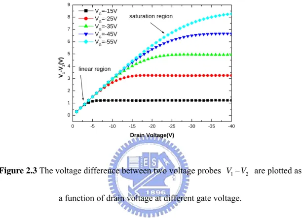
V is the drain-source voltage. In Fig. 2-3, the voltage
difference between the voltage probes V1− from four-terminal measurement. This V2
voltage difference varies linearly with increasing VDS over a limited range of VDS
and shows almost no gate voltage dependence. Such linear dependence on VDS is
expected if the device behaves as predicted by simple FET theory. At a large VDS, the
DS
V . This behavior is also predicted from simple FET theory for the saturation region.
By measuring, and , a linear extrapolation of the potential profile to each
contact was performed. The potential drops at the source electrode (ΔV
1
V V2
S)、drain
electrode (ΔVD) and organic film (ΔVFilm), were calculated according to the following
equations: 1 2 2 2 1 ( ) ( ) ( ) S V V V V L L V L L ⎡ − ⎤ Δ =⎢ − − − − ⎣ 2 ⎦⎥ S (1) 1 2 2 2 1 ( ) ( ) D D V V V V V L L L ⎡ − ⎤ Δ = −⎢ + − ⎣ 2⎦⎥ (2) 1 2 2 1 ( ) ( ) Film V V V L L − Δ = − L (3)
where VS, VD, , and are the voltages at the source, drain, and two potential
probes, respectively. is drain electrode to the first potential probe. is drain
electrode to the second potential probe. L is the distances from the drain electrode to
source electrode. Where is the actual voltage drop across the film.
1 V V2 1 L L2 Film V Δ
With the measured total current flowing through the device and the potential
drops across the film and contacts, the resistance of the source contact, drain contact,
and the film can be calculated using Ohm’s Law, when devices operation in linear
region. S S D V R I Δ = (4) D D D V R I Δ = (5)
F F D V R I Δ = (6)
CHAPTER 3
EXPERIMENT
3.1 Device Fabrication
3.1-1 Preparation of Substrates
In this study, the OTFT devices we used are top-contact structures. A p-type,
single crystal silicon wafer (100) was used as the substrate and the gate electrode.
After RCA cleaning, a 1000Å thermally-grown SiO2 layer was deposited on wafer by
furnace. After the SiO2 deposition, we removed the SiO2 layer from the wafer of
unpolished-side. The etching-solution we used is buffered oxide etching (B.O.E.)
solution (NH4F:HF=6:1). Hence, the wafer of unpolished-side without SiO2 layer
can serve as a gate-electrode. Finally, the substrate was cleaned in ultrasonic tank by
the sequence of: de-ionic water (5 minutes), acetone (1 minutes), and de-ionic water
(5 minutes).
3.1-2 Spin-coated PMMA on SiO
2After substrate cleaning, we spun the solution-based Polymethylmethacrylate
(PMMA) unto the substrate. The content of solution-based PMMA is a mix of
Consequently, we try to remove the residual solvent, by baking the substrate on
hot-plate at 90℃ about 30 minutes.
3.1-3 Growth of Thin Film and Electrodes
Pentacene powder was purchased from SIGMA-ALDRICH. Without any
purification, pentacene powder was sublimated and deposited on substrate as an active
layer under a pressure below 1.5×10⁻⁶ torr. The substrate was kept at 26℃. The
deposition rate was about 0.5Å/s and the pentacene-film thickness was about 1000 Å.
All the deposition parameters are monitored by a quartz crystal microbalance (QCM)
during the deposition process. In the end, a 1000Å Au layer was used as the source
and drain pad, which is deposited at a rate of 1~2 Å/sec under 3×10⁻⁶ torr. The
channel width (W) and length (L) defined by shadow-mask was 800μm and 1200μm,
respectively.
3.2 Gas-Sensing system
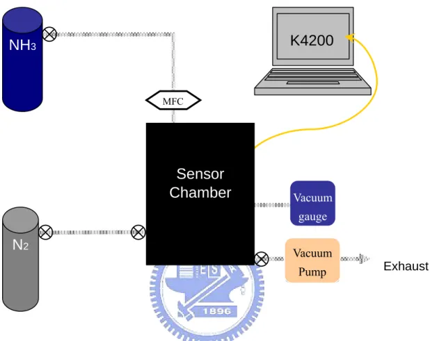
As shown in Fig. 3.1, the gas-sensing system consists of three major parts: a
gaseous analyte controller, a gas-proof chamber, and a semiconductor parameter
analyzer. In Fig. 3.2(a), (b), and (c), we show the mass flow controller, the power
the gas-proof chamber and controlled by the mass flow controllers (MFC; 5850E,
Brooks Instrument). The pressure inside the gas-proof chamber was monitored by
vacuum gauge (PC-615, PROTEC). The total volume of the gas-proof chamber is
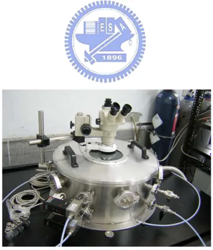
about 52.8 liter. Fig. 3.3 is the top-view image of gas-sensing system. The system
was equipped with five Kelvin-probes and positioners. The probes were connected
to the semiconductor analyzer (Keithley 4200-SCS) via tri-axial cables. The bottom
pipe and the upper pipe served as the gas-inlet and gas-exhaust, respectively. After
mounting a metal cap with transparent window, as shown in Fig. 3.4, the gas-proof
chamber can be pumped down to less than 1 torr. Consequently, we introduced the
pure nitrogen (N2) gas into the gas-proof chamber. Thus, all the gaseous-sensing
experiments can be processed in a low-humidity and low-oxygen ambiance. All the
CHAPTER 4
Result and Discussion
4-1 Characteristics of Gated-Four-Probes OTFTs
In order to improve the OTFTs performance and pentacene crystallization, the SiO2
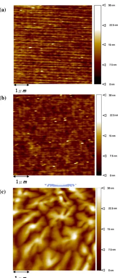
surface is spin-coated with an ultra-thin PMMA layer. In Fig. 4-1(a) and (b), we
show the atomic force microscope (AFM) images of SiO2 dielectric and
PMMA-coated SiO2 dielectric. As we can observe, the surface roughness of SiO2
and PMMA-coated SiO2 is about 0.21 nm and 0.20 nm, respectively. The PMMA
layer will not affect the surface roughness significantly. From the capacitance
measurements, the total capacitance value is reduced from 34 nF/cm2 to 23.4 nF/cm2
.
By the serious-capacitance formula:
2
1 1 1
total SiO PMMA
C =C +C 0 i i i C t ε ε⋅ = total C , , and 2 SiO
C CPMMA is the total capacitance, the SiO2 capacitance, and the
PMMA capacitance, respectively. εi is the permittivity in vacuum. εi and indicates the relative dielectric constant and the dielectric thickness, respectively. By taking the
i
t
2 3.9
SiO
ε = , tSiO2 =100nm, and εPMMA =3.5, the estimated thickness of
layer is also show in Fig. 4-1(c), an average grain-size and roughness about 1~2 μm
and 15.1 nm can be observed in the figure, respectively. After the source, drain, and
voltage-probing electrodes are deposited on pentacene film, we measured the transfer
characteristics of the gated-4-probes OTFT. The drain-current is plotted as a
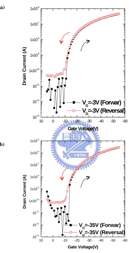
function of gate-voltage in Fig. 4-2. The devices shows an on/off current ratio about
5 order and a low hysteresis when the devices is operated above the threshold voltage.
To obtain correct parameters from gated-4-probes OTFT, it is important to choose
the range of operation voltage. It is well known that four-terminal electrical
measurement is based on the Ohm’s Law. The voltage-drop will be linearly changed
with the increase of drain-voltage. However, the linear-dependence is not always
expected at any voltage bias. As show in Fig. 4-3 (a), the voltage difference between
potential-probes is plotted as a function of drain voltage, respectively. The voltage
difference (V2−V1), will not linearly increase with drain-voltage (VD) and show
almost no gate-voltage (VG) dependence when the VD is less than –4 V. The result
can be explained by the output characteristics (ID−VD) in Fig. 4-3(b). When the
D
V increases, the ID−VD curve is converted from a linear-relation to a
saturated-relation. It is clear that when the gated-4-probes OTFT is operated at a
small VD e.g. less than -5 V, the extracted parameters will be correct. Hence, in the
4-2 Effects of ammonia (NH
3) on Gated four-probe OTFTs
Before the measurement, the gas-sensing chamber is pumped-down to less than 1
torr and vented to 760 torr by the high-purity nitrogen (N2) gas. Initially, we
measured the gated-4-probe OTFT in the nitrogen ambiance. As shown in Fig. 4-4(a)
and 4-4(b), the transfer characteristic is plotted in semi-log scale and linear-scale.
Under the nitrogen ambiance, the device show a mobility about 0.37 cm2
/V-sec, an
on/off current ratio more than 5 orders, a threshold voltage about -24 V, and a
subthreshold swing about 0.97 decade/V. When the NH3 is introduced into the
chamber, the drain-current ( ID ) will reduced with the increase of the NH3
concentration. Interestingly, the threshold voltage will also shift more negatively.
The on/off current ratio and the subthreshold swing will not be changed significantly
with the increase of the NH3 concentration.
To further study the effects of NH3 gas on OTFT devices, we try to estimate the
contact resistance and pentacene resistance by the gated-4-probe OTFT, respectively.
From potential-probes on channel, the voltage-drops at the source electrode ( ),
drain electrode ( S V Δ D V
Δ ), and within the pentacene film (ΔVfilm) can be estimated by:
1 2 2 2 2 1 ( ) ( ) ( ) S S V V V V L L V L L ⎡ − ⎤ Δ =⎢ − − ⎥− − ⎣ ⎦
1 2 2 2 2 1 ( ) ( ) D D V V V V V L L L ⎡ − ⎤ Δ = −⎢ + ⎥ − ⎣ ⎦ 1 2 2 1 ( ) ( ) Film V V V L L L − Δ = − 1
V and is the voltage measured from the first potential probe (near the drain
electrode) and second potential probe (near the source electrode), respectively.
and is the distance from the first potential probe to drain electrode and the second
potential probe to source electrode. is the channel length.
2 V 1 L 2 L L VD and is the
drain voltage and source voltage, respectively. The total contact resistance (
S
V
cont
R )
and film resistance (Rfilm) can also be estimate by:
S D cont D V V R I Δ + Δ = film film D V R I Δ =
As shown in Fig. 4-5, the Rcont and the Rfilm is plotted as a function of gate-voltage
minus threshold-voltage (VG−Vth), respectively. When the NH3 gas is introduce into
the gas-sensing chamber, both the Rcont and the Rfilm will increase. The Rcont
and Rfilm is further plotted as a function of injected NH3 in Fig 4-6(a). When the
injected NH3 is increased to 0.59 ppm, the Rcont will approach a maximum value
about 1.0×10⁶ Ω, which is smaller than the value of Rfilm around 8.3×10
6 Ω. The
Fig. 4-6(b) shows the percentage (%) of Rcont and Rfilm versus injected NH3,
during the NH3 gaseous experiment. Thus, the OTFT characteristics should be
mainly dominated by the pentacene film properties rather than the contact properties.
Since the pentacene film properties will dominate the OTFT characteristics during
the NH3 gaseous experiment, we try to observe the intrinsic variation of field-effect
mobility. In gated-4-probes measurement, the contact-corrected field-effect mobility (μ ) can be extracted by eff
1 eff total G C V σ μ = ⋅ ∂ ∂ 2 1 ' D I L V V W σ = ⋅ −
where Ctotal is the total capacitance of OTFT, σ is the conductivity, and is the voltage measured from the first potential probe (near the drain electrode) and
second potential probe (near the source electrode), is the distance between two
potential probes, and W is the channel width. The extracted contact-corrected
field-effect mobility is plotted as a function of injected NH
1
V V2
'
L
3 gas at a and
in Fig. 4-7. When the NH
3
D
V = − V
25
G th
V −V = − V 3 concentration is increased, the
contact-corrected field-effect mobility will decrease monochromatically from 0.39
cm2/V-sec to 0.34 cm2/V-sec. The threshold voltage shift (Δ ) and the subthreshold Vth
swing (S S. .) is also plotted as a function of NH3 concentration in Fig. 4-8(a) and Fig.
4-8(b), respectively. The threshold voltage will shift toward more negatively with
averaged value around 0.94±0.03 V/decade and seems not be effected by the NH3
dramatically, even when the NH3 concentration is approached to a concentration of
0.59 ppm.
In none-crystalline semiconductor, the carrier field-effect mobility will be
influenced by the grain-boundary (GB) potential barrier height qφb. The mostly
proposed GB barrier height model is described by
exp( b) eff ig q kT φ μ =μ ⋅ − 2 8 ( t b ) s ox G th qN d C V V φ ε = −
Where μ is intra-grain carrier mobility, q is elementary electron, ig is the
grain-boundary trap density, is the thickness of semiconductor,
t
N
d εS is the
semiconductor dielectric constant, is the gate insulator capacitance, is the
Boltzmann’s constant, and T is the absolute temperature. According to the
equation, the estimated GB barrier height and trap density is plotted as a function of
NH
ox
C k
3 concentration in Fig. 4-9. As we can observe, the GB barrier height will
slightly increase from 82.8 meV to 87.2 meV and the corresponding trap density will
increase from 1.3×10¹¹ to 1.4×1011 cm-2, when the NH
3 is introduced into the chamber.
Base on the experimental result, the reduction of drain current should be dominated
by the slightly increased GB barrier. When the NH3 molecular is introduced, the
with a lot of GBs will serve additional sites to interact with NH3 molecular. Hence,
the absorbed NH3 molecular on the GBs will increase the barrier height and acts as
trapping sites.
It has also been reported that the amino function-groups will shift the OTFT
threshold voltage and the turn-on voltage [24]. In our experiment, as shown in Fig.
4-8(a), an increased (negatively shift) threshold voltage implies the concentration of
mobile holes in the pentacene film will be reduced. The NH3 molecular shows the
character of “hole-withdrawing” when it interacts with the pentacene film. It should
attribute to the NH3 molecular is polarized, which probably acts as a positive charged
sites when it interacts with pentacene film. On the other hand, the interface trap
density between the pentacene and dielectric can also be extracted from the
subthreshold swing by q C q kT e S N i SS − ⋅ ⋅ = 1] / ) log( [
where S is the subtheshold swing; Ci is the capacitance per unit area; k is Boltzmann’s
constant, and T is the absolute temperature. In Fig. 4-10, by substituting Ci =23.4
nf/cm2 and S= 0.94±0.03V/decade yields an averaged interface trap density in the
devices of 2.1×1012 cm-2eV-1. The interface trap density will not be influenced
CHAPTER 5
Conclusion
In summary, we constructed a gas-sensing system and investigated the
interaction of pentacene film to NH3 gas via the gated-4-probes OTFT. In our
observation, when NH3 gas interacted with the OTFT, both the contact resistance and
the pentacene film resistance are increased, which resulted in the reduction of
drain-current. The threshold voltage is also shifted negatively to a larger value;
however, the subthreshold swing was almost unchanged. According to our
estimation, the increase of pentacene-film resistance will reduce the intrinsic
field-effect mobility. It should be attributed to the interaction of NH3 gas and
pentacen film will create additional traps in the pentacene grain, which will increase
of grain boundary (GB) barrier height. On the other hand, based on the negatively
increased threshold voltage and the almost unchanged subthreshold swing, the NH3
shows a character of “hole withdrawing” in pentacene film but do not influence the
distribution of interface trap significantly. We suggest that the strong interaction
between NH3 gas and OTFT may be connected to the highly polarized NH3 molecule,
REFERENCE
[1] Frank-J. Meyer zu Heringdorf, M. C. Reuter and R. M. Tromp, “Growth dynamics of pentacene thin films,” Nature 412, pp.517 (2001).
[2] Mattheus, Christine Corinne, “Polymorphism and Electronic Properties of
Pentacene” (2002).
[3] C. D. Dimitrakopoulos, and Patrick R. L. Malenfant, “Organic thin film transistors for large area electronics,” Adv. Mater. 14(2), pp.109 (2002).
[4] D. Knipp, R. A. Street, A. Völkel, and J. Ho, “Pentacene thin film transistors on inorganic dielectrics: Morphology, structural properties, and electronic transport,” J. Appl. Phys. 93(1), pp.347 (2003).
[5] Jeffrey T. Mabeck A George G. Malliaras, “Chemical and biological sensors based on organic thin-film transistors,” Anal Bioanal Chem vol. 384, pp. 343, (2006).
[6] Jason Locklin . Zhenan Bao, “Effect of morphology on organic thin film transistor sensors,” Anal Bioanal Chem vol. 384, pp. 336, (2006).
[7] Frank Liao, Christopher Chen, Vivek Subramanian, “Organic TFTs as gas sensors for electronic nose applications”, Sensors and Actuators B, vol.107, pp.849, (2005)
[8] I. Manunza, A. Bonfiglio, “Pressure sensing using a completely flexible organic transistor,” Biosensors and Bioelectronics, vol.22, pp.2775 (2007)
pp.312, (2000)
[10] A. Tsumura, K. Koezuka, and T. Ando, “Macromolecular electronic devices: Field-effect transistor with a polythiophene thin film”, Appl. Phys. Lett. vol.49, pp. 1210, (1986).
[11] J. H. Burroughes, C. A. Jones, and R. H. Friend, “Polymer diodes and transistors: new semiconductor device physics”, Nature, vol. 335, pp.137, (1988).
[12] G. Horowitz, “Organic field-effect transistors”, Adv. Mater., vol. 10, pp. 365, (1998).
[13] Y.-Y. Lin, D. J. Gundlach, S. F. Nelson, and T. N. Jackson, “Stacked pentacene layer organic thin-film transistors with improved characteristics”, IEEE Electron Device Lett, vol. 18, pp 606, (2000).
[14] S. F. Nelson, Y.-Y. Lin, D. J. Gundlach, and T. N. Jackson, “Temperature-independent transport in high-mobility pentacene transistors”, Appl. Phys. Lett., vol. 72, pp. 1854, (1998).
[15] W. Warta, and N. Karl, “Hot holes in naphthalene: High, electric-field-dependent mobilities”, Phys. Rev. B, vol. 32, pp. 1172, (1985).
[16] L. B. Schein, C. B. Duke, and A. R. McGhie, “Observation of the Band-Hopping Transition for Electrons in Naphthalene”, Phys. Rev. Lett., vol. 40, pp. 197, (1978).
[17] E. A. Silinsh, A. Klimkans, S. Larsson, and V. Cápek, “Molecular polaron states in polyacene crystals. Formation and transfer processes”, Chem. Phys., vol. 198, pp. 311 (1995).
[18] L. Torsi, A. J. Lovinger, B. Crone, T. Someya, A. Dodabalapur, H. E. Katz, and A. Gelperin, “Correlation between Oligothiophene Thin Film Transistor Morphology and Vapor Responses” J. Phys. Chem. B, vol.106, pp. 12594,
(2002)
[19] Liang Wang, Daniel Fine, and Ananth Dodabalapurb, “Nanoscale chemical sensor based on organic thin-film transistors.” Appl. Phys. Lett. vol. 85, pp. 26, (2004).
[20] Zheng-Tao Zhu, Jeffrey T. Mason, Ru¨ diger Dieckmann, and George G. Malliaras, ” Humidity sensors based on pentacene thin-film transistors” Appl. Phys. Lett. vol. 81, pp. 24, (2002).
[21] Dawen Li, Evert-Jan Borkent, Robert Nortrup, Hyunsik Moon, Howard Katz, and Zhenan Baoa, ” Humidity effect on electrical performance of organic thin-film transistors” Appl. Phys. Lett. vol. 86, pp. 042105, (2005).
[22] Richard D. Yang, T. Gredig, Corneliu N. Colesniuc, Jeongwon Park, Ivan K. Schuller, William C. Trogler, and Andrew C. Kummel, “Ultrathin organic transistors for chemical sensing” Appl. Phys. Lett. vol. 90, pp. 263506, (2007). [23] Mingxiang Wang and Man Wong, “An Effective Channel Mobility-Based
Analytical On-Current Model for Polycrystalline Silicon Thin-Film Transistors” IEEE TRANSACTIONS ON ELECTRON DEVICES, VOL. 54, pp. 4 (2007).
(a)
(b)
(c)
(d)
Figure 1.1 The applications of plastic transistors: (a) flexible displays, (b) smart cards, (c) RFID tags, and (d) the nervous system of robot skin. [Adapted from
http://tech.sina.com.cn/digi/2006-04-20/1204911539.shtml]
Figure 1.2 Evolution of hole mobility for the most common p-type organic semiconductors [2].
0.0 0.1 0.2 0.3 0.4 0.5 0.6 -100 -90 -80 -70 -60 -50 -40 -30 -20 -10 0 VD=-3 V VG-Vth=-25 V L/W=1200/800 μm per cent a ge of Fiel d ef fect Mobil ity % NH3 concentration in chamber (ppm) L/W=100/600 μm
Figure 2.1 The degration of field-effect mobility from two OTFTs with different channel dimensions.
(a) -200 0 200 400 600 800 1000 1200 1400 VD=-3 VS=0 ΔVS ΔVD V2 V1
Position of channel region(μm)
Vol
tage
(b)
Figure 2-2. (a) Top view of a gated-four-probes OTFT. (b) The potential distribution in an OTFT channel region. The potential drop of the organic film is assumed to be
linear. But the potential different at the source and drain electrodes are also given. 0 -5 -10 -15 -20 -25 -30 -35 -40 0 1 2 3 4 5 6 7 8 9 saturation region linear region V1 -V 2 (V ) Drain Voltage(V) VG=-15V VG=-25V VG=-35V VG=-45V VG=-55V
Figure 2.3 The voltage difference between two voltage probes V1− are plotted as V2
N
2K4200
NH
3 MFC Vacuum Pump Vacuum gaugeSensor
Chamber
Exhaust(a)
(b)
(c)
Figure 3.2 (a) The mass flow controller of gas sensing system. (b) The power supply of mass flow controller. (c) The pressure gauge of gas sensing system.
gas-inlet gas-exhaust
gas-inlet gas-exhaust
Figure 3.3 Top-view image of gas-sensing system.
Figure 3.4 Top-view image of gas-sensing system mounting a metal cap with transparent window.
(a) Roughness is about 0.21 nm. (b) Roughness is about 0.21 nm. Roughness is about 15.1 nm. (c)
Figure 4.1 The atomic force microscope (AFM) images of (a) SiO2 dielectric. (b)
PMMA-coated SiO2 dielectric. (c) pentacene AFM image on PMMA-coated SiO2
10 0 -10 -20 -30 -40 -50 -60 10-13 10-12 10-11 1x10⁻¹⁰ 1x10⁻⁹ 1x10⁻⁸ 1x10⁻⁷ 1x10⁻⁶ 1x10⁻⁵ Dr ai n C u rr ent ( A) Gate Voltage(V) VD=-35V (Forwar) VD=-35V (Reversal) 10 0 -10 -20 -30 -40 -50 -60 10-13 10-12 10-11 1x10⁻¹⁰ 1x10⁻⁹ 1x10⁻⁸ 1x10⁻⁷ 1x10⁻⁶
Drain Current (A)
Gate Voltage(V)
V
D=-3V (Forwar)
V
D=-3V (Reversal)
(a)
(b)
Figure 4.2 The drain-current is plotted as a function of gate-voltage. (a) Device is operated at linear region. (b) Device is operated at saturation region.
Figure 4.3 (a) The voltage difference between potential-probes is plotted as a function of drain voltage, at different gate voltagde respectively. (b) The output characteristics (ID−VD) show that when V increases, the D ID−VD curve will be
converted from a linear-relation to a saturated-relation.
0 -10 -20 -30 -40 0 1 2 3 4 5 6 7 8 9 V1 -V 2 (V) Drain Voltage(V) VG=-15V VG=-25V VG=-35V VG=-45V VG=-55V 0 -10 -20 -30 -40 0.0 4.0x10⁻⁷ 8.0x10⁻⁷ 1.2x10⁻⁶ 1.6x10⁻⁶ 2.0x10⁻⁶ 2.4x10⁻⁶ 2.8x10⁻⁶ 3.2x10⁻⁶ Drain cu rr en t (A) Drain voltage (V) V G=-15V V G=-25V VG=-35V VG=-45V V G=-55V (a) (b)
Figure 4.4 The transfer characteristic of gate-four-probes OTFT is plotted in (a) semi-log scale and (b) linear-scale, respectively.
0 -10 -20 -30 -40 -50 -60 10-13 10-12 10-11 1x10⁻¹⁰ 1x10⁻⁹ 1x10⁻⁸ 1x10⁻⁷ 1x10⁻⁶ Dra in cu rren t(s em i-log ) (A) Gate voltage (V) V D=-3(V) Channel:L/W= 1200μm/800μm 0 -10 -20 -30 -40 -50 -60 0.0 1.0x10⁻⁷ 2.0x10⁻⁷ 3.0x10⁻⁷ 4.0x10⁻⁷ 5.0x10⁻⁷ 6.0x10⁻⁷ D rain cu rr e n t( lin ea r-s c ale ) (A ) Gate voltage (V) (a) (b)
10 0 -10 -20 -30 106 107 108 109 Figure. 4-5 Rcont Rfilm Res istan ce( Ω ) VG-Vth (V) VD=-3V
) and the pentacene film resistance (Rfilm cont
R )
h
The total contact resistance(
is plotted as a function of gate-voltage minus threshold-voltage ( V −V ),
respectively.
Figure. 4-6 (a) The Rcont and Rfilm is further plotted as a function of NH3
concentration. (b) The percentage (%) of Rcont and Rfilm versus NH3 concentration.
(a) (b) 0.0 0.1 0.2 0.3 0.4 0.5 0.6 0 1x10⁶ 2x10⁶ 3x10⁶ 4x10⁶ 5x10⁶ 6x10⁶ 7x10⁶ 8x10⁶ V D=-3V V G-Vth=-3 V Resi st an c e( Ω ) NH 3concentrat n in chamber (ppm) Rfilm io Rcont 0.0 0.1 0.2 0.3 0.4 0.5 0.6 10 20 30 40 50 60 70 80 90
Rfilm%=Rfilm/Rtotalx100 Rcont%=Rcont/Rtotalx100
VD=-3V pe rc ent a ge of Resi st anc e ( % ) NH3concentration in chamber (ppm) Rfilm% Rcont%
Figure. 4-7 The extracted ontrinsic field-effect mobility is plotted as a function of NH3 concentration gas at a VD= −3V and VG−Vth = −25V .
20 10 0 -10 -20 -30 0.00 0.05 0.10 0.15 0.20 0.25 0.30 0.35 0.40 0.45 0.50 0.59 ppm 0 ppm In tri s ic fi eld-effect Mob ili ty (cm 2 /V-sec) V G-Vth (V) VD=-3V
0.0 0.1 0.2 0.3 0.4 0.5 0.6 -23 -24 -25 -26 -27 -28 -29 -30 -31 VD=-3V VG-Vth=-25V T h resho ld v o lt age (V ) NH3concentration in chamber (ppm) 0 20 40 60 80 100 Δ Thr e s hol d % (a) (b) 2.0 0.0 0.1 0.2 0. 0.4 0.5 0.6 0.0 0.4 0.8 1.2 1.6 3 Su b the sh old sw in g (V /d ec ad e) NH3concentratio in chamber (ppm) VD=-3V n
Figure. 4-8 (a) The threshold voltage shift (ΔVth) and (b) the subthreshold swing
) is also plotted as a function of NH3 concentration, respectively.
Figure. 4-9 The estimated GB barrier height and GB trap density is plotted as a function of NH3 concentration. 0.0 0.1 0.2 0.3 0.4 0.5 0.6 82 83 84 85 86 87 88 Trap density Nt GB barrier height NH3concentration in chamber (ppm) Gr ai n-bo undar y b a rr ie r hei ght ( meV) 6.80E+012 6.84E+012 6.88E+012 6.92E+012 6.96E+012 7.00E+012 7.04E+012 7.08E+012 Gr ai n-bo undar y tr ap densi ty ( c m -2 )
0.0 0.1 0.2 0.3 0.4 0.5 0.6 0.0 0.2 0.4 0.6 0.8 1.0 1.2 1.4 1.6 1.8 2.0 S.S.
interface trap density
NH3concentration in chamber (ppm) Sub thr esho ld sw in g ( V/ decade ) 1.0x10¹² 1.5x10¹² 2.0x10¹² 2.5x10¹² 3.0x10¹² 3.5x10¹² 4.0x10¹² 4.5x10¹² 5.0x10¹² In ter fac e tr ap den s ity (cm -2 eV -1 )
Figure. 4-10 The subthreshold swing and interface trap density will not be influenced gnificantly after the pentacene film interacts with the NH3 molecular.
![Figure 1.2 Evolution of hole mobility for the most common p-type organic semiconductors [2]](https://thumb-ap.123doks.com/thumbv2/9libinfo/8370744.177502/38.892.246.658.542.981/figure-evolution-hole-mobility-common-type-organic-semiconductors.webp)