國 立 交 通 大 學
平面顯示技術碩士學位學程
碩 士 論 文
運算放大器電路之整合式階層模擬應用
An Implementation of Integrated Hierarchical Synthesis in Op-Amp Circuits
研 究 生 : 李志鴻
指導教授 : 陳宏明 教授
運算放大器電路之整合式階層模擬應用
An Implementation of Integrated Hierarchical Synthesis in
Op-Amp Circuits
研
究
生:李志鴻
Student:Chih-Hung Li
指 導 教 授:陳宏明
Advisor:Hung-Ming Chen
國 立 交 通 大 學
平面顯示技術碩士學位學程
碩 士 論 文
A ThesisSubmitted to Degree Program of Flat Panel Display Technology National Chiao Tung University
in Partial Fulfillment of the Requirements for the Degree of Master of Science
in
Flat Panel Display Technology February 2013
Hsinchu, Taiwan, Republic of China
運算放大器電路之整合式階層模擬應用
學生: 李志鴻
指導教授: 陳宏明 教授
國立交通大學平面顯示技術碩士學位學程學系 (研究所) 碩士班
摘
要
此篇論文旨將階層式自動合成架構之設計應用於金屬氧化層場
效應電晶體運算放大器(CMOS Op-‐Amp)中。此階層式設計由二階段
組合而成 - 由下而上的探索和由上而下的優化處理。前段步驟主要是
經由元件契合(device fitting)的過程求得元件及電路的參數對應關
係,再經由效能探索(performance exploration)的過程將元件與電路
效能做一個描述性的轉換,藉此找出參考電路的效能極限;後段
步驟在於從已搜尋到的電路效能集合中選擇出最適者來導出構成
元件各項參數的最佳模擬解。然而,由於在先進製程裡的參數變異
將會造成
device fitting 的不準確,此由上而下的優化步驟所得之局
部區域的最佳結果會經 retargeting 來做修正。基於 Op-‐Amp 參考
電路,此篇加強不同電路模型架構的應用,並另其極有效地找出每個
範例電路模型的效能。
An Implementation of Integrated Hierarchical Synthesis in
Op-Amp Circuits
Student:Chih-Hung Li
Advisors:Dr. Hung-Ming Chen
Degree Program of Flat Panel Display Technology
National Chiao Tung University
ABSTRACT
In this thesis, hierarchical design is employed to the automatic
synthesis framework applied to the CMOS Op-Amp circuit. This
hierarchical framework is consisted of two stages: a bottom-up searching
and top-down optimizing. In the bottom-up way, technology device
information is transformed into circuit performance domain by device
fitting and performance exploration. Then, the appropriate performance
among the performance space we have searched is chosen to target the
optimal simulation result via our top-down flow. However, the
uncertainty of device fitting is damaging on advanced technologies'
deviation. This top-down flow will also revise the local optima via
retargeting. Based on [1], we further enhance this framework on different
circuit model, and methods used to find out maximum efficiency of each
circuit model will be more efficient.
誌 謝
98 年的早秋,懷著懵懂的思緒踏進這片學問之海,拎著所內助理
雅玲親切的叮嚀,叩起一扇扇知識淵博的實驗之門,尋找心目中理想
的研究之路。從沒敢想,也不知修得多少的福氣,能遇見 仁傑前輩
殷勤的指點與引薦,得以認識日後無微不至栽培我的老師。國軒前輩
與豆子學長的不厭其煩和其通透的思維,時時刻刻點醒我學習的盲
點。融洽的氛圍裏,人來人往的長姊弟妹們也一直都是平日生活上不
可或缺的學習伴侶。在這人生萬般的起承轉合中,有些事是永遠不會
忘記的,尤是我對這裏的想念。
Contents
1 Introduction 1
2 Framework of Synthesis 4
2.1 Device Fitting . . . 6
2.2 Performance Space Exploration . . . 8
2.3 Geometric Design Re-targeting . . . 9
2.4 Stochastic Fine Tuning . . . 11
3 Our Implementation on Op-Amp Synthesis 12
4 Experimental Results 18
List of Figures
2.1 The overall structure of Op-Amp synthesis process. . . 4
3.1 An overview of differential operation amplifier construction. . . 13
4.1 The performance space under UMC90nm technology. . . 18
4.2 The performance space under TSMC90nm technology. . . 19
List of Tables
4.1 SUMMARY OF STEP 2, MAPPING BETWEEN CIRCUIT
PA-RAMETERS AND PERFORMANCE METRICS. . . 20
4.2 DEVICE FITTING PARAMETERS (gm) . . . 20
4.3 DEVICE FITTING PARAMETERS (Resist.) . . . 21
4.4 DEVICE FITTING PARAMETERS (Cap.) . . . 22
4.5 SIMULATOR RESULT. . . 22
4.6 PERFORMANCE COMPARISON TO STEP 3, PERFORMANCE EXPLORATION AND STEP 4, STOCHASTIC FINE-TUNING. . . 22
4.7 PROCESSING TIME OF PERFORMANCE EXPLORATION AND DEVICE FITTING. . . 23
Chapter 1
Introduction
In accordance with different aspects of applications, the development of modern circuit has been gradually moving towards multi-functional integrated design. The complexity and area of the circuit also increased along with the functional improve-ment. In order to enhance the portability, performance and design timeliness of circuits, the technology of automated computer-aided optimization design has been widely discussed [2, 3, 4, 5]. Such design can be divided into two major approaches. One is to complete the entire calculation process by integrating circuit simulation software, and the other is to establish analysis expressions in place of the simulation software. The latter expression of circuit design is in the form of a polynomial for geometric programming. It could be regarded as a solution to the convex optimiza-tion problem. The latter has also improved the implementaoptimiza-tion efficiency because there is no need to perform overall circuit simulation for the combination of each design variable that is within a specified range. Although the optimization result of the former is relatively accurate, it will require too much runtime if the operating range becomes too large. The hierarchical algorithm is thus created in order to achieve the balance between time and accuracy.
This hierarchical analog synthesis has been proposed by Meng et al. for the design of radio frequency differential amplifier (RFDA) [1]. This thesis is about the appli-cation of another Op-Amp circuit. There are three critical differences between this
application and RFDA: the first is that the design structure has included a larger variety of considerations with respect to active components; the second is that the framework design has included the description of coexistence of components both in series and in parallel; and the last one is to consider the parameter variation of active components, such as the threshold voltage and the mobility. In the process of circuit optimization, first the mapping table between device and circuit parameters will be obtained by circuit simulation software. The correlation coefficients will be extracted by a device fitting approach, and then they will be combined into the circuit framework with geometric programming achieved in convex form, and then circuit optimization will be achieved in order to obtain the global optimal solution. The overall processing time will be affected by the number of device-fitting sam-ples. In order to shorten the processing time while keeping the accuracy, proper screening will be applied to samples. For the lightweight feature of circuit design, there should be more samples with small sizes in order to achieve accuracy optimiza-tion. However, from the perspective of practicality, there are usually process defects in devices of small sizes. The narrow device width may lead to narrow width effect causing roll-off of threshold voltage, and shorter device length may lead to punch through and malfunction of device. If the manufacturer has provided the mapping table between relevant process impact and the dimension of original piece in model reference, the improper samples should be moderately removed in order to avoid wasting simulation time.
Different processes will need to repeat the design processes. If the required design is applied to a different technology, this means that the circuit must be redesigned. This often entails a lot of time and introduces more of the human factor errors. To reduce the design complexity, the synthesis’ main body will be the same for differ-ent technologies, and the circuit fitting coefficidiffer-ents and specifications are flexible to modify in order to achieve sizing optimization. This indicates that if the technology
has been changed, there is a need to reset the system coefficients and adjust the performance specifications. Based on this simplified amendment procedure, we can efficiently optimize the circuit components dimension in each technology. In this case, the hierarchical design in practical applications could reach global optimiza-tion, and the performance is sensitive to the coefficients of the device.
The rest of this thesis is organized as follows. Chapter 2 draws the manner of the hierarchical synthesis procedure; Sections 2.1 to 2.4 depict the details of each synthesis process under the four steps. Chapters 3 and 4 present a practical exam-ple for the experiment: the hierarchical synthesis framework of Op-Amp. Finally, Chapter 5 presents a conclusion for the thesis.
Chapter 2
Framework of Synthesis
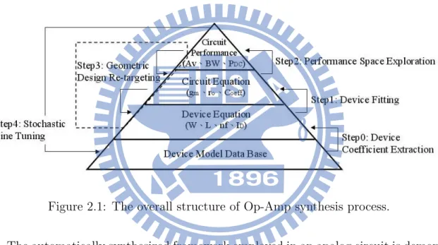
Figure 2.1: The overall structure of Op-Amp synthesis process.
The automatically synthesized framework employed in an analog circuit is demon-strated in this chapter. The prototype of the design flow is shown in Figure 2.1. The synthesis process is divided into two main phases to achieve the optimization, the global search, and the local search. These two phases have their own advantage to guarantee the quality of the optimal solution and the efficiency.
The first phase is the global search. It aimed at the description of actual circuit behavior, the characteristics of each device, and the specification for the expected performance. This process for the prediction of circuit ability could be regarded as an optimization problem, expressed to a convex form of geometric programming [6, 7]. This application for the optimization geometric programming has been widely
used for the analog circuit design [8, 9, 10, 11]. The comparison between the op-timization approaches of this convex method and of others [12, 13, 14] shows that the former deals with solving the problem much more reliably and efficiently. It handles large quantity of design variables and constraints. In addition, it executes the optimization process in polynomial time and guarantees the solution to be truly global.
The second phase is the local search, which is a type of reconstruction of circuit using the simulators of an analog circuit. It makes up the offset of the initial guess taken from the previous optimization phase, which is caused by the incomplete for-mulated design defects. Furthermore, it could adjust the shortcoming of the design, thereby achieving the actual optimum solution. In addition, it works efficiently by starting from the corresponding initial optimum value. On the whole, the optimiza-tion work was done through the two phases to achieve a globally optimized soluoptimiza-tion of the circuit as the initial guess values and then employed the localization fine-tune operation to obtain a reliable synthesis result.
In simple terms, the design sequence of this hierarchical synthesis framework is run under four steps. Step 1 is device fitting, which is an extraction process between the model and the device coefficients of the design equation. Step 2, performance space exploration, and step 3, geometric design retargeting, involve a convex optimization searching of the circuit parameters to satisfy the sets of expectant specification. Step 4, stochastic fine-tuning, is a self-confirm function for the optimum result from the previous steps by localized searching. For instance, in this thesis, steps 1 to 3 ac-complish the construction of circuit equations and the global optimization searching of the initial values, while step 4 causes the results to be closer to the actual value by localized searching.
This thesis is focused on step 2, which is divided into two parts: comparing the performance response under different conditions of process technology or foundry
and understanding the difference of the results in foundry and technology.
2.1
Device Fitting
The first step aims to create a set of equivalent mathematics equation describing each small-signal device parameter by a simulated electronic-feature database. A foundry provides a model to generate the database, which consists of some sets of mapping between the small-signal parameters and the design variables of a single
device. Small-signal parameters include transconductance (gm) and drain
conduc-tance (gd), while design variables include effective channel length (L), width (W ),
and even the number of fingers (nf ). The model simulates the characteristics of the device in different types and temperatures under a range of device dimensions. The simulation depends on the partial characteristics acquired from the sample testing of the manufactured products. The range is limited by the largest and the smallest element length and width of the product. The different models provide different types of mapping. Device fitting aims to extract the mapping relationship from the geometry-level design variables to the circuit-level parameters of a required device. The parameters of each device are described as a function as a combination of design variables: f(X1,...,Xm) = Pn i=1(ciX1i a1iX 2ia2i· · · Xmiami)
f(X1,...,Xm) is the device parameters.
cn is the constant coefficient of the device parameters.
am is the fitting coefficient of design variables.
Xm is the design variables.
The equations above could be transferred into posynomial form by taking logarithm.
It could be reformed as follows: g(X1,...,Xm)=
Pn
i=1(ci+a1iX1i+a2iX2i+...+amiXmi)
aj = log(aj), j = 1, . . . , m
Xj = log(Xj), j = 1, . . . , m
It could be further regarded as a type of geometric program and could form a lean-square error problem to minimize errors such as symbolic analysis or curve fitting [15, 16, 17, 18, 19, 20]. The final form of this fitting process is as follows:
Def ine : D =Pm i=1 di C = Pn i=1(ci+ aiXji), j = 1, . . . , m minimize ||D − C||2 (2.1) (2.2)
The function of C is the circuit-level design variables The function of D is the device-level design variables
Another critical concern is device characteristics as the applications of a device are not ideal. The device may suffer from the impact of parasitic effects. For instance, the parasitic capacitors will result in low bandwidth, leakage of alternating current, and more power losses. The phenomenon could be formulated as follows to feed the actual benefits: Def ine : D =Pm i=1 di P ef f =Pn i=1(ci + aiYki), k = 1, . . . , m minimize ||D − P ef f ||2 (2.3) (2.4)
The function of Peff is the circuit-level parasitic effects of the device.
2.2
Performance Space Exploration
In this step, the overall circuit behavior is expressed, combined with the charac-teristics of the device, in which the fitting coefficients are obtained from the previous step; this allows the device to achieve the performance specification. This explo-ration process could be regarded as a solution to the convex optimization problem. This solution is truly global because of the convex search form. This convex form is a special type of geometric programming; hence, it could be handled by interior point methods [21], even if the function is non-linear. This also allows for a more efficient search operation. Considering the form of the geometric program (in convex form), the equation is constructed through a change in variable and transformation of the objective and constraint function, as follows:
Def ine : D = di, i = 1, . . . , p P ef f = ej, j = 1, . . . , q C = fj, j = 1, . . . , r P er = {gk, k = 1, . . . , s}l,l=1,...,t ej = hCom(D) fj = h Com 2 (D) minimize f0(D, C, P er) subject to dimin ≤ di ≤ dimax fjmin ≤ fj ≤ fjmax gkmin ≤ gk≤ gkmax (2.5) (2.6) Per is the performance metrics
ej is the mapping equations from D to Peff
fj is the mapping equations from D to C
gk is the design equations from C to Per
The objective and subjectivity must be confined to the posynomial functions. A set of performance specifications is regarded as the criteria for the determina-tion of the limits of system performance. It is given to serve as constraints, together
with the objective. Circuit performance includes gain, frequency bandwidth, and power consumption.
2.3
Geometric Design Re-targeting
The third step is a reverse design project for verifying the integrity of the opti-mization system constructed from the previous steps. Designers could find a number of feasible specifications, which will be carried into the optimization system as the constrains, by observing the performance space. The circuit performance covers for the new constraints in order to extract the new circuit parameters and device variables. The result must be close to each other if the circuit behavior is expressed completely.
In theory, this step could directly determine the retargeted value of the device parameters from the performance specifications. This process is divided into two sub-steps to accomplish the work: circuit-level geometric design retargeting and device-level geometric design retargeting. It is anticipated that this will reduce the unexpected effective factors during the retargeting process if we verify the value of the device parameters but ignore that of the circuit.
The goal of the first sub-step is to find the optimal value of the circuit parameters from the given feasible specifications under the previously established optimization system. The problem could be formulated as follows:
Def ine : D = di, i = 1, . . . , p P ef f = ej, j = 1, . . . , q C = fj, j = 1, . . . , r P er = gk, k = 1, . . . , s ej = hCom(D) fj = h Com 2 (D) minimize f0(D, C, P er) subject to fjmin ≤ fj ≤ fjmax gkmin ≤ gk ≤ gkmax (2.7) (2.8)
One of the given specifications for the performance metrics, gkmin and gkmax, and the
specifications, fjmin and fjmax are the constraints for the subject function, except
the specification of the device variables.
The optimal circuit parameters obtained from the previous step are carried into the second sub-step to find the optimal values of the device variables. This process could be formed as follows:
Def ine : D = di, i = 1, . . . , p P ef f = ej, j = 1, . . . , q C = fj, j = 1, . . . , r ej = hCom(D) fj = h Com 2 (D) minimize f (D, P ef f ) subject to dimin ≤ di ≤ dimax fj ≈ fj∗ (2.9) (2.10)
dimin and dimax are the specification of device variables.
fj∗ is the optimal value of circuit parameter, gained from previous step.
The relevant characteristics of the circuit, such as the product of area and the total power consumption, will be described to the object function, related to the device’s variables and parasitic effects.
2.4
Stochastic Fine Tuning
In the final step, the generally optimal value of the device parameters obtained from the previous synthesis process is placed in the simulator as the initial guess. The model is provided by the manufacturer to carry out the actual circuit simula-tion. Some of the initial guess values could not reach actual optimization due to some design defects. The designers could go back to step 3 to fine-tune the design conditions according to the simulated differences of performance between the initial and the actual optimal results.
Chapter 3
Our Implementation on Op-Amp
Synthesis
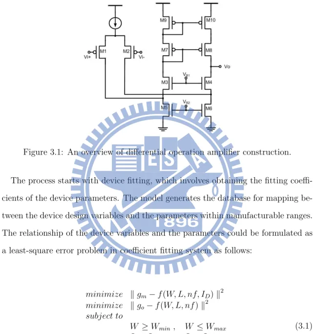
A representative design of a differential Op Amp is shown in Figure 3.1. In
such case, we prefer the single-end double-cascade topologies to achieve high gain and obtain reasonable output swings. There are two types of active component on
this circuit: native (M3, M4, M5, M6) and positive (M1, M2, M7, M8, M9, M10)
metal-oxide semiconductor field effect transistors (MOSFET). The coefficients of the device parameter are extracted from the two model types in step 1, device fitting. In order to simulate the characteristics of device connection, the constraints of swing volt-age and current flow are increased in the framework. The cascade current sources
(M7, M8, M9 and M10) suppress the channel-length modulation effect, which is
inde-pendent of the device Vt and temperature. It will provide mirror current 1/2ID on
each side of the circuit if (W/L)9/(W/L)10 = (W/L)7/(W/L)8. Voltages VB1, VB2
are generated by the current mirror techniques.
Three models of manufacturing technology are involved in the thesis: UMC 90 nm, UMC 65 nm, and TSMC 90 nm mixed-signal CMOS. The variation of these
technologies, such as the mobility of electron and hole (µN, µP) and the capacity of
gate-oxide CoxN, CoxP are also factors of the design equations. The design procedure
hier-archical synthesis in this optimization case is divided into three main steps: device fitting, performance space exploration, and geometric design retargeting.
Figure 3.1: An overview of differential operation amplifier construction.
The process starts with device fitting, which involves obtaining the fitting coeffi-cients of the device parameters. The model generates the database for mapping be-tween the device design variables and the parameters within manufacturable ranges. The relationship of the device variables and the parameters could be formulated as a least-square error problem in coefficient fitting system as follows:
minimize k gm− f (W, L, nf, ID) k2 minimize k go− f (W, L, nf ) k2 subject to W ≥ Wmin , W ≤ Wmax L ≥ Lmin , L ≤ Lmax nf ≥ nfmin , nf ≤ nfmax ID ≥ IDmin , ID ≤ IDmax (3.1)
where gm is the transconductance of the device-level design parameter and go is the
reverse of the output resistance of the device-level design parameter.
parameter in the previous step, the circuit performance (Av, BW, phase margin
(PM), direct current power (PDC) and output power (Pout)) consists of circuit-level
design parameters expressed for the function of device-level design parameters. A reasonable range of each circuit performance is shown in a matrix, searching from the matrix to find the optimal solution of the circuit. The performance-space exploration in this case can be formulated as follows:
Def ine :
Av =
gm1·gm4·gm8 gm8·go4·go6+gm4·go8·go10
Pout = (Vomax − Vomin)
2· g o PDC = 3 · VDD · IDPM8 ω3dB = go Co, go = gm2·gm5 gm2·go4·go5+gm5·go2·go3 P M = pi2 −P2 i=1arctan( ωU GB ωi ) minimize P(Wi · nfi· Li· IDi) subject to
Avi ≥ Avspeci , ω3dBi ≥ ω3dBspeci
Pouti ≥ Poutspeci , PDCi ≤ PDCspeci
Vovi ≥ Vovimin , Vovi ≤ Vovimax
Av ≥ Avmin , Av ≤ Avmax
ω3dB ≥ ω3dBmin , ω3dB ≤ ω3dBmax
Pout ≥ Poutmin , Pout≤ Poutmax
PDC ≥ PDCmin , PDC ≤ PDCmax P M ≥ P Mmin W ≥ Wmin , W ≤ Wmax L ≥ Lmin , L ≤ Lmax nf ≥ nfmin , nf ≤ nfmax ID ≥ IDmin , ID ≤ IDmax (3.2)
PDC is the DC power consumption
Pout is the output power
Av is the voltage gain
P M is defined in terms of the phase of the transfer function at the unity-gain band-width
ω3dB is the cut-off frequency
ωU GB is the unit-gain bandwidth frequency, can be expressed as
ωi is the non-dominant pole frequency. The second and third pole (ω1 and ω2) can be expressed as follows: ω1 = gm7 Ca , Ca = CdbM7 + CgsM7 + gm7 go7 · (CgsM8 + CgdM8) ω2 = gm6 Cb , Cb = CdbM2 + CdgM2 + CdbM6 + CdgM6 + CsgM4 + gm6 go6 · (CsbM4)
go is the output reverse impedance
Co is the output capacitance
Ca is the capacitance at the gate of M7
Cb is the capacitance at the drain of M6
Wi is the width of the transistor
nfi is the number of fingers of the transistor
Li is the length of the transistor
IDi is the drain current of the transistor
A set of each performance specifications - [Avmin, Avmax]j, [ω3dBmin, ω3dBmax]j, [P Mmin, P Mmax]j,
[Poutmin, Poutmax]j, [PDCmin, PDCmax]j, j = 1, . . . , n - on the performance metrics is
considered the constraints for the optimization problem, given the objective func-tion. The objective function in (3.2) is to minimize the overall circuit area and power consumption.
In order to ensure that each transistor is working in the saturation region, the
overdrive voltage Vov is defined in a limited range. The lowest boundary of Vov is
VovM1 ≤ Vref + Vtref − VtM1 − Vi+
VovM2 ≤ Vref + Vtref − VtM2 − Vi−
VovM3 ≤ VB1 + VtM5 − VB2 − VtM3 VovM4 ≤ VB1 + VtM6 − VB2 − VtM4 VovM3 + VovM5 ≤ VB1 − VtM3 VovM4 + VovM6 ≤ VB1 − VtM4 VovM7 + VovM9 ≤ VDD+ VtM3 − VB1− VtM7 − VtM9 VovM8 + VovM10 ≤ VDD + VtM4 − VB1 − VtM8 − VtM10 VovM7 = VovM8 VovM9 = VovM10 (3.3)
VovM ? is the function of W, L, nf, ID, mobility µ and oxide capacitor Cox
Each Vov is the function of W, L, nf and ID, which could be expressed as follows:
V2
ovMn =
2·IDMn·LMn
µMn·CoxMn·WMn·nfMn, n = 1, · · · 10 (3.4)
The limit of the output swing is VDD− VGS9 − VGS7 + VtM 8. Inserting additional
cascade devices in each branch will cause more gain but will further limit the out-put swing, which will make it more difficult to design each device working in the saturation region.
Geometric-design retargeting ensures that the optimization in the previous steps is effective. It is divided into two sub-steps. The goal of the first sub-step, which is called circuit-level geometric design retargeting, is to find the optimal values
of the device (gm, go) from a given specification of performance metrics under the
optimization problem used in the previous step. The problem formulation can be formed as follows:
Def ine :
Av =
gm1·gm4·gm8 gm8·go4·go6+gm4·go8·go10
Pout = (V omax− V omin)2· go
PDC = 3 · VDD · IDPM8 ω3dB = go Co, go = gm2·gm5 gm2·go4·go5+gm5·go2·go3 P M = pi2 −P2 i=1arctan( ωU GB ωi ) minimize P(Wi · nfi· Li· IDi) subjectto gm ≤ gmmax , gm ≥ gmmin go ≤ gomax , go ≥ gomin Av ≥ Avspec , ω3dB ≥ ω3dBspec
Pout ≥ Poutspec , PDC ≤ PDCspec
P M ≥ P Mmin
(3.5)
The second sub-step, which is called device-level geometric design retargeting,
aims to find the optimal value of W, L, nf, and ID of each single transistor obtained
in the circuit-level geometric design retargeting. The problem formulation can be generally written as follows:
minimize P(Wi· nfi· Li· IDi) subjectto gmi ≈ g ∗ mi , goi ≈ g ∗ oi W ≥ Wmin , W ≤ Wmax L ≥ Lmin , L ≤ Lmax nf ≥ nfmin , nf ≤ nfmax ID ≥ IDmin , ID ≤ IDmax (3.6)
gm∗ is the optimal trans-conductance acquired from previous sub step.
Chapter 4
Experimental Results
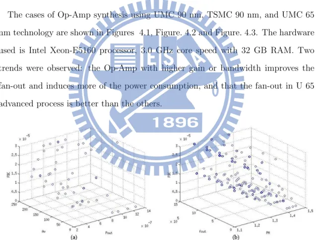
The cases of Op-Amp synthesis using UMC 90 nm, TSMC 90 nm, and UMC 65 nm technology are shown in Figures 4.1, Figure. 4.2 and Figure. 4.3. The hardware used is Intel Xeon-E5160 processor, 3.0 GHz core speed with 32 GB RAM. Two trends were observed: the Op-Amp with higher gain or bandwidth improves the fan-out and induces more of the power consumption, and that the fan-out in U 65 advanced process is better than the others.
Figure 4.1: The performance space under UMC90nm technology.
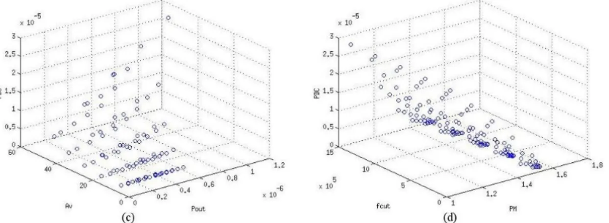
The relationship between power consumption and gain response of the circuit on each technology is as shown in Figure 4.1 (a), 4.2 (c) and 4.3 (e), while the rela-tionship between power consumption and frequency response is as shown in Figure
Figure 4.2: The performance space under TSMC90nm technology.
Figure 4.3: The performance space under UMC65nm technology.
4.1(b), 4.2 (d) and 4.3 (f). For the example of Figure 4.1, there are a total of 3125 points obtained from performance exploration in (a) and (b), while each point indi-cates a result of optimization. Due to the relationship of trade-off between gain and bandwidth, the set of regional points with relatively higher gain must be obtained from (a), and the set of regional points with relatively higher cut-off frequency must be obtained from (b) under same conditions of power consumption, output power and phase margin in order to figure out the most appropriate points in accordance with the judgement rules of low power consumption, high output power and high phase margin.
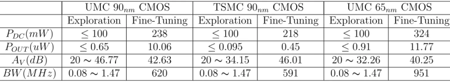
in Table 4.1. The coefficients extraction of device fitting parameters is shown in Ta-bles 4.2-4.4, which simulation result is shown in Table 4.5. In Table 4.1, it shows that from the previous bottom-up design procedures, an optimization space of cir-cuit performance can be calculated efficiently, but which is not correspondent with one calculated via the simulation method actually. Using the simulation method to find out optimal solutions will consume a lot of time. Therefore, Table 4.6 shows that as estimating a simulation optimal solution in this space of circuit performance via the top-down fine-tuning method, the time can be shortened. And the solution can also be as exact as the solution found out via the simulation method.
Table 4.1: SUMMARY OF STEP 2, MAPPING BETWEEN CIRCUIT PARAME-TERS AND PERFORMANCE METRICS.
Technology UMC 90nm CMOS TSMC 90nm CMOS UMC 65nm CMOS
PDC(mW ) ≤ 100 ≤ 100 ≤ 100
POU T(uW ) ≤ 0.65 ≤ 0.095 ≤ 0.91
AV(dB) 20 ∼ 46.77 20 ∼ 34.15 20 ∼ 32.26
BW (M Hz) 0.08 ∼ 1.47 0.08 ∼ 1.47 0.08 ∼ 1.47
P M (rad) 0.5236 ∼ 1.0472 0.5236 ∼ 1.0472 0.5236 ∼ 1.0472
Table 4.2: DEVICE FITTING PARAMETERS (gm)
UMC 90nm TSMC 90nm UMC 65nm
NMOS PMOS NMOS PMOS NMOS PMOS
coef f. 66.5443 21.13 62.9751 30.8794 4.8847 4.0834
W 0.3922 0.4707 0.6369 0.6904 0.528 0.5255
L 1.3E-8 -6.93E-9 3.72E-9 4.16E-8 1.49E-8 4.42E-9
nf -3.19E-8 -3.19E-8 2.77E-10 -1.35E-8 -1.68E-8 -9.05E-9
ID 0.5836 0.4985 0.3681 0.3156 0.2892 0.307
The comparison of the circuit performance in step 3, performance exploration, and step 4, stochastic fine-tuning, is shown in Table 4.6. The simulation result from the initial guesses is close to the value of fine-tuning. The performance of fine-tuning
Table 4.3: DEVICE FITTING PARAMETERS (Resist.)
UMC 90nm TSMC 90nm UMC 65nm
NMOS PMOS NMOS PMOS NMOS PMOS
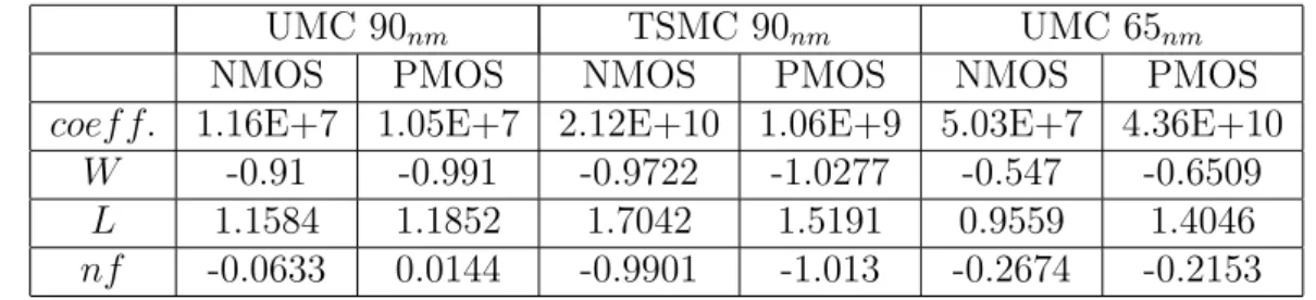
coef f. 1.16E+7 1.05E+7 2.12E+10 1.06E+9 5.03E+7 4.36E+10
W -0.91 -0.991 -0.9722 -1.0277 -0.547 -0.6509
L 1.1584 1.1852 1.7042 1.5191 0.9559 1.4046
nf -0.0633 0.0144 -0.9901 -1.013 -0.2674 -0.2153
is better than that of the initial guesses. The experiments confirmed that each set of synthesis of performance space exploration could be accomplished within a few minutes, in the case of hundreds of variables and constraints.
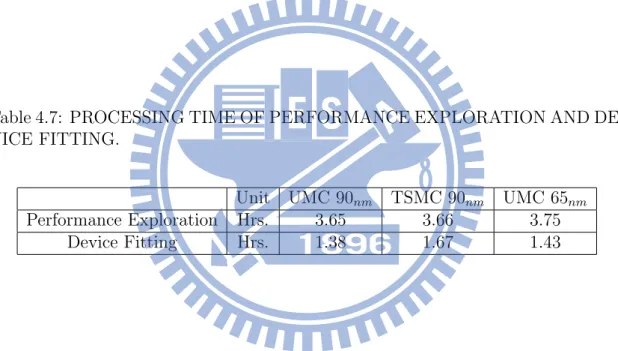
The processing time of performance exploration and device fitting are shown as table 4.7. The samples of performance exploration for each technology are 3125 sets. For the model difference, such as the margin of device corner, the samples of device fitting are about thousands to ten thousand for each technology. On the other hand, more samples will enhance more accuracy of device fitting and require more runtime.
Table 4.4: DEVICE FITTING PARAMETERS (Cap.)
UMC 90nm TSMC 90nm UMC 65nm
NMOS PMOS NMOS PMOS NMOS PMOS
Cdg coef f. 0.028 0.029 0.2793 3.3299 0.0572 0.0057 W 1.6656 1.6368 1.7193 1.8859 1.702 1.6185 L 0.8449 0.8827 0.973 0.9865 0.856 0.783 nf 0.0989 0.0839 1 1 0.0666 0.0886 Cdb
coef f. 2.34E-6 2.0E-4 4.96E-16 7.09E-21 5.70E-10 1.21E-9
W 0.6823 1.1019 -0.518 -1.2254 0.7149 0.6502 L 1.1896 1.1089 1.0415 0.9895 0.5506 0.7253 nf -0.0775 -0.1971 1 1 0.2068 0.2127 Cgs coef f. 0.2132 0.0867 8.2999 89.6328 2.5552 0.1064 W 1.2859 1.2568 1.4586 1.6209 1.444 1.3075 L 0.8978 0.8761 0.9956 0.9913 0.8871 0.815 nf 0.0701 0.0983 1 1 0.0487 0.0765
Table 4.5: SIMULATOR RESULT.
Technology UMC 90nm CMOS TSMC 90nm CMOS UMC 65nm CMOS
AV(dB) 41.16 38.14 45.02
GBW (M Hz) 190 52.66 140.42
P hase -119.8 -95.3 -106.4
P haseM argin 60.2 84.7 73.65
Table 4.6: PERFORMANCE COMPARISON TO STEP 3, PERFORMANCE EX-PLORATION AND STEP 4, STOCHASTIC FINE-TUNING.
UMC 90nm CMOS TSMC 90nm CMOS UMC 65nm CMOS
Exploration Fine-Tuning Exploration Fine-Tuning Exploration Fine-Tuning
PDC(mW ) ≤ 100 238 ≤ 100 218 ≤ 100 324
POU T(uW ) ≤ 0.65 10.06 ≤ 0.095 0.45 ≤ 0.91 11.77
AV(dB) 20 ∼ 46.77 42.63 20 ∼ 34.15 46.01 20 ∼ 32.26 40.25
Table 4.7: PROCESSING TIME OF PERFORMANCE EXPLORATION AND DE-VICE FITTING.
Unit UMC 90nm TSMC 90nm UMC 65nm
Performance Exploration Hrs. 3.65 3.66 3.75
Chapter 5
Conclusion
In this thesis, the hierarchical synthesis methodology was applied in the Op Amp circuit design to achieve sizing optimization. Base on the simplified amendment pro-cedure of framework for each different technology application, the good preliminary solution could be obtained from excellent execution efficiency.
Bibliography
[1] K.-H. Meng, P.-C. Pan, and H.-M. Chen, “Integrated hierarchical synthesis of analog/rf circuits with accurate performance mapping,” in International Sym-posium Quality Electronic Design (ISQED), pp. 1 – 8, March 2011.
[2] P. Mandal and V. Visvanathan, “Cmos op-amp sizing using a geometric pro-gramming formulation,” IEEE Transactions on Computer-Aided Design of In-tegrated Circuits and Systems, pp. 22 – 38, Jan. 2001.
[3] P. C. Maulik and L. R. Carley, “Automating analog circuit design using constrained optimization techniques,” in IEEE International Conference on Computer-Aided Design (ICCAD), pp. 390 – 393, Nov. 1991.
[4] W. Daems, G. Gielen, and W. Sansen, “Simulation-based generation of posyn-omial performance models for the sizing of analog integrated circuits,” IEEE Transactions on Computer-Aided Design of Integrated Circuits and Systems, pp. 517 – 534, May 2003.
[5] M. del Mar Hershenson, S. P. Boyd, and T. H. Lee, “Gpcad: a tool for cmos op-amp synthesis,” in IEEE/ACM International Conference on Computer-Aided Design (ICCAD), pp. 296 – 303, Nov. 1998.
[6] “Cvx research.” http://cvxr.com.
[7] B. Razavi, Design of Analog CMOS Integrated Circuits. McGraw Hill, 1 ed., 2001.
[8] M. del Mar Hershenson, “Cmos analog circuit design via geometric program-ming,” in Proceedings of the 2004 American Control Conference, pp. 3266 – 3271 vol.4, July 2004.
[9] D. Li, G.-H. Shu, and M.-T. Rong, “Tradeoff design for analog integrated cir-cuits via geometric programming,” in IEEE 8th International Conference on ASIC, pp. 824 – 826, Oct. 2009.
[10] M. Maghami, F. Inanlou, and R. Lotfi, “Simulation-equation-based methodol-ogy for design of cmos amplifiers using geometric programming,” in IEEE In-ternational Conference on Electronics, Circuits and Systems (ICECS), pp. 360 – 363, Sept. 2008.
[11] P. K. Meduri and S. K. Dhali, “A framework for automatic cmos opamp sizing,” in IEEE International Midwest Symposium on Circuits and Systems (MWS-CAS), pp. 608 – 611, Aug. 2010.
[12] M. del Mar Hershenson, S. P. Boyd, and T. H. Lee, “Optimal design of a cmos op-amp via geometric programming,” IEEE Transactions on Computer-Aided Design of Integrated Circuits and Systems, Jan. 2001.
[13] K. Doganis, K. Walsh, and P. Linardes, “Synthesis of analog asics using opti-mization in conjunction with circuit simulation techniques,” in Second Annual IEEE ASIC Seminar and Exhibit, pp. 1 – 5, Sep. 1989.
[14] A. Sallem, M. Fakhfakh, E. Tlelo-Cuautle, and M. Loulou, “Multi-objective simulation-based optimization for the optimal design of analog circuits,” in International Conference on Microelectronics (ICM), pp. 1 – 4, Dec. 2011. [15] J. Kim, L. Jaeseo, L. Vandenberghe, and C.-K. K. Yang, “Techniques for
optimization,” in IEEE/ACM International Conference on Computer Aided Design, pp. 863 – 870, Nov. 2004.
[16] T. Eeckelaert, W. Daems, G. Gielen, and W. Sansen, “Generalized posynomial performance modeling,” in Design, Automation and Test in Europe Conference and Exhibition, pp. 250 – 255, 2003.
[17] W. Daems, G. Gielen, and W. Sansen, “An efficient optimization-based tech-nique to generate posynomial performance models for analog integrated cir-cuits,” in Design Automation Conference, pp. 431 – 436, 2002.
[18] W. Daems, G. Gielen, and W. Sansen, “A fitting approach to generate symbolic expressions for linear and nonlinear analog circuit performance characteristics,” in Proceedings Design, Automation and Test in Europe Conference and Exhibi-tion, pp. 268 – 273, 2002.
[19] W. Sansen, G. Glelen, and H. Walscharts, “A symbolic simulator for analog circuits,” in IEEE International Solid-State Circuits Conference, pp. 204 – 205, Feb. 1989.
[20] G. Gieleu, G. Debyser, P. Wambacq, I. Swings, and W. Sansen, “Use of sym-bolic analysis in analog circuit synthesis,” in IEEE International Symposium on Circuits and Systems (ISCAS), pp. 2205 – 2208 vol.3, Apr - 3 May 1995. [21] S. J. Wright, “Structured interior point methods for optimal control,” in IEEE