以感應耦合式電漿系統成長之超薄氮氧化矽薄膜的電特性與可靠度研究
90
0
0
全文
(2) 以感應耦合式電漿系統成長之超薄氮氧化矽薄膜的 電特性與可靠度研究 The Electrical Characteristics and Reliability of Ultrathin Oxynitride Grown by ICP Plasma. 學生:陳柏寧. Student:Bo-Ning Chen. 指導教授:張國明 博士. Advisor:Dr. Kow-Ming Chang. 桂正楣 博士. Dr. Cheng-May Kwei. 國立交通大學電子工程學系電子研究所碩士班 碩士論文. A Thesis Submitted to Institute of Electronics College of Electrical Engineering and Computer Science National Chiao Tung University In Partial Fulfillment of the Requirements for the Degree of Master of Science In Electronics Engineering June 2004 Hsinchu, Taiwan, Republic of China 中華民國九十三年六月.
(3) 以感應耦合式電漿系統成長之超薄氮氧化矽薄膜的電 特性與可靠度研究 研究生:陳柏寧. 指導教授:張國明 博士 桂正楣 博士. 國立交通大學 電子工程學系 電子研究所碩士班. 摘. 要. 當互補式金氧半場效電晶體的閘極通道長度微縮到 90 奈米以下時,閘極介 電層的有效電性厚度將縮小至 1.5 奈米以下,但是達此超薄厚度之二氧化矽絕緣 膜其直接穿遂電流將大到無可忍受的程度,另外,隨著製程熱預算的降低,低溫 氧化製程技術的必要性也隨之增加。在本論文中,我們首次提出在 300 ℃的低溫 環境下,使用感應耦合式 (ICP) N2O 電漿氧化成長 1 nm 超薄氮氧化矽 (oxynitride) 薄膜,藉由改變電漿功率和處理時間以獲得最佳的製程條件,又以不同氮氣與氧 氣組成比例的電漿來成長氮氧化矽薄膜並與氧氣電漿形成的二氧化矽薄膜作比 較。接著,我們更進一步的發展感應耦合式氮氣電漿氮化處理的方法以改善原先 形成的氮氧化矽之電特性與可靠度,對氮化處理的製程時間和氣體組成探討以找 出最佳的氮化條件,最後證實,感應耦合式電漿系統在 300 ℃的低溫環境下,以 200 瓦的感應耦合式 N2O 電漿處理 1 分鐘後形成的氮氧化矽薄膜有最佳的電性與 可靠度,而且再加以 200 瓦的感應耦合式氮氣電漿氮化處理後,可得到進一步的 改善。1.0 nm 的氮氧化矽薄膜有 1.8 µF/cm2 的高電容值,與在-1 V 電壓操作下漏 電僅 0.1 A/cm2 的特性,此閘極介電薄膜將可應用在下世代高性能的 65 奈米互補 式金氧半導體電晶體元件中。 i.
(4) The Electrical Characteristics and Reliability of Ultrathin Oxynitride Grown by ICP Plasma. Student:Bo-Ning Chen. Advisor:Kow-Ming Chang Cheng-May Kwei. Institute of Electronics National Chiao Tung University. ABSTRACT. When the gate oxide thickness scales down to 1.0 nm regime, the direct-tunneling current becomes main key issue for high-performance CMOS beyond 90 nm. On the other hand, in order to avoid dopant redistribution, the low-temperature oxidation process becomes more important while device size continuously scales down. In this study, the high-quality silicon oxynitride (SiON) gate dielectric with physical thickness 1.0 nm grown by ICP N2O plasma at a low temperature of 300℃ has been developed. The optimum process condition was found by adjusting the plasma power, process time and pressure. Then, the experimental results were compared with other oxynitrides grown by various gas flow ratios of N2/O2 plasma and ICP O2 plasma grown pure SiO2. The experiment results showed that 1.0nm oxynitride grown by ICP N2O plasma at RF power of 200 W for 1 min has the highest capacitance density of 1.8 µF/cm2 and the lowest leakage current density of 0.1 A/cm2. Furthermore, we used ICP plasma nitridation technique to further improve the ii.
(5) electrical characteristics and reliability of oxynitride. The process time and the composition of N2 and Ar/He mixed plasma were investigated to find the optimum nitridation condition. The experiment results showed that the optimum condition of plasma nitridation process is ICP N2/He mixed plasma at RF power of 200 W for 5 min. Hence, the high-quality and low-leakage 1.0 nm ultrathin oxynitride grown by ICP-plasma at a low temperature as 300 ℃ is suitable to be applied as gate dielectric of next-generation high-performance 65 nm MOSFET devices.. iii.
(6) 致謝. 回顧在交大電子所碩士班兩年來的學習生活,首先感謝指導教授張國明教授 與桂正楣教授對我的諄諄教誨,給予我在研究生活中重大幫助。另外感謝一直不 斷指導我實驗的楊文誌學長,楊文誌學長在自己即將畢業而分身乏術時,仍然熱 心地對我的碩士論文及口試提出寶貴的建議,我能夠完成碩士班的研究很大一部 份有賴於此。 在兩年之中,實驗室的各位學長、同學與及學弟,常在研究與生活上給予我 各種幫助,交大電子所其他實驗室的學長與同學們,對我的友情也讓我獲益良 多。還有國家毫微米實驗室和交大奈米中心各位研究人員在維護實驗環境上的努 力,才使我得以完成實驗。 最後,我要感謝家人對我的支持,母親、姊姊和妹妹的愛與關懷是我最重要 的寶物,最後,感念我的父親,相信他一定會為我高興。. iv.
(7) Contents Chinese Abstract ...........................................................................................................i English Abstract ...........................................................................................................ii Acknowledgment ..........................................................................................................iv Contents .......................................................................................................................v Table Captions ........................................................................................................... viii Figure Captions.............................................................................................................ix. Chapter 1 Introduction......................................................................................................................................1. 1.1 Overview of ultrathin oxide technology………………….................................……………………...…1 1.2 Alternative gate dielectrics for advanced CMOS technology..……………..................………3 1.2.1 High-k dielectric materials…………………………………………… …………………………………3 .. 1.2.2 Silicon nitride, N/O stack, and oxynitride……………………..…………………………………4 1.3 Others oxynitridation techniques for gate dielectrics………….......................…………………...5 1.3.1 Rapid thermal process (RTP)..……………………………………..……………...……………………5 1.3.2 Jet vapor desposition (JVD)……………………………...…………..…………………………………5 1.3.3 Nitrogen implant……………………..…………………………………………………………………….…6 1.3.4 Plasma nitridation treatment……………………..………………………………………………......…7 1.4 Motivation ……………………………………………………………........................................................……………7 1.5 Thesis outline…………………………………......................................................………………………………...…9 1.6 References ………………………………………........................................................…………………………….…11. Chapter 2 The Fabrication of Ultrathin 1.0 nm-thick Oxynitride Film...........................................................................................................................................................................................18 v.
(8) 2.1 The fabrication of capacitor with 1.0 nm oxynitride film.........................................................18 2.2 Devices measurement method........................................................................................................................20 2.2.1 Determination of gate dielectric thickness.................................................................................20 2.2.2 C-V and J-V measurement......................................................................................................................22 2.2.3 Determination of reliability……….…...................................................................................................25 2.3 References......................................................................................................................................................................27. Chapter 3 The Study of Ultrathin Oxynitride Grown by Using HD-ICP Plasma……….…........................................................................................................................................29. 3.1 The dependence of the ultrathin oxynitride thickness..................................................................29 3.2 The electrical characteristics of 1.0 nm ultrathin oxynitride films.....................................31 3.2.1 The electrical characteristics of 1.0 nm ultrathin oxynitride films grown by different power of ICP N2O Plasma...............................................................................................31 3.2.2 The electrical characteristics of 1.0 nm ultrathin oxynitride films grown by different gas composition.......................................................................................................................32 3.2.3 The nitrogen concentration of oxynitride grown by high-density ICP N2O plasma......................................................................................................................................................................33 3.3 The reliability of 1.0 nm ultrathin oxynitride films........................................................................34 3.3.1 The reliability of 1.0 nm ultrathin oxynitride films grown by different power of ICP N2O plasma......................................................................................................................................34 3.3.2 The reliability of 1.0 nm ultrathin oxynitride films grown by different composition of ICP plasma...................................................................................................................35 3.4 Summary.........................................................................................................................................................................36 3.5 References......................................................................................................................................................................37. vi.
(9) Chapter 4 The ICP-Plasma Nitridation Effect on Electrical Characteristics and Reliability of 1.0 nm Ultrathin Oxynitride...........39. 4.1 The improvement to the electrical characteristics by different time of ICP N2 plasma nitridation..............................................................................................................................................................39 4.1.1 The improvement to the electrical characteristics by different time of ICP N2 plasma nitridation.........................................................................................................................................40 4.1.2 The improvement by ICP N2 plasma nitridation to the electrical characteristics of oxynitride grown by different plasma....................................................................................41 4.1.3 The improvement to the electrical characteristics by different concentration of ICP N2 plasma nitridation......................................................................................................................41 4.2 The Improved reliability of 1.0 nm ultrathin oxynitride films...............................................42 4.2.1 The improvement of the reliability by different time of ICP N2 plasma nitridation...........................................................................................................................................................42 4.2.2 The improvement by ICP N2 plasma nitridation to the reliability of oxynitride grown by different plasma.....................................................................................................................43 4.2.3 The improvement to the reliability by different concentration of ICP N2 plasma nitridation........................................................................................................................................44 4.3 Summary.........................................................................................................................................................................45 4.4 References...................................................................................................................................................................46. Chapter 5 Conclusions.....................................................................................................................................47. vii.
(10) Table Captions. Chapter 3. Table 3-1 The thickness of oxynitride films versus working pressure. Table 3-2 The thickness of oxynitride versus plasma power. Table 3-3 The thickness of oxynitride versus processing time. viii.
(11) Figure Captions Chapter 2. Fig. 2-1 The ICP system that was used in this experiment.. Fig. 2-2 The experimental procedure of ICP plasma oxynitridation process.. Fig.2-3 The detail fabrication process flow of MOS Capacitor with 1.0 nm oxynitride. Fig 2-4 Principles of an ellipsometric measurement. Fig 2-5 Spectroscopic ellipsometry measured SiO2 film thickness vs. thickness measured by, XPS, C–V analysis, and TEM.. Fig 2-6 Schematic illustration of (a) FN-tunneling and (b) direct tunneling mechanisms of electron flow through an oxide potential barrier of height ΦB.. Chapter 3. Fig. 3-1 The dependence of oxide thickness on chamber pressure.. Fig. 3-2 The dependence of oxide thickness on RF power.. Fig. 3-3 The dependence of oxide thickness on oxidation time.. ix.
(12) Fig. 3-4 High-resolution cross-sectional TEM photograph of MOS capacitor with 1.0 nm thick oxynitride gate dielectric. The capacitor was formed by depositing 100 nm ploy-Si/1 nm oxsynitride on Si substrate.. Fig. 3-5 Enlarged high-resolution TEM micrographs of 1 nm oxynitride sample for the polysilicon-oxynitride-silicon structure.. Fig. 3-6 The high-frequency (100 kHz) C-V curves of MOS capacitors with 1.0 nm gate dielectrics grown by HD-ICP N2O-plasma at various RF powers.. Fig. 3-7 The current density versus gate voltage (Jg-Vg) characteristics of the 1.0 nm gate dielectrics grown by HD-ICP N2O-plasma at various RF powers.. Fig. 3-8 The high-frequency (100 kHz) C-V curves of MOS capacitors with 1.0 nm gate dielectrics grown by HD-ICP N2O, O2, and N2/O2-mixture-plasma at RF power of 200 W, respectively.. Fig. 3-9 The current density versus gate voltage (Jg-Vg) characteristics of the 1.0 nm gate dielectrics grown by HD-ICP N2O, O2, and N2/O2-mixture-plasma at RF power of 200 W, respectively.. Fig. 3-10 The SIMS nitrogen profiles of the 1.0 nm gate dielectric films of the 1.0 nm gate dielectrics grown by HD-ICP N2O and N2/O2-mixture-plasma at RF power of 200 W, respectively. Fig. 3-11 The charge trapping characteristics by monitoring the change in gate voltage (ΔVg) as a function of stress time for 1.0 nm oxynitride films grown by HD-ICP x.
(13) N2O-plasma at various RF powers.. Fig. 3-12 Stress-induced leakage current (SILC) of capacitors with 1.0 nm oxynitride films grown by HD-ICP N2O-plasma at various RF powers.. Fig. 3-13 Charge-to-breakdown characteristics (Qbd) of the oxynitride films grown by HD-ICP N2O-plasma at various RF powers under constant current stress (J = -1 A/cm2).. Fig. 3-14 The charge trapping characteristics by monitoring the change in gate voltage (ΔVg) as a function of stress time for 1.0 nm oxynitride films grown by HD-ICP N2O, O2, and N2/O2-mixture-plasma at RF power of 200 W, respectively.. Fig. 3-15 Stress-induced leakage current (SILC) of capacitors with 1.0 nm oxynitride films grown by HD-ICP N2O, O2, and N2/O2-mixture-plasma at RF power of 200 W, respectively.. Fig. 3-16 Charge-to-breakdown characteristics (Qbd) of the oxynitride films grown by HD-ICP N2O, O2, and N2/O2-mixture-plasma at RF power of 200 W, respectively under constant current stress (J = -1 A/cm2).. xi.
(14) Chapter 4. Fig. 4-1 The experimental procedure of HD-ICP nitridation-plasma process. Fig. 4-2 The high-frequency (100 kHz) C-V curves of MOS capacitors with 1.0 nm gate dielectrics nitrided by HD-ICP N2-plasma with different nitridation-time.. Fig. 4-3 The current density versus gate voltage (Jg-Vg) characteristics of the 1.0 nm gate dielectrics nitrided by HD-ICP N2-plasma with different nitridation-time.. Fig. 4-4 The SIMS nitrogen profiles of the 1.0 nm gate dielectric films of the 1.0 nm gate dielectrics nitrided by HD-ICP N2-plasma with different nitridation-time.. Fig. 4-5 The high-frequency (100 kHz) C-V curves of MOS capacitors with the 1.0 nm gate dielectrics grown by HD-ICP N2O, O2, and N2/O2-mixture-plasma with and without nitridation, respectively.. Fig. 4-6 The current density versus gate voltage (Jg-Vg) characteristics of 1.0 nm gate dielectrics grown by HD-ICP N2O, O2, and N2/O2-mixture-plasma with and without nitridation, respectively.. Fig. 4-7 The high-frequency (100 kHz) C-V curves of MOS capacitors with the 1.0 nm. gate. dielectrics. nitrided. by. HD-ICP. N2/He-mixture-plasma, respectively.. xii. N2O,. N2/Ar-mixture,. and.
(15) Fig. 4-8 The current density versus gate voltage (Jg-Vg) characteristics of the 1.0 nm gate dielectrics nitrided by HD-ICP N2O, N2/Ar-mixture, and N2/He-mixture-plasma, respectively.. Fig. 4-9 The charge trapping characteristics by monitoring the change in gate voltage (ΔVg) as a function of stress time for 1.0 nm oxynitride films nitrided by HD-ICP N2-plasma with different nitridation-time.. Fig. 4-10 Stress-induced leakage current (SILC) of capacitors with 1.0 nm oxynitride films nitrided by HD-ICP N2-plasma with different nitridation-time.. Fig. 4-11 Charge-to-breakdown characteristics (Qbd) of the oxynitride films nitrided by HD-ICP N2-plasma with different nitridation-time.. Fig. 4-12 The charge trapping characteristics by monitoring the change in gate voltage (ΔVg) as a function of stress time for 1.0 nm oxynitride films grown by HD-ICP N2O, O2, and N2/O2-mixture-plasma with and without nitridation, respectively.. Fig. 4-13 Stress-induced leakage current (SILC) of capacitors with 1.0 nm oxynitride films grown by HD-ICP N2O-plasma with and without nitridation.. Fig. 4-14 Stress-induced leakage current (SILC) of capacitors with 1.0 nm oxynitride films grown by HD-ICP O2-plasma with and without nitridation.. Fig. 4-15 Stress-induced leakage current (SILC) of capacitors with 1.0 nm oxynitride films grown by HD-ICP N2/O2-mixture-plasma with and without nitridation. xiii.
(16) Fig. 4-16 Charge-to-breakdown characteristics (Qbd) of the oxynitride films grown by HD-ICP N2O, O2, and N2/O2-mixture-plasma with and without nitridation, respectively.. Fig. 4-17 The charge trapping characteristics by monitoring the change in gate voltage (ΔVg) as a function of stress time for 1.0 nm oxynitride films nitrided by HD-ICP N2O, N2/Ar-mixture, and N2/He-mixture-plasma, respectively.. Fig. 4-18 Stress-induced leakage current (SILC) of capacitors with 1.0 nm oxynitride films nitrided by HD-ICP N2O, N2/Ar-mixture, and N2/He-mixture-plasma, respectively.. Fig. 4-19 Charge-to-breakdown characteristics (Qbd) of the oxynitride films nitrided by HD-ICP N2O, N2/Ar-mixture, and N2/He-mixture-plasma, respectively.. xiv.
(17) Chapter 1 Introduction. 1.1 Overview of ultrathin oxide technology. The device size of metal-oxide-semiconductor field effect transistors (MOSFETs) is still scaling down. And the thickness of gate insulator needs to be thinner to maintain the “on” current of the MOSFET [1]-[3]. Silicon dioxide (SiO2) is a most important insulating material in metal-oxide semiconductor (MOS) device technology.. According. to. the. International. Technological. Roadmap. for. Semiconductors (ITRS) [4], an equivalent silicon dioxide thickness of less than 2.0 nm will be required for sub-100 nm generation MOS device. Although there was a concern proposed in 1998 that TDDB (Time Dependent Dielectric Breakdown) will limit the SiO2 gate insulator reduction at the thickness = 2.2 nm [5], recent experimental models suggest that TDDB would work until the thickness of SiO2 is from 1.5 nm to 1.0 nm [6]-[8]. From the results of above research, SiO2 gate insulator would be used until the 30 nm gate length generation for high speed CPUs (central processing units). Several physical limiting factors associated with the ultrathin gate oxides have been identified, including: (a) the direct tunneling current is the most sensitive one to the oxide thickness [9], [10]. As the thickness of the oxide layer decreases, the tunneling current increases in an exponential manner. This increased leakage current not only adversely affects the performance of MOS device but also greatly increases the standby power consumption of a highly integrated chip [9], [10]. (b) Quantum mechanical effects in the substrate [11], 1.
(18) which results from charge confinement in the substrate near the Si/SiO2 interface [12]. (c) Polysilicon depletion effects (PDE) [13], it reduces inversion charge density and transconductance, especially for very-thin oxide MOS devices. Using metallic material for gate electrode should be the most effective way to solve PDE [14]. (d) Oxide reliability [15], [16]: Electrons traveling is a contentious issue concurrently. Electrons traveling through the SiO2 layer may create defects such as electron traps and interface states that in turn, upon accumulation to some critical density, degrade the insulating properties of the oxide [17]. (e) Boron penetration [18], [19]. p+-polycrystalline silicon (p+-polysilicon) gate electrodes have been used instead of n+-polysilicon ones for p-channel MOSFETs to convert the buried-channel operations to surface-channel ones [20]. However, boron penetration from p+-polysilicon gates through such thin gate oxide layers has become a severe problem [21], [22] because of the high carrier activation in the polysilicon is simultaneously required to prevent the gate depletion effect, which degrades the drivability of devices. Therefore, the limitation of the process window must be clarified to fabricate p+-polysilicon gates. And when boron penetration occurs [23], [24], transistors were found to suffer from flat-band voltage (Vfb) shift, threshold voltage (Vt) instability, drive current reduction, and subthreshold slope degradation. So, it is very necessary to study highly reliable ultrathin gate dielectric. In order to grow the high quality ultrathin gate dielectric, there are two kinds of main research directions: (a) one is focus at the material of the gate dielectric, like high-k (high dielectric constant) materials [25], silicon nitride [26], N/O stacks [27], and oxynitride [28]. (b) And another is focus at the process technologies, like: rapid thermal processing (RTP) [29]-[31], jet vapor deposition (JVD) [32], nitrogen implantation [33], and plasma treatment [34], [35], etc.. 2.
(19) 1.2 Alternative gate dielectrics for advanced CMOS technology. 1.2.1 High-k dielectric materials. With the continuous downscaling of CMOS device, the gate-oxide thickness must decrease accordingly drivability improvement and better short channel effect control. Direct tunneling current increases exponentially with the reduction of oxide thickness and it becomes a major portion of the off-state current. In order to achieve a lower gate leakage current, high dielectric constant materials have been proposed to replace SiO2, with greater physical thickness while maintaining the same capacitance [35]-[37]. Typically, high-k dielectric layers are deposited using ALD or MOCVD with, at present, a prime emphasis on Hf-based high-k dielectrics, either as pure HfO2, as silicate or mixed with Al2O3. In some cased nitrogen is added to improve the high-temperature stability. Depending on the deposition conditions ALD as well as MOCVD show serious deficiencies in terms of film closure and material density for ultrathin (< 3 nm) films. Various surface preparation methods and deposition conditions are used to improve the film quality. Detailed studies on the film growth and its evolution requires the use of many analytical methods such as Rutherford Backscattering Spectrometry, Low Energy Ion Scattering, Time-of-flight SIMS, (spectroscopic) ellipsometry and X-ray photoelectron spectroscopy. When trying to correlate the results in terms of film thickness, apparent discrepancies can be observed which relate to nonhomogeneous growth and reduced material density. High-k films allow the use of a physically thicker film while acting electrically as a thin dielectric. Thus, the leakage could be suppressed obviously. However, a trade-off exists since the 3.
(20) band gap, or more importantly the barrier height tends to decrease with increasing dielectric constant. Unfortunately, most of these materials are not thermally stable on silicon and tend to form an interfacial SiOx film to reduce their effective capacitance. Furthermore, there are still these problems of integrating these materials into ever more complicated device processing.. 1.2.2 Silicon nitride, N/O stack, and oxynitride. Silicon nitride is an attractive candidate for gate dielectric due to its relatively high dielectric constant. Further, nitride is an efficient diffusion barrier which can minimize the boron penetration problems, encountered for p+-polysilicon gate integration. However, a single silicon nitride layer may not be suitable to gate dielectric application due to a much degraded device performance as a result of high density of defect at the silicon nitride/Si interface. For improving the interface and decreasing defects, ultrathin silicon nitride/silicon oxide stacks (N/O stacks) has been investigated as an acceptable structure to be gate dielectric. Nevertheless, most of the proposed N/O stacks are still thicker than 1.9 nm. So N/O stacks are out sorts for application of further ULSI MOSFETs. Ultrathin oxynitride layers, with slightly higher dielectric constants than SiO2 (and are therefore physically thicker) due to their low N concentration, may replace SiO2 for thickness ≦ 2 nm, since the N offers process latitude, reduced leakage, better reliability characteristics, protection against boron and other impurity penetration through the gate dielectric [38].. 4.
(21) 1.3 Others oxynitridation techniques for gate dielectrics. 1.3.1 Rapid thermal process (RTP). RTP offers better absolute thickness control for ≦ 2.0 nm dielectric layers, and a greater processing temperature range. RTP chambers are small and do not attain high temperature during operation; therefore, integrated processing is readily accomplished. An RTP process, clustered to a pregate oxidation clean, is a likely scheme for growing ultrathin dielectrics in the near future. As dielectric layers get thinner, the advantages of in situ processing should become apparent, since interfacial effects due to contamination and surface roughness will start to dominate electrical characteristics. Such processing has already succeeded in producing high performance 30 nm (minimum feature size) transistors. Various gases can be used to grow SiO2, although the common practice is to use O2 or H2O. Ozone (O3) is some retardation of oxidation kinetics, since atomic O, an ozone decomposition by-product, is very reactive. Low temperature growth (≦ 400 ℃) is achievable in O3. Oxynitride can readily be grown using N2O or NO, or be nitrided by using NH3 or N2. However, because B penetration also depends strongly on the oxide thickness, incorporating N in the NO or N2O ambient might become insufficient when the oxide is thinner than 4 nm [39]. And increasing the temperature or time to raise the nitrogen concentration in the oxide will result in thicker oxide and redistribution of channel doping profile.. 1.3.2 Jet vapor deposition (JVD) 5.
(22) The JVD process utilizes a high-speed jet of light carrier gas to transport the depositing species onto the substrate to form the desired films [40]. Recently JVD silicon nitride has been studied [41] and has shown excellent electrical results [42]. JVD silicon nitride films are deposited at room temperature, however, they needs high-temperature annealing at 800 ℃ to improve their electrical properties. Such a high-temperature annealing prevents from precise control of dopant profile formed previously in the substrate and enhances unexpected reaction between Si and metal.. 1.3.3 Nitrogen implantation. Recent experiment has indicated that oxides grown on N-implanted Si substrates could effectively prevent boron penetration [43]. Conventional ion implantation has been used to grow ultrathin SiO2, silicon nitride, and oxynitride. Because it is desirable to have the implanted species close to the substrate surface to limit damage and facilitate subsequent incorporation during a high temperature step, the implantation should be done at low energies, for example ≦ 25 keV. Some conventional implanters do not afford high ion fluxes at these energies, so implantation time may become problematic for production. Besides, this method has the ability to grow multiple gate oxynitride thickness simultaneously on the same wafer, due to the significantly different oxidation rate caused by different nitrogen dosage on the specific regions which is one of the major technological requirements of the system-on-chip (SOC) [44]. However, the dielectric layers are grown through the incorporation and subsequent reaction of the energetic species with the substrate. These techniques may induce damage in the substrate.. 1.3.4 Plasma nitridation treatment 6.
(23) Recently, the plasma nitrided oxide (PNO), involving nitridation of thermally grown oxide with remote helicon-based nitrogen discharge, has emerged as the promising alternative to replace conventional SiO2 for ultrathin gate dielectric applications. The choice of the PNO process has been driven by its apparent ability to introduce sufficient amounts of nitrogen into the SiO2 film with controlled nitrogen depth profile, which leads to improve SiO2 resistance to boron penetration in the case of p-type MOSFETs [45]. It introduces a high nitrogen concentration at the poly/dielectric interface for an effective barrier to suppress boron diffusion, and has a light nitridation at the bottom dielectric/Si interface for the improvement to reliability, without impact on device performance [46], [47].. 1.4 Motivation. Low temperature process of gate insulators is necessary for greater process flexibility. The growth of high quality SiO2 thin films by thermal oxidation techniques is well established. And when the scale of semiconductor devices is smaller and smaller, the thermal budget would need to be controlled seriously. The temperature of processes may have large impact to the channel dopant profile. However, thermal growth rates are impractical below 800 ℃. For glass or some substrates made of special materials, it is difficult to experience the temperature that is so much high. That is the reason why we need different fabrication techniques [48], [49].. 7.
(24) Scaling the MOSFET gate dielectric thickness down to 1.0 nm is considerable challenges, such as direct tunneling current, quantum effect, polysilicon depletion effect, and boron penetration. Reliability of ultrathin dielectric layers is also a concern. As a result, transistors with alternative gate dielectrics such as, silicon nitride, silicon nitride/oxide stacks, oxynitride, and high-k materials are being investigated as possible replacements of SiO2. High-k materials such as ZrO2 and HfO2 have advantage over for giving thinner equivalent oxide thickness (EOT) with a given physical thickness, but their integration into conventional CMOS process involves complicated. Before the emergence of reliable and process-compatible for high-k materials, nitride oxides will most likely be the solution of the addressed issues. Silicon nitride has been show as one of the candidates, due to almost double dielectric constant (~7.5) and strong immunity to boron penetration in p-MOSFET device. However, a single silicon nitride layer may not be suitable to gate dielectric application due to a much degraded device performance as a result of high density of defect at the silicon nitride/Si interface. Therefore, ultrathin nitride/oxide (N/O) stacks have been investigated as promising structures to solve this problem, because they have the advantage of nitride and still preserve the excellent oxide/Si interface. Nevertheless, most of the proposed N/O stacks are still thicker than 1.9 nm, making them out of sorts for further ULSI applications. An ultrathin oxynitride is grown by nitirdizing the silicon substrate in NH3 and additional N2O treatment suffer from hydrogen-related electron trapping problems while N2O-based oxides require a much higher thermal budget for sufficient nitrogen incorporation to achieve better oxide/Si interface qualities. In this thesis, we have developed a novel and simple technology to grow high quality oxynitride by high-density plasma system employing an inductively coupled 8.
(25) plasma (ICP) source. The ICP plasma source has significant advantages over other types of high-density sources including simpler design, easier scale up, advanced automatic tuning for the source, ultra clean processing, and lower cost of ownership. A high-density plasma process offers better control of the physical and electrical properties of thin films at lower processing temperatures due to high plasma density. This technology can grow the gate dielectric with physical thickness is down to 1.0 nm regime, and EOT is small than 0.86 nm. In addition, the oxynitride grown by this method has 2-orders of magnitude leakage current lower than oxide in the same film thickness. This technology is also compatible with the submicron CMOS process (i.e. low thermal budget, shallow junction formation etc.) because the films grown in high-density ICP N2O plasma at a substrate temperature of 300 ℃. Finally, we discussed the electrical characteristics of high-frequency capacitance-voltage (HF C-V), current-voltage (I-V) characteristics and reliability.. 1.5 Thesis outline. In this thesis, we concentrate our efforts on novel 1.0 nm ultrathin oxynitride film for nanometer process technologies. Ultrathin 1.0 nm-thick oxynitride was grown by high-density ICP plasma. In Chapter 1, a brief overview of ultra thin gate dielectric technology is given to describe the various applications and process technologies. In Chapter 2, the process flow of fabrication ultrathin oxynitride was grown by high-density plasma will be described. The experimental process recipe, dielectric parameters extraction methods will also be described in this chapter. In Chapter 3, the detail discussion of characteristics of high-density plasma oxynitride includes 9.
(26) electrical properties, leakage current mechanism, and reliability. In Chapter 4, the plasma nitridation effect on the electrical properties and reliability of oxynitride films were investigated. The forming gas and treatment time of plasma nitridation are discussed. Finally, in Chapter 5, our conclusions will be described simply and clearly.. 10.
(27) 1.6 References. [1] T. Ghani, S. Ahtned, P. Aminzadeh, J. Bielefeld, P. Charvat, C. Chu, M. Harper, P. Jacob, C. Jan, J. Kavalieros, C. Kenyon, R. Nagisetty, P. Packan, J. Sebastian, M. Taylor, J. Tsai, S. Tyagi, S. Yang, and M. Bohr, “100 nm gate length high performance/low power CMOS transistor structure,” in IEDM Tech. Dig., Dec. 1999, pp. 415-418. [2] R. Chau, J. Kavalieros, B. Roberds, R. Schenker, D. Lionberger, D. Barlage, B. Doyle, R. Arghavani, A. Murthy, and G. Dewey, “30 nm physical gate length CMOS transistors with 1.0 ps n-MOS and 1.7 ps p-MOS gate delays,” in IEDM Tech. Dig., Dec. 2000, pp. 45-49. [3] T. Ghani, K. Mistry, P. Packan, S. Thompson, M. Stettler, S. Tyagi, M. Bohr, “Scaling challenges and device design requirements for high performance sub-50 nm gate length planar CMOS transistor,” Symp. on VLSI Tech., pp. 174-175, Jane 2000. [4] “International Technology Roadmap for Semiconductors,” Semiconductor Industry Assoc., San Jose, CA, 2003 [5] J. H. Stathis and D. J. DiMaria, “Reliability projection ultra-thin at low voltage,” in IEDM Tech. Dig., 1998, pp. 167-170. [6] M. A. Alam, J. Bude, and A. Ghetti, “Field acceleration for oxide breakdown – can an accurate anode hole injection model resolve the E vs. 1/E controversy?,” in Proc. IRPS, April, 2000, pp. 21-26. [7] J. H. Stathis, “Physical and predictable models of ultrathin oxide reliability in CMOS devices and circuits,” in Proc. IRPS, May 2001, pp. 132-149. [8] M. Takayanagi, S. Takagi, and Y. Toyoshima, “Experimental study of gate 11.
(28) voltage scaling for TDDB under direct tunneling regime,” in Proc. IRPS, May 2001, pp. 380-385. [9] L. F. Register, E. Rosenbaum, and K. Yang, “Analytic model for direct tunneling current in polycrystalline silicon-gate metal-oxide-semiconductor devices,” Appl. Phys. Lett., vol. 74, pp. 457-459, Jan. 1999. [10] N. Yang, W. K. Henson, J. R. Hauser, and J. J. Wortman, “Modeling study of ultra thin gate oxides using direct tunneling current and capacitance-voltage measurements in MOS devices,” IEEE Trans. Electron Devices, vol. 46, pp. 1464–1471, July 1999. [11] S.-I. Takagi, M. Takayanagi-Takagi, and A. Toriumi, “Accurate characterization of electron and hole inversion-layer capacitance and its impact on low voltage operation of scaled MOSFETs,” in IEDM Tech. Dig., 1998, pp. 619-622. [12] N. G. Gunther, A. A. Mutlu, and M. Rahman, "Fringe field and quantum mechanical effects on capacitance characteristics of sub-0.1 micron MOS devices," in Device Research Conference, 2003, June 23-25, 2003, pp. 53–54 [13] Y. Taur and T. H. Ning, Fundamentals of Modern VLSI Devices Cambridge, U.K.: Cambridge Univ. Press, 1998. [14] C.-H. Choi, P. R. Chidambaram, R. Khamankar, C. F. Machala, Z. Yu, and R. W. Dutton, “Gate length dependent polysilicon depletion effects,” IEEE Electron Device Lett., vol. 56, pp. 224-226, Apr. 2002. [15] R. Degraeve, G. Groeseneken, R. Bellens, J. L. Ogier, M. Depas, P. J. Roussel, and H. E. Maes, “New insights in the relation between electron trap generation and the statistical properties of oxide breakdown,” IEEE Trans. Electron Devices. vol. 45, pp. 904-911, Apr. 1998. [16] J. H. Stathis and D. J. DiMaria, “Reliability projection for ultra-thin oxides at low voltage,” in IEDM Tech. Dig., 1998, pp. 167-170. 12.
(29) [17] D. J. Dumin, J. R. Maddux, R. S. Scott, and R. Subramoniam, “A model relating wearout to breakdown in thin oxides,” IEEE Trans. Electron. Devices, vol. 41, pp. 1570–1580, Sept. 1994. [18] S. Inaba, K. Okano, and S Matsuda, “High Performance 35 nm Gate Length CMOS with NO Oxynitride Gate Dielectric and Ni Salicide” IEEE Transaction on Electron Device, vol. 49, NO. 12, pp. 2263-2270, Dec. 2002. [19] Technology and Manufacturing Group, Intel Corporation,” Transistor Elements for 30nm Physical Gate Lengths and Beyond”, Intel Technology Journal, vol. 06 Issue 02 Published, May, 2002 [20] G. J. Hu and R. H. Bruce, “Design tradeoffs between surface and buriedchannel FETs,” IEEE Trans. Electron Devices, vol. 32, pp. 584–588, Feb. 1985. [21] M. Cao, P. V. Voorde, M. Cox, and W. Greene, “Boron diffusion and penetration in ultrathin oxide with poly-Si gate,” IEEE Electron Devices Lett., vol. 19, pp. 291–293, Aug. 1998. [22] R. B. Fair, “Anomalous B penetration through ultrathin gate oxides during rapid thermal annealing,” IEEE Electron Devices Lett., vol. 20, pp. 466–469, Sept. 1999. [23] S. Inaba, K. Okano, and S. Matsuda, “High Performance 35 nm Gate Length CMOS with NO Oxynitride Gate Dielectric and Ni Salicide” IEEE Transaction on Electron Devices, vol. 49, NO. 12, pp. 2263-2269, Dec. 2002. [24] T.-M. Pan and T.-F. Lei, “Characterization of Ultrathin Oxynitride (18–21 Å) Gate Dielectrics by NH3 Nitridation and N2O RTA Treatment.” IEEE Transaction on Electron devices, vol. 48, NO. 5, pp.907-912, May 2001. [25] W. Vandervorst, B. Brijs, H. Bender, O. T. Conard, J. Petry, O. Richard, S. Van Elshocht, A. Delabie, M. Caymax, S. De Gendt, V. Cosnier, M. Green, and J. Chen, ”Physical characterization of ultrathin high k dielectrics” Plasma- and 13.
(30) Process-Induced Damage, 2003 8th International Symposium, pp. 40–50, 24-25 Apr. 2003. [26] W.-H. Lin, K.-L. Pey, and Z. Dong, “Effects of Post-Deposition Anneal on the Electrical Properties of Si3N4 Gate Dielectric”, IEEE Electron Device Letters, vol. 23, NO. 3, pp. 124-126, Mar. 2002. [27] C-H Chen, Y-K Fang, and C-W Yang,” To Optimize Electrical Properties of the Ultrathin (1.6 nm) Nitride/Oxide Gate Stacks With Bottom Oxide Materials and Post-Deposition Treatment”, IEEE Transaction on Electron Devices, vol. 48, NO. 12, pp. 2769-2776, Dec. 2001. [28] Q. Xu, H. Qian, Z. Han, G. Lin, M. Liu, B. Chen, C. Zhu, and D. Wu, “Characterization of 1.9- and 1.4-nm Ultrathin Gate Oxynitride by Oxidation of Nitrogen-implanted Silicon Substrate,” IEEE Trans. on Electron Devices, vol. 51, NO. 1, pp. 113-120, Jan. 2004. [29] T.-M. Pan and T.-F. Lei, “Characterization of Ultrathin Oxynitride (18–21 Å) Gate Dielectrics by NH3 Nitridation and N2O RTA Treatment.” IEEE Transaction on Electron Devices, vol. 48, NO. 5, pp. 907-912, May 2001. [30] S. Peters, J. Y. Lee, and C. Ballif; “Rapid thermal processing: a comprehensive classification of silicon materials”, Photovoltaic Specialists Conference, 2002. Conference Record of the Twenty-Ninth IEEE, pp. 214 -217, 2002. [31] Q. Lu, Y.-C. Yeo, and K. J. Yang, “Two Silicon Nitride Technologies for Post-SiO2 MOSFET Gate Dielectric”, IEEE Electron Device Letters, vol. 22, NO. 7, pp. 324-326, July 2001. [32] I. Polishchuk, Q. Lu, and Y.-C. Yeo, “Intrinsic Reliability Projections for a Thin JVD,” IEEE Transaction on Electron Devices, vol.1, NO. 1, pp. 4-8, Mar. 2001. [33] L. S. Adam, C. Bowen, and M. E. Law, “On Implant-Based Multiple Gate Oxide Schemes for System-on-Chip Integration”, IEEE Transaction on Electron 14.
(31) Devices, vol. 50, NO. 3, pp 589-600, Mar. 2004. [34] Y. Wu and G. Lucovsky, “Ultrathin nitride/oxide (N/O) gate dielectrics for p+-polysilicon gated PMOSFETs prepared by a combined remote plasma enhanced CVD/thermal oxidation process.” IEEE Electron Device Lett., vol 19, pp. 367-369, Oct. 1998. [35] I.C. Kizilyalli, R. Y. S. Huang, and R. K. Roy, “MOS transistors with stacked SiO2-Ta2O5-SiO2 gate dielectrics for giga-scale integration of CMOS technologies,” IEEE Electron Device Lett., vol. 19, pp. 423-425, Nov. 1998. [36] D. Park, Y.-C. King, Q. Lu, T.-J. King, C. Hu, A. Kalnitsky, S.-P. Tay, and C.-C. Cheng, “Transistor characteristics with Ta2O5 gate dielectric,” IEEE Electron Device Lett., vol. 19, pp. 441-443, Nov. 1998. [37] R. B. van Dover, and L. F. Schneemeyer, “Deposition of uniform Zr-Sn-Ti-O films by on-axis reactive sputtering,” IEEE Electron Device Lett., vol. 19, pp. 329-331, Sep. 1998. [38] K. N. ManjulaRani, V. Ramgopal Rao, and J. Vasi, “Reliability of ultrathin JVD silicon nitride MNSFETs under high field stressing,” in IPFA 2003, Proceedings of the 10th International Symposium on the 7-11 July 2003, pp. 168-172 [39] R. B. Fair, “Unified model of boron diffusion in thin gate oxides: effects of F, H2, N, oxide thickness and injected Si interstitials,” in IEDM Tech. Dig., 1995, pp. 85-88. [40] K. N. ManjulaRani, V. Ramgopal Rao, and J. Vasi, “Reliability of ultrathin JVD silicon nitride MNSFETs under high field stressing,” in IPFA 2003, Proceedings of the 10th International Symposium on the 7-11 July 2003, pp. 168-172 [41] X. W. Wang et al., “Highly reliable silicon nitride films made by jet vapor deposition,” Jpn. J. Appl. Phys., pt. 1, vol. 34, pp. 955–958, 1995. [42] M. Khare, X. W. Wang, and T. P. Ma, “Highly robust ultra-thin gate dielectric for 15.
(32) giga scale technology,” in Symp. VLSI Technol. Dig. Tech Papers, 1998, pp. 218–219. [43] Q. Xu, H. Qian, Z. Han, G. Lin, M. Liu, B. Chen, C. Zhu, and D. Wu, “Characterization of 1.9- and 1.4-nm Ultrathin Gate Oxynitride by Oxidation of Nitrogen-implanted Silicon Substrate,” IEEE Trans. on Electron Devices, vol. 51, NO. 1, pp. 113-120, Jan. 2004. [44] M. R. Mirabedini, A. Kamath, and W. C. Yeh, “A study of nitrogen peak location in gate oxides grown on nitrogen implanted substrates and its impact on boron penetration,” IEEE Electron Device Lett., vol 24, pp. 301-303, May 2003. [45] Shimpei Tsujikawa, Toshiyuki Mine, Yasuhiro Shimamoto, Osamu Tonomura, Ryuta Tsuchiya, Kazuhiro Ohnishi, Hirotaka Hamamura, Kazuyoshi Torii, Takahiro Onai, and Jiro Yugami, “An ultra-thin silicon nitride gate dielectric with oxygen-enriched interface (OI-SiN) for CMOS with EOT of 0.9 nm and beyond,” Symp. on VLSI Tech., pp. 202-203, June 2002. [46] S. F. Ting, Y. K. Fang, C. H. Chen, C. W. Yang, W. T. Hsieh, J. J. Ho, M. C. Yu, S. M. Jang, C. H. Yu, M. S. Liang, S. Chen, and R. Shih, “The effect of remote plasma nitridation on the integrity of the ultrathin gate dielectric films in 0.13 6m CMOS technology and beyond,” IEEE Electron Device Lett., vol. 22, pp. 327–329, 2001. [47] C. H. Chen, Y. K. Fang, C.W. Yang, S. F. Ting, Y. S. Tsair, M. F.Wang, Y. M. Lin, M. C. Yu, S. C. Chen, C. H. Yu, and M. S. Liang, “Highquality ultrathin (1.6 nm) nitride/oxide stack gate dielectrics prepared by combining remote plasma nitridation and LPCVD technologies,” IEEE Electron Device Lett., vol. 22, pp. 260–262, June 2001.. 16.
(33) [48] G. D. Wilk and B. Brar, “Electrical Characteristics of High-Quality Sub-25-Å Oxides Grown by Ultraviolet Ozone Exposure at Low Temperature,” IEEE Electron Device Lett., vol. 20, pp. 132–134, Mar. 1999. [49] M. Goryll, J. Moers, St. Trellenkamp, L. Vescan, M. Marso, P. Kordos, H. Luth, “Thin low-temperature gate oxides for vertical field-effect transistors,” on Advanced Semiconductor Devices and Microsystems, 2002, The Fourth International Conference on , 14-16 Oct. 2002, pp. 275–277.. 17.
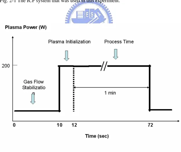
(34) Chapter 2 The Fabrication of Ultrathin 1.0 nm-thick Oxynitride Film. 2.1 The fabrication of capacitor with 1.0 nm oxynitride film In this work, Oxynitride films were grown in a parallel plate high-density plasma reactor employing an ICP source. Fig. 2-1 illustrates ICP system that was used in this experiment. 13.56 MHz RF power was coupled to the top electrode through a matching network. The substrate temperature was maintained at 300 ℃. The ultrathin oxynitride films were grown on p-type and n-type Si wafers. The silicon wafers were cleaned by the standard RCA cleaning process and dipped in a dilute HF solution (HF:H2O = 1:100) prior to loading into the chamber. The effects of system pressure, deposition time and power of plasma on the oxynitride growth rate were investigated. Fig 2-2 shows the process flow of ICP plasma oxidation process. Film thickness was determined by both the C-V and spectroscopic ellipsometry measurements. The electrical. measurements. were. conducted. on. MOS. capacitors. fabricated. lithographically by: The 500 Å polysilicon was deposited in a conventional LPCVD system at 620 ℃ with SiH4 and doped by phosphorus for heavily n+ poly gate and boron for heavily p+ poly gate ion implantation with 5 x 1015 cm-2 at 20 keV to reduce poly depletion effect. Then, the dopant was activated by RTA at 1000 ℃ for 20 sec. After activation, 50 Å Ni film was deposited by e-gun and followed by Metal RTA at 600℃ for 30 sec to form Ni silicide in order to reduce the contact resistance. Finally, a 500 nm of Al film was deposited by evaporation and MOS capacitors was patterned. The gate dielectrics of MOS capacitors with area of 10-4 cm2 were measured. Fig. 2-3 shows the process flow of ultra thin gate dielectric MOS capacitor. 18.
(35) z The detail fabrication process flow was listed as below: 1. RCA initial clean. 2. HF dip. 3. The ICP chamber was cleaned by using SiH4 and CF4 at 300 ℃ for 30 min.. 4. Different conditions was used to grow ultra thin oxynitride: (a) Different working pressure: 10, 30, 50, 100, 150 mTorr (b) Different forming gas to grow oxynitride: The working plasma will be composed by N2O, O2, or N2/O2 mixed gas at 1:1, 3:1, 5:1, and 10:1 different gas flow rate ratio. The total gas flow rate is 100 sccm. (c) Different oxynitridation time: 30 sec, 1 min,3 min,5 min,10 min for different growth time. (d) Different plasma RF power: 100 W, 200 W, 300 W, 400 W, 600 W. (e) Different nitridation time: 1 min, 3 min, 5 min, and 10 min. (f) Different forming gas to nitride oxynitride: Ar/N2 mixed gas at 9:1 and 1:9 ratio, He/N2 mixed gas at 9:1 and 1:9 ration, and N2 only.. 5. 500 Å thick poly-Si gate deposited by LPCVD at 620 ℃ in SiH4 gas.. 6.. Ion implantation: P31, 20 keV, 5 x 1015 cm-2.. 7.. Dopant activation uses furnace at 800 ℃ for 10 min and then using RTP with N2 purged at 1000 ℃ for 20 sec. 19.
(36) 8.. 50 Å thick Ni deposited by e-gun and then silicide formation by Metal RTA with N2 purged at 600 ℃ for 30 sec.. 9.. 5000 Å thick Al deposited by thermal coater for gate electrode.. 10. MOS capacitor pattern. (Al wet etch solution: H3PO4: HNO3: CH3COOH: H2O=50: 2: 10: 9) (Poly-Si wet etch solution: HNO3: H2O: NH4F =64: 33: 3). 11. HF dipped for backside native oxide remove.. 12. 5000 Å thick Al deposited by thermal coater for backside electrode.. 13. Al sintering at 360 ℃ in N2 for 20 min.. 2.2 Devices measurement method. 2.2.1 Determination of gate dielectric thickness. The thickness of gate oxide with different conditions was measured with ellipsometry immediately just after oxynitride grown. The oxide film optical parameters were measured optically using a Bean Profile Ellipsometer [1]. Ellipsometry is based on the measurement and subsequent modeling of changes in the polarization state of a light beam reflected from a sample surface, as is illustrated in Fig. 2-4. The measured parameters are the ellipsometric angles Ψ and ∆, defined from the ratio 20.
(37) R///R⊥ = tan (Ψ) exp (iΔ). (1). of the Fresnel reflection coefficients R∥ and R⊥ for the light polarized parallel and perpendicular to the plane of incidence. The reflection coefficients are determined by the optical properties and composition of the substrate and overlayers, their thicknesses, and morphology. The parameters Ψ and Δ can be measured either at a given wavelength of light, i.e., single wavelength ellipsometry, or as a function of photon energy, i.e., spectroscopic ellipsometry. The single wavelength configuration is often used for fast, nondestructive, on-line monitoring of film thickness, provided that the refractive index of the film is known. The spectroscopic mode allows determination of the refractive index as well as the thickness. For oxynitride films on Si, good agreement has been demonstrated, Fig. 2-5, between the ellipsometric oxide thickness and thickness values determined by transmission electron microscopy (TEM) and x-ray photoelectron spectroscopy (XPS), for films as thin as 2 nm [2]. Since the very first publications on Si oxidation, ellipsometry has been the tool of choice to measure film thickness. Knowledge of the thickness is critical in modeling oxidation kinetics and determining growth mechanisms [3]. The ellipsometric parameters, Ψ and Δ, can be detected with very high accuracy, making ellipsometry one of the most sensitive thickness measurement techniques. However, the interpretation of the measurements is very model dependent, especially in the ultrathin regime where refractive index may become, as is the case for SiO2, a function of thickness [4], [5]. For more complex gate dielectrics such as Si–O–N or SiO2/Si3N4 multilayer stacks, the analysis is further complicated by the fact that refractive index changes with the composition of the film [6], [7].. 21.
(38) 2.2.2 C-V and J-V measurement. The leakage current and the breakdown field strength of high-density plasma grown ultrathin oxynitride films were analyzed from the current-voltage (I-V) characteristics measured by an HP4156A semiconductor parameter analyzer. Small signal capacitance-voltage (C-V) measurements were conducted to investigate the interfacial characteristics of ultrathin oxynitride films. The C–V curves were measured by an HP 4284A precision LCR meter. The effects of the high-density plasma process on the interface state density were also analyzed. The midgap interface state density was determined by comparing high-frequency (100 k Hz) and quasi-static C–V characteristics.. . C-V measurement. The most frequently used electrical technique to assess the properties of both the thin oxide layer and its interface with Si is the C–V measurement. In thicker oxide layers C–V curves can be fitted satisfactorily with classical models, described in textbooks [8]. The C–V technique can be used to determine flatband and threshold voltage, fixed charge, and interface state density. It is also often used to determine the oxide thickness. In sub-4 nm oxide layers, C–V measurements provide the same information, but the interpretation of the data requires considerable caution. The assumptions needed to construct the ‘‘classical model’’ are no longer valid, and quantum mechanical corrections become mandatory, thus increasing the complexity of the analytical treatment. First, several authors have demonstrated that for ultrathin layers, Maxwell–Boltzman statistics no longer describe the charge density in the 22.
(39) inversion and accumulation layers satisfactorily, and should be replaced by Fermi–Dirac statistics [9]. In addition, band bending in the inversion layer near the semiconductor–insulator interface becomes very strong, and a potential well is formed by the interface barrier and the electrostatic potential in the semiconductor. This potential well may be narrow enough to give rise to electron confinement at discrete energy levels [9]. The correct analytical treatment requires solving the coupled effective mass Schrodinger and Poisson equations self-consistently. Closed form analytical treatments require a simplification of the problem [10], [11], e.g., replacing the actual potential well by a triangular well and/or by considering only the lowest subbands. One of the main effects of the quantum mechanical treatment of the inversion layer is considerable shift of the inversion charge centroid away from the semiconductor–insulator interface. This effect can be modeled as an additional capacitor in series with the oxide capacitance. A similar effect is generated by polycrystalline Si depletion on the gate side of the capacitor of a MOS transistor [12]. This effect is related to both the high fields at the insulator surface as well as the incomplete activation of the dopants near the polycrystalline Si/SiO2 interface. A carrier concentration profile with a finite width, having a centroid several tenths of a nanometer away from this interface, results. This effect can also be modeled as an additional capacitance in series with the oxide capacitance. As a consequence of quantum mechanical effects and polycrystalline Si depletion, the measured capacitance is smaller than the physical oxide capacitance, and the difference becomes very significant for ultrathin layers. This also implies that oxide thickness extraction from C–V measurements becomes more difficult, but not impossible. If C–V curves are fitted properly, a good agreement between C–V extracted oxide thickness and physical oxide thickness may be obtained [2], [9], [10]. For very thin oxides, typically sub-2 nm, the huge leakage current through the oxide, due to direct 23.
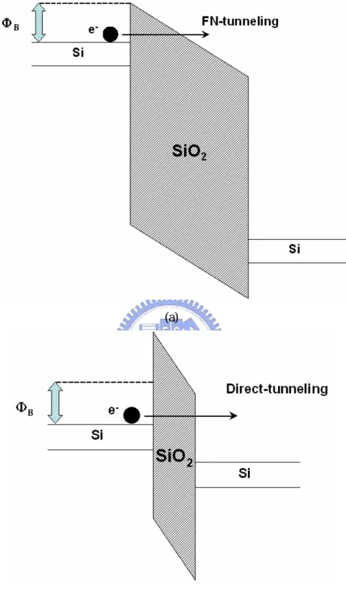
(40) tunneling of electrons, creates an additional complication in the interpretation of C–V curves. A sharp drop in the capacitance is observed as the voltage increases [13], [14]. This effect can be modeled by taking into account the tunnel conductance and an additional series resistance.. . J-V Measurement. When a voltage, Vox, is applied across an oxide layer with thickness tox, the resulting oxide field, Eox = Vox/tox, gives rise to a current flow through the oxide. This current originates from electrons that quantum mechanically tunnel through the Si/SiO2 potential barrier from the Si conduction band to the SiO2 conduction band, as is illustrated in Fig. 2-5. When the tunneling occurs through a triangular barrier, Fig. 2-6(a), the conduction mode is called Fowler–Nordheim (FN) tunneling and the measured current density, JFN. When the oxide voltage drops below 3.7 V, electrons no longer enter the oxide conduction band, but tunnel directly from the anode to the cathode, as illustrated in Fig. 2-6(b). In ultrathin oxide technologies, direct tunneling is the dominant current conduction mechanism at operating voltage, and for oxide layers less than ~3 nm it is also the conduction mode for accelerated oxide wearout and breakdown tests. The change from a FN tunneling to a direct tunneling mechanism is indicated. The huge increase due to direct tunneling poses a major leakage current problem in VLSI technologies and severely limits the scaling of the oxide thickness.. 24.
(41) 2.2.3 Determination of Reliability. . CCS and CVS. In oxides of thickness greater than 4 nm, a typical observation during high field constant current stressing (CCS) is the initial decrease of the applied voltage needed to achieve the required current, followed by a voltage increase which can become larger than the initially applied voltage [15]. The voltage shifts are caused by charge trapping of initially positive then negative charges, leading to oxide field distortion and subsequent change in the tunnel current density. During constant voltage stressing (CVS), exactly the opposite current shifts are measured, i.e., an initial increase of the current followed by a decrease.. . Stress-Induced Leakage Current (SILC). The SILC rises continuously with injected fluence, and its Vg dependence can be empirically fitted with a FN expression using a barrier height of 1 eV [16], [17]. When the SILC is continuously monitored as a function of time after a given stress, two components can be distinguished [18]. Initially, a decaying transient component is observed, leading to a steady state SILC after some time. Both components depend on oxide thickness. Thick oxides have a large transient component and low steady state component, whereas ultrathin oxides have a very small transient component and a large steady state component.. 25.
(42) . Charge to Breakdown (QBD). The E vs. 1/E model discussion is mainly valid for oxides thicker than 5 nm, where the injection of electrons is dominated by nonballistic FN injection; the injected electrons enter the conduction band of the SiO2 and interact with it. The oxide field mainly determines the electron energy at the anode and consequently, the oxide degradation. Since there exists a unique relationship between the FN current density and oxide field, QBD should be measured using CCS. For ultrathin oxides, however, the injected electrons travel ballistically through the oxide without interacting with the SiO2 network. This can be either by FN tunneling above 3.5 V, typically in oxides with thicknesses of between 5 and 3.5 nm, or by direct tunneling below 3.5 V, typically in oxides with thicknesses of below 3.5 nm. The electron energy at the anode is determined by the voltage difference between the cathode and the anode, which corresponds to the applied gate voltage [19].. 26.
(43) 2.3 References. [1]Online: http://www.thermawave.com.Therma-Wave, Inc., Fremont, CA [2]Z. H. Lu, J. P. McCaffrey, B. Brar, G. D. Wilk, R. M. Wallace, L. C. Feldman, and S. P. Tay, “SiO2 film thickness metrology by x-ray photoelectron spectroscopy,” Appl. Phys. Lett., vol. 71, pp. 2764-2766, 1990. [3]E. Irene, Solid State Mater, Crit. Rev., Sci. 14, 175, 1988. [4]K. J. Hebert, S. Zafar, E. A. Irene, R. Kuehn, J. E. McCarthy, and E. K. Demirlioglu, “Measurement of the refractive index of thin SiO2 films using tunneling current oscillations and ellipsometry,” Appl. Phys. Lett., vol. 68, pp. 266-268, 1996. [5]K. J. Hebert, T. Labayen, and E. A. Irene, The Physics and Chemistry of SiO2 and the Si-SiO2 Interface-3, edited by H. Z. Massoud, E. H. Poindexter, and C. R. Helms, Electrochemical Society, Pennington, NJ, p. 81, 1996. [6]V. A. Gritsenko, “Structure and Electronic Properties of Amorphous Insulators in Silicon MIS Structures”, Science, Novosibirsk, Russia, 1993. [7]S. C. Song, H. F. Luan, Y. Y. Chen, M. Gardner, J. Fulford, M. Allen, and D. L. Kwong, “Ultra thin (< 20 7A) CVD Si –N gate dielectric for deep-sub-micron CMOS devics,” in IEDM Tech. Dig., 1998, pp. 373–374. [8]E. H. Nicollian and J. R. Brews, MOS Physics & Technology, Wiley, New York, 1982. [9]K. S. Krisch, J. Bude, and L. Manchanda, “Gate capacitance attenuation in MOS devices with thin gate dielectrics,” IEEE Electron Device Lett., vol. 17, pp. 521-524, 1996. [10]R. Rios and N. D. Arora, “Determination of ultra-thin gate oxide thicknesses for CMOS structures using quantum effects,” in Tech. Dig. Int. Electron Devices Meet., 1994, pp. 613-616. 27.
(44) [11]C.-H. Choi, J.-S. Goo, T.-Y. Oh, Z. Yu, R. W. Dutton, A. Bayoumi, M. Cao, P. V. Voorde, D. Vook, and C. H. Diaz, “MOS C-V characterization of ultrathin gate oxide thickness (1.3-1.8 nm),” IEEE Electron Device Lett., vol. 20, pp.292-294, 1999. [12]R. Rios, N. D. Arora, and C.-L. Huang, “An analytic polysilicon depletion effect model for MOSFETs,” IEEE Electron Device Lett., vol. 15, pp. 129-131, 1994. [13]W. K. Henson, K. Z. Ahmed, E. M. Vogel, J. R. Hauser, J. J. Wortman, R. D. Venables, M. Xu, and D. Venables, “Estimating oxide thickness of tunnel oxides down to 1.4 nm using conventional capacitance-voltage measurements on MOS capacitors,” IEEE Electron Device Lett., vol. 20, pp. 179-181, 1999. [14]C.-H. Choi, J.-S. Goo, T.-Y. Oh, Z. Yu, R. Dutton, A. Bayoumi, M. Cao, P. V. Voorde, and D. Vook, “C-V and gate tunneling current characterization of ultra-thin gate oxide MOS (tox=1.3-1.8 nm),” Symp. on VLSI Tech., June, 1999, pp. 63-64. [15]D. J. DiMaria, D. Arnold, and E. Cartier, “Impact ionization and positive charge formation in silicon dioxide films on silicon,” Appl. Phys. Lett., vol.60, pp. 2118-2120, 1992. [16]J. DeBlauwe, J. V. Houdt, D. Wellekens, R. Degraeve, P. Roussel, L. Haspeslagh, L. Deferm, G. Groeseneken, and H. E. Maes, “A new quantitative model to predict SILC-related disturb characteristics in flash E2PROM devices,” in Tech. Dig. Int. Electron Devices Meet., 1996, pp. 343-346. [17]N. K. Patel and A. Toriumi, “Stress-induced leakage current in ultrathin SiO2 films,” Appl. Phys. Lett., vol. 64, pp.1809-1811, 1994. [18]R. Moazzami and C. Hu, “Stress-induced current in thin silicon dioxide films,” in Tech. Dig. Int. Electron Devices Meet., 1992, pp. 139-142. [19]J. H. Stathis and D. J. DiMaria, “Reliability projection for ultra-thin oxides at low voltage,” in Tech. Dig. Int. Electron Devices Meet., 1998, pp. 167-170. 28.
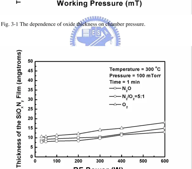
(45) Chapter 3 The Study of Ultrathin Oxynitride Grown by Using HD-ICP Plasma. 3.1 The dependence of the ultrathin oxynitride thickness. For achieving the goal of low temperature process, the temperature of all ICP plasma process was at 300 ℃. Fig. 3-1 shows the effects of the system pressure on the growth rate of oxynitride films. The oxynitride thickness was measured by optical ellipsometory. The oxynitride growth time was kept constant at 1 min. The power of working plasma was kept constant at 200 W. The system pressure was varied in the range of 10-150 mTorr. The N2O and O2 flow rate were kept constantly at 100 sccm. The N2/O2 flow rate was kept constantly at 100 and 20 sccm, respectively. The oxynitride growth rate increased from 10 mTorr to 30 mTorr but was almost uniform from 30 mTorr to 150 mTorr. The observed dependence on the system pressure suggests that growth rates of oxynitride would be stable when working at 100 mTorr. Based on the observed effect of the system pressure on the oxynitride growth rate, the high-density ICP plasma oxidation process was further investigated at a fixed system pressure of 100 mTorr. The results of oxynitride thickness versus pressure were showed at Table 3-1. Fig. 3-2 show oxynitride or oxide film thickness as a function of oxidation power for N2O, N2/O2, and O2 high-density ICP plasma at 300 ℃. The oxynitride growth time was kept constantly at 1 min. The flow rates of three kinds of gas were set as listed above. The oxidation rate of O2 plasma is faster than that of N2/O2 plasma by high-density plasma at 300 ℃. This is because of oxidation rate increases with the 29.
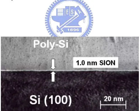
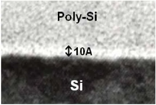
(46) increases the amount of oxygen radicals. From the same reason, the oxidation rate of O2 plasma is faster than that of N2O plasma. The oxidation rate of higher-power plasma is faster because the higher-power plasma may produce more radical to react. The results of oxynitride thickness versus power of ICP plasma were showed at Table 3-2. Fig. 3-3 shows the oxynitride thickness increased nonlinearly with time in the investigated range of 30 sec to 10 min. The power of ICP plasma was kept constantly at 200 W. The flow rates of gas were set as listed above. A rapid growth rate of oxynitride with a thickness about 10 Å was obtained after a deposition time of less than 1 min. And when the thickness of oxynitride has increased, the growth rate of oxynitride decreased. At beginning of reaction, the radical would react with surface of silicon wafer directly. After thin oxynitride films had formed, radicals must penetrate the thin oxynitride to react. So the growth rate of oxynitride was slower when the oxynitride was thicker. The results of oxynitride thickness versus oxidation time were showed at Table 3-3. Generally, the physical thickness of oxide was determined by optical elliosometer, but its accuracy cannot be guaranteed for those ultrathin films [2]. High-resolution transverse electron microscopy (HRTEM) was also performed to observe the thickness of the ultrathin oxynitride film. This method is more accurate, but still suffers from high cost and low throughput. Fig. 3-4 shows the cross section of 1.0 nm oxynitride film. The oxynitride film grown by ICP N2O plasma of 200 W for 1 min was quite uniform and the interface was smooth. Fig. 3-5 shows the enlarged HRTEM micrographs of sample grown by ICP N2O plasma of 200 W for the polysilicon-oxynitride-silicon structure.. 30.
(47) 3.2 The electrical characteristics of 1.0 nm ultrathin oxynitride films. As oxide thickness is reduced below 2.5 nm in MOS devices, both series and shut parasitic become significant in C-V measurements. The effect of increased direct tunneling current on C-V measurements can be analyzed by comparing equivalent circuit models. Conventional LCR meters typically calculate the device capacitance based on either a parallel or a series capacitance model. The leakage problem may be overcome by measuring the capacitance at a very high frequency so that the capacitive current is dominant. HP 4284A was used for high-frequency C-V measurement. We used capacitors with an area 10-4 cm2 and measurement frequency is 100 kHz. While the leakage current may be at level negligible compared with on-state current of a Si MOSFET, it will fist have an effect on the chip standby power. High-performance CMOS logic chips can tolerate a standby power in the 100mW range. If one assumes that the total active gate area per chip is of the order of 0.1 cm2 for future technologies, the maximum tolerable gate leakage current would be of the order of 1 A/cm2 for power supply of 1 V [1]. An HP 4156 semiconductor parameter analyzer and an HP 4284A LCR meter were used to measure all the relevant parameter. Small area and large area capacitors with 1.0 nm oxynitride films were used in this study.. 3.2.1 The electrical characteristics of 1.0 nm ultrathin oxynitride films grown by different power of ICP N2O Plasma. Fig. 3-6 shows the C-V curves for MOS capacitances with oxynitride by using different power of ICP N2O plasma. The oxynitride formed by using ICP N2O plasma 31.
(48) power of 200 W was the optimum condition. The maximum capacitance density could be achieved at the condition of 200 W. It had no enough energy to produce effective bonding by using lower power of ICP N2O plasma. And the effect of nitridation was not good to forming reliable gate dielectric. So the capacitance was lower and could not be maintained at high voltage. The oxynitride forming by higher power of ICP N2O plasma suffered too much plasma-induced damage, so the flatband voltage (VFB) increased. The flat band of oxynitride by ICP N2O plasma of 200 W was -0.2 V and the flat band of that of 300 W was -0.25 V. The capacitance of oxynitride by ICP N2O plasma of higher than 200 W decreased due to the increase of gate leakage current. The transitions and flat band voltages of C-V curves increased with the plasma power increased. It was the proof of that plasma-induced damage increased. Fig. 3-7 shows the I-V curves of the oxynitride by using different power of ICP N2O plasma. Clearly, the gate leakage current of oxynitride by ICP N2O plasma of 200 W was smallest. The gate leakage current of oxynitride by ICP N2O plasma of 100 W was larger because the nitrogen could not form strong bonds effectively. Thus, oxynitride by ICP N2O plasma of 100 W was similar to silicon dioxide. The nitridation effect to reduce leakage current was not good as oxynitride by ICP N2O plasma of 200 W. The gate leakage current of oxynitride by ICP N2O plasma of higher than 200 W increased due to more plasma induced damages. So the oxynitride by ICP plasma of higher power, the gate leakage current of oxynitride was larger. It had proved that the optimum condition of oxynitride was grown by ICP plasma of 200 W.. 3.2.2 The electrical characteristics of 1.0 nm ultrathin oxynitride films grown by different gas composition. The C-V characteristics of thin oxynitride grown by various composition of ICP 32.
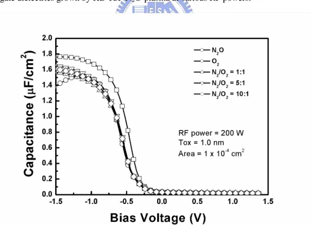
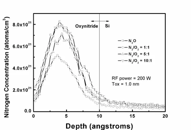
(49) plasma are shown in Fig.3-8. These oxynitride were grown by ICP plasma of 200 W at 300 ℃. The various conditions were: N2O, O2, N2/O2=1:1, N2/O2=5:1, and N2/O2=10:1, the flow rates of various condition were: 100 sccm, 100 sccm, 50 sccm:50 sccm, 100 sccm:20 sccm, and 200 sccm:20 sccm, respectively. The film grown by ICP O2 plasma was just silicon dioxide. The dielectric constant was smaller than oxynitride grown by ICP N2O plasma so the capacitance was also smaller. The capacitance of oxynitride grown by different ratio of N2 and O2 plasma were also small than that by N2O plasma. Growing oxynitride by O2 mixed N2 plasma may introduce nitrogen to dielectric, so the gate leakage current decreased and capacitance increased [2], [3]. Nitridation effect would revamp structure of oxynitride effectively [4], [5]. Appropriate ratio of N2 and O2 plasma would have better performance. Fig. 3-8 illustrate the C-V characteristics of oxynitride grown by ICP plasma of N2/O2=5:1 was better than that of N2/O2=1:1 and N2/O2=10:1. Fig 3-9 displays the I-V characteristics for thin oxynitride grown by same condition as above. It was reasonable that the gate leakage current of silicon dioxide grown by ICP O2 plasma was larger than oxynitride [6], [7]. The leakage current of the oxynitride grown by ICP plasma of various N2 and O2 plasma was smaller than that of silicon dioxide because the nitridation effect of oxynitride could decreased leakage current [8]. As results, it was sure that oxynitride grown by N2O plasma of 200 W at 1 min was the best condition.. 3.2.3 The nitrogen concentration of oxynitride grown by high-density ICP N2O plasma. Fig. 3-10 shows the nitrogen profile of oxynitride grown by different ICP plasma of 200 W. SIMS results shown in Fig. 3-10 demonstrates that the nitrogen 33.
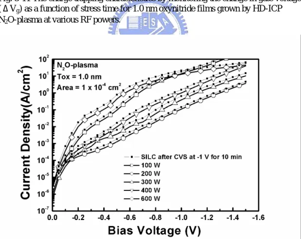
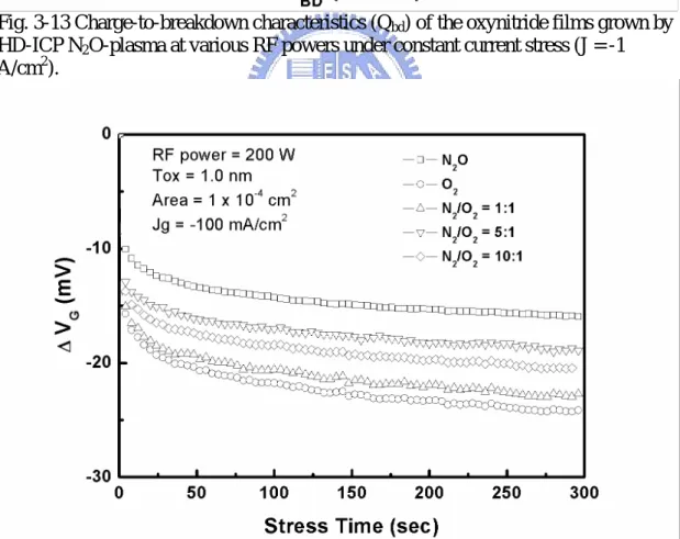
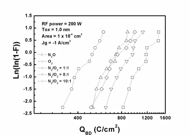
(50) concentration was low near both the interface between the dielectric and the substrate and the interface under dielectric. So for the oxynitride grown by ICP N2O plasma, the leakage current decreased and the device performance could be expected to maintain quietly [9], [10].. 3.3 The reliability of 1.0 nm ultrathin oxynitride films. After the electrical characteristics of ultrathin oxynitride grown by ICP plasma, had been verified, the reliability of ultrathin oxynitride also should need to be examined.. 3.3.1 The reliability of 1.0 nm ultrathin oxynitride films grown by different power of ICP N2O plasma. Fig. 3-11 shows the results from a constant-current stress experiment of oxynitride films that formed by using ICP N2O plasma of different power. The stress current was -100 mA/cm2. The gate voltage shift of oxynitride film formed by ICP N2O plasma of higher power was more serious. This phenomenon resulted from the plasma-induced damage. The gate voltage of oxynitride formed by N2O plasma of 100 W was larger than that by N2O plasma of 200 W because of no enough energy to produce effective bonding by using N2O plasma of 100 W. Fig. 3-12 shows the stress-induced leakage current (SILC) of oxynitride formed by ICP N2O plasma of different power. The condition of stress was on -1 V at 10 min. Charge to breakdown of oxynitride formed by N2O plasma of different power is compared in fig. 3-13. The characteristic of charge to breakdown (QBD) was measured at constant-current of -1 A/cm2. The oxynitride by using N2O plasma of 200 W also 34.
數據
+7
相關文件
Breu and Kirk- patrick [35] (see [4]) improved this by giving O(nm 2 )-time algorithms for the domination and the total domination problems and an O(n 2.376 )-time algorithm for
0 allow students sufficient time to gain confidence and the skills of studying in English, allow time for students to get through the language barrier, by going through
Students are asked to collect information (including materials from books, pamphlet from Environmental Protection Department...etc.) of the possible effects of pollution on our
By correcting for the speed of individual test takers, it is possible to reveal systematic differences between the items in a test, which were modeled by item discrimination and
The nanostructure with anisotropic transmission characteristics on ITO films induced by fs laser can be used for the alignment layer , polarizer and conducting layer in LCD cell.
1B - Time Series of the Consumer Price Index B (CPI-B) by Section 2G - Month-to-Month Change of the Composite CPI by Section 2A - Month-to-Month Change of the CPI-A by
A Boolean function described by an algebraic expression consists of binary variables, the constant 0 and 1, and the logic operation symbols.. For a given value of the binary
(Another example of close harmony is the four-bar unaccompanied vocal introduction to “Paperback Writer”, a somewhat later Beatles song.) Overall, Lennon’s and McCartney’s
