A Test and Diagnosis Methodology for RF Transceivers
Hung-kai Chen and Chauchin Su
Department of Electrical and Control Engineering
National Chiao Tung University, Hsinchu, 300, Taiwan
Abstract
This paper proposes an RF test and diagnosis methodology based on digital DFT structure and built-in DSP function of a SoC Chip. Constellation variation plots are proposed to identify the faulty component. Furthermore, linear interpolation is used to determine the amount of variation. The simulated test results show that the method is able to identify not only the faulty component but also the variation amount precise. Keywords: RF Test, RF design-for-testability, mixer, low noise amplifier, transceiver.
1. Introduction
After years of development, wireless communication has become essential for telephony and data communication. For mobile communication, there are different standards and systems in use simultaneously, such as GSM, DECT, PHS, GPRS, WCDMA, and CDMA2000. For data communication, Bluetooth, WiFi, and WiMAX fulfill different application needs. Therefore, RF circuit design and applications are wide and extensive. Due to its high added value, design houses, foundries, and system houses put a significant effort in it. In system on chip (SoC) era, embedded in a digital chip, RF circuits require special consideration in testing.
Traditionally, RF testing is achieved in two ways. The first approach is to use specialized instruments to send and receive high quality RF signals to determine the circuit parameters and go-no-go of the circuits [3, 4, 5]. The disadvantage of this approach is the cost. The instrument in RF range is not only expensive but also difficult to operate and maintain. Hence, it is difficult to meet the low cost requirement for today’s mobile hand-held devices. The second approach uses the loop back mechanism for the test [1, 2]. The digital data is sent by the transmitter and received and recovered by the receivers. It checks the bit-error rate (BER) of the received data to determine the function of the CUT. As
oppose to the former, it is low in cost, unfortunately, low in accuracy as well.
This paper proposes a test methodology that analyzes the received constellation graph to determine the parameter deviation of the active and passive components in an IF/RF transceiver. The test signal is generated by a DSP module and sent to the RF transceiver by a digital-to-analog converter (DAC). The received signal is quantized by an analog-to-digital converter (ADC) and analyzed by a DSP to determine the deviation of the components. As a result, the test overhead is minimum.
The rest of the paper is organized as follows. The test methodology and analysis are outlined in Section 2 and 3. The simulation results are presented in Section 4 and the conclusions are given in Section 5.
2. RF Transceiver and Test Methodology
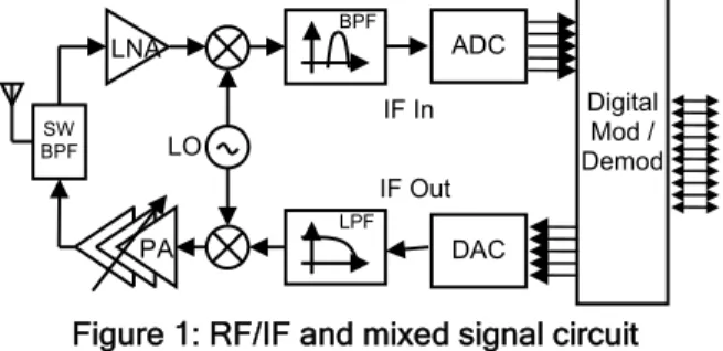
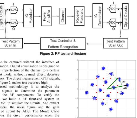
A generalized RF/IF transceiver architecture is shown in Figure 1. Digital data is modulated into digital IF signals. The signals are then converted into analog IF signals by the DAC and up converted into RF signals by the RF transmitter. The received RF signal is demodulated following a similar path in a reverse order to recover the original digital data.Figure 1: RF/IF and mixed signal circuit With digital design for testability (DFT), the digital port of DACs and ADCs are scanned as shown in Figure 2. As a results, one is able to directly control and observe digital IF signal on both ends. Therefore, one can send the IF signals to the RF module under test without distortion. Most importantly, the received
SW BPF LNA PA BPF LPF LO IF In IF Out ADC DAC Digital Mod / Demod
16th IEEE Asian Test Symposium
1081-7735/07 $25.00 © 2007 IEEE DOI 10.1109/ATS.2007.29
135
16th IEEE Asian Test Symposium
1081-7735/07 $25.00 © 2007 IEEE DOI 10.1109/ATS.2007.29
135
16th IEEE Asian Test Symposium
1081-7735/07 $25.00 © 2007 IEEE DOI 10.1109/ATS.2007.29
IF signals can be captured without the interface of digital equalization. Digital equalization is designed to overcome the imperfection of the channel to a certain degree. In test mode, without cannel effect, decrease the test accuracy. The direct measurement of IF signals, as shown in Figure 2, makes test accuracy high.
The proposed methodology is to analyze the received IF signals to determine the parameter deviation of the RF components. To verify the methodology, we build a RF front-end system in Agilent ADS tool to simulate the circuits. And extract the S-parameters, the noise figure and the gain compression of circuit by ADS. The Monte Carlo Analysis shows the circuit performance when the values of the parameters vary. Since RF performance is very sensitive to parameter deviation, small shift in parameter of a RF component may result in a dramatic change of the circuit performance. The frequency responses change along with the changes in the capacitance of the output matching network. For a particular frequency, it implies that the gain and phase are changed.
The test procedure contains four steps. First, a golden copy is selected, measured and analyzed carefully to determine its design parameters and constellation graph properties. Second, simulations are executed to determine the effects of parameter variations on the constellation graphs. Third, the constellation graph of a DUT is measured by its built-in DAC and DSP functions. Forth, the parameter variation of the DUT is analyzed by the interpolation of the measured constellation in Step 3 in the simulated results in Step 2. The interpolation can be done by a digital ATE or using the on-chip DSP function.
3. Constellation Graph Analysis
To incorporate with digitalize IF signal generation, a co-simulation environment is built in MATLAB.
Digital stimuli are generated by the baseband signal generator in MATLAB. With the known input IF signal, the frequency response shift can be obtained by the vector analysis.
For a particular RF frequency, the received constellation graph is shown in Figure 3. For which, we are able to determine the gain and phase shift
) ,
(ΔG Δθ as compared to the golden copy. The golden copy can be obtained by measuring and selecting the samples carefully. Measuring the response at different frequencies can build a three-dimensional constellation graph. The performance variation at different channels can be obtained in the additional frequency axis. According to the twist and the bend of a 3D constellation graph, we can determine the parameter shift a circuit.
4. Simulated Test Results
To analyze the constellation graphs, we compare the constellation graph to a golden copy as shown in Figure 2: RF test architecture
Figure 3: The gain variation and the phase shift of the constellation graph
136 136 136
Figure 8: The constellation variation plot for the process variation and Lout variation of the LNA Figure 3. The gain variation GΔ and the phase shift
θ
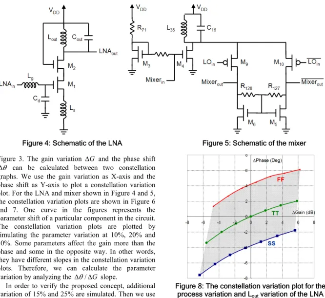
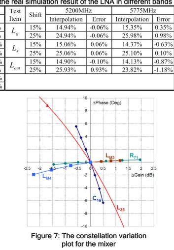
Δ can be calculated between two constellation graphs. We use the gain variation as X-axis and the phase shift as Y-axis to plot a constellation variation plot. For the LNA and mixer shown in Figure 4 and 5, the constellation variation plots are shown in Figure 6 and 7. One curve in the figures represents the parameter shift of a particular component in the circuit. The constellation variation plots are plotted by simulating the parameter variation at 10%, 20% and 30%. Some parameters affect the gain more than the phase and some in the opposite way. In other words, they have different slopes in the constellation variation plots. Therefore, we can calculate the parameter variation by analyzing the Δ /θ ΔG slope.
In order to verify the proposed concept, additional variation of 15% and 25% are simulated. Then we use linear interpolation to determine the amount of variations. The results are shown in Table 1 and Table 2. Table 1 displays the results of three channels in the lower band of 802.11a, 5160MHz, 5240 MHz and 5340MHz. For example, for a 25% change of the output capacitance C16 of the mixer at 5160MHz, the interpolation in the constellation variation plot shows that there is a 24.81% shift of C16. Table 2 displays the results of 5200MHz in the lower band and 5775 MHz in the upper band. At 5775 MHz, 15% length change of the LNA transistor M1 is tested as a 15.04% shift. The above test results show that the constellation variation plots are able to identify the component being faulty by checking the slopes of the gain and phase variations. The amount of the change can also be determined by the linear interpolation. However, there are other issues need to be considered. Process variation is the most prominent one for CMOS process.
As shown in Figure 8, process variation causes an offset in the constellation variation plots. With the test data from wafer assurance test (WAT) one is able to located the process corner. As a result, the factor of process variation can be eliminated.
5. Conclusions
In this paper we have proposed an RF test and diagnosis methodology based on digital DFT structure and built-in DSP function of a SoC Chip. Constellation variation plots are proposed to identify the faulty component. Furthermore, linear interpolation is used to determine the amount of variation. The simulated test results have demonstrated the feasibility of the proposed methodology.
Figure 4: Schematic of the LNA Figure 5: Schematic of the mixer
137 137 137
References
[1] Lupea, D.; Pursche, U.; Jentschel, H.-J., “RF-BIST: loopback spectral signature analysis,” Design, Automation and Test in Europe Conference and Exhibition, 2003, pp. 478 – 483.
[2] Heutmaker, M.S.; Le, D.K., “An architecture for self-test of a wireless communication system using sampled IQ modulation and boundary scan,” Communications Magazine, IEEE , Volume: 37 , Issue: 6 , 1999, pp. 98 – 102.
[3] Voorakaranam, R.; Cherubal, S.; Chatterjee, A., “A signature test framework for rapid production testing of RF circuits,” Proc. Design, Automation and Test in Europe Conference and Exhibition, 2002, pp. 186 – 191.
[4] Ferrario, J.; Wolf, R.; Moss, S., “Architecting millisecond test solutions for wireless phone RFICs,” Proc. Test Conference, 2002, pp. 1151 – 1158.
[5] Kasten, J.S.; Kaminska, B., “An introduction to RF testing: device, method and system,” Proc. VLSI Test Symposium, 1998, pp. 462 – 468.
[6] IEEE Std. 1057-1994, IEEE Standard for Digitizing Waveform Recorders, IEEE 1994.
Table 1: The error between the interpolation and the real simulation result of the mixer in the same band
Test
Item Shift Interpolation Error Interpolation Error Interpolation Error 5160MHz 5240MHz 5340MHz
3 M L 15% 15.05% 25% 25.07% 0.05% 0.07% 15.09% 25.14% 0.09% 0.14% 15.23% 25.23% 0.23% 0.23% 4 M L 15% 15.01% 25% 25.06% 0.01% 0.06% 15.00% 25.06% 0.00% 0.06% 14.55% 25.06% -0.45% 0.06% 16 C 15% 14.99% 25% 24.81% -0.01% -0.19% 15.00% 25.02% 0.00% 0.02% 15.11% 25.04% 0.11% 0.04% 35 L 15% 15.16% 25% 25.44% 0.16% 0.44% 15.26% 25.82% 0.26% 0.82% 15.42% 26.12% 0.42% 1.12% 71 R 15% 14.75% 25% 25.07% -0.25% 0.07% 15.04% 25.07% 0.04% 0.07% 15.06% 25.10% 0.06% 0.10%
Table 2: The error between the interpolation and the real simulation result of the LNA in different bands
Test Item Shift
5200MHz 5775MHz Test
Item Shift
5200MHz 5775MHz Interpolation Error Interpolation Error Interpolation Error Interpolation Error
1 M L 15% 14.98% -0.02% 15.04% 0.04%25% 24.99% -0.01% 25.04% 0.04% Lg 15%25% 14.94% -0.06% 15.35% 0.35%24.94% -0.06% 25.98% 0.98% 2 M L 15% 14.94% -0.06% 14.91% -0.09% Ls 15% 15.06% 0.06% 14.37% -0.63% 25% 24.94% -0.06% 24.94% -0.06% 25% 25.06% 0.06% 25.10% 0.10% d
C
15% 14.99% -0.01% 14.48% -0.52% Lout 15% 14.90% -0.10% 14.13% -0.87% 25% 24.98% -0.02% 25.30% 0.30% 25% 25.93% 0.93% 23.82% -1.18% sC
15% 25% 14.93% 24.85% -0.07% -0.15% 14.66% 24.60% -0.34%-0.40% Figure 6: The constellation variationplot for the LNA Figure 7: The constellation variation plot for the mixer
138 138 138