Broadband Microstrip-Fed Modified Quasi-Yagi Antenna
Shih-Yuan Chen and Powen Hsu Department of Electrical Engineering
and Graduate Institute of Communication Engineering National Taiwan University
Taipei 10617, Taiwan E-mail: [email protected]
A broadband design of the microstrip-fed modified quasi-Yagi antenna is presented. The two arms of the driving dipole are connected separately to two microstrip sections tapered from the feeding microstrip line and its truncated ground plane. The end points of the two tapered sections can be suitably adjusted to obtain a 10-dB return loss bandwidth more than 50%. Measured radiation patterns are end-fire and the in-band peak gains range from 3.9 to 7.2 dBi. Details of the antenna design and the experimental results are presented and discussed.
Keywords: Broadband antennas, microstrip antennas.
1. Introduction
The quasi-Yagi antenna first proposed in [1] and improved in [2] has recently become a major candidate for the waveguide transitions from planar circuit [3] and many active antenna applications, such as the spatial power-combining array [4]-[6]. The advantages of the quasi-Yagi antenna include the broadband characteristics and the good radiation performance. However, the design procedure of the quasi-Yagi antenna is somewhat bothersome as the microstrip-to-coplanar strip transition increases the design complexity enormously. In order to have similar end-fire radiation with less design parameters, a modified microstrip-fed quasi-Yagi antenna has been proposed [7]. In this paper, some modifications are made to the modified quasi-Yagi antenna to obtain a wider impedance bandwidth and simultaneously maintain satisfactory end-fire radiation patterns and antenna gains. Also, we present further information on the design and performances of the broadband modified quasi-Yagi antenna.
2. Antenna Configuration and Operation
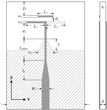
The configuration of the broadband microstrip-fed modified quasi-Yagi antenna is shown in Fig. 1. The antenna consists of an isolated microstrip as the director, a microstrip dipole as the driver, and the truncated ground plane on the backside of the substrate as the reflector. The two arms of the driving dipole are placed on the opposite sides of the substrate, one of which is fed by the strip tapered from the 50-Ω microstrip feedline, while the other is fed by the strip tapered from the truncated ground plane. Since the currents flowing on the microstrip line are out of phase with those on the ground plane, currents on the driving dipole oriented in opposite directions are in phase. In addition, the tapered line sections can guide the currents smoothly to the strip and then the driving dipole, and thus can achieve a wide impedance bandwidth. There is also an offset length Loffset (Loffset > lt) between the end points of the two tapered line sections along z-axis to mitigate the transition from the microstrip line to the two-wire line connecting the driving dipole and to further increase the impedance bandwidth. The front tapered line section which is Lt long is utilized to transform the 50-Ω microstrip feedline to a narrower line width w, while the backside tapered line section with lt long can guide the
currents from the truncated ground plane to the backside strip with the line width w. Thus, the intermediate microstrip line section that is Loffset−lt long functions as a buffer and mitigates the abrupt discontinuity. Although only the linear tapered line sections are utilized in this paper for design convenience, more complicated or higher order tapered line sections can be applied as well.
During the design process, the length of each arm of the driving dipole L2 is first determined to be a quarter guided wavelength λg/4 of the microstrip line at the required center frequency, and the length of the director L1 is chosen slightly less than λg/4. The distance between the driving dipole and the truncated ground plane d2+lt is about λg/4, and the distance between the driving dipole and the director d1 is far less than λg/4. Furthermore, the director width w1 is chosen wider than that of the driving dipole w2 for a stronger coupling to ensure a good end-fire pattern, however, this will impose a limit on the wide impedance bandwidth. Thus, compromise must be made for w1. Since the margin from the director to the substrate edge D has major influence on the return losses and hence, the impedance bandwidth, there is an optimal D for the maximum bandwidth. On the other hand, increasing the substrate width W results in a wider truncated ground plane, which is a better reflector but large in size. Consequently, there is also a trade-off for W between the antenna area and the end-fire radiation patterns.
3. Experimental Results
An X-band test piece is fabricated on the dielectric substrate Duroid 5880 with dielectric constant εr = 2.2, substrate thickness h = 1.5748 mm, and loss tangent tanδ = 0.0004. The width of the 50-Ω microstrip feedline
Wt is determined to be 5.2 mm. Design parameters in mm are as follows: D = 15.0, W = 40.0, w = 1.0, L1 = 7.4,
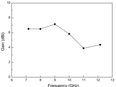
L2 = 7.5, w1 = 1.5, w2 = 1.0, d1 = 4.3, d2 = 1.2, Lt = 17.0, lt = 7.0, wt = 5.6, and Loffset = 10.0. Measured return losses of the test piece are shown in Fig. 2, in which the impedance bandwidth, defined by a return loss level of 10-dB, is 51.6% (7.17-12.16 GHz), which is much wider than 24.0% obtained in [7]. The measured in-band peak gains ranging from 7.2 to 3.9 dBi are illustrated in Fig. 3. E- and H-plane patterns measured at 8, 9, 10 and 11 GHz are shown in Figs. 4(a)-(d), respectively. In these figures, the front-to-back ratio of the end-fire patterns range from 14.0 to 20.0 dB. Since the design goal is to obtain a wider bandwidth, it is inevitable to produce a little distortion to the in-band radiation patterns. The E-plane patterns suffer from the distortion, while the H-plane patterns do not.
4. Conclusion
A broadband microstrip-fed modified quasi-Yagi antenna has been presented, implemented, and tested in X-band. This antenna simultaneously possesses a wider impedance bandwidth, satisfactory in-band peak gains, stable end-fire radiation patterns, and a compact size. By properly choosing Loffset, the impedance bandwidth can be increased to be more than 50%. In addition, the planar and simple structure makes it ease of design and mass production.
Acknowledgements
This work was supported by the National Science Council, Taiwan, R.O.C., under contract NSC 93-2752-E-002-004-PAE.
References
[1] Y. Qian, W. Deal, N. Kaneda, and T. Itoh, “Microstrip-fed quasi-Yagi antenna with broadband characteristics,” Electronics Lett., vol. 34, no. 23, pp. 2194-2196, Nov. 1998.
[2] N. Kaneda, W. Deal, R. Waterhouse, Y. Qian, and T. Itoh, “A broad-band planar quasi-Yagi antenna,”
IEEE Trans. Antenna Propagat., vol. 50, no. 8, pp. 1158-1160, Aug. 2002.
[3] N. Kaneda, Y. Qian and T. Itoh, “A broad-band microstrip-to-waveguide transition using quasi-Yagi antenna,” IEEE Trans. Microwave Theory Tech., vol. 47, no. 12, pp. 2562-2567, Dec. 1999.
[4] W. Deal, N. Kaneda, J. Sor, Y. Qian and T. Itoh, “A new quasi-Yagi antenna for planar active antenna arrays,” IEEE Trans. Microwave Theory Tech., vol. 48, no. 6, pp. 910-918, June 2000.
[5] M. Sironen, Y. Qian and T. Itoh, “A subharmonic self-oscillating mixer with integrated antenna for 60-GHz wireless applications,” IEEE Trans. Microwave Theory Tech., vol. 49, no. 3, pp. 442-450, Mar. 2001. [6] C. Hang, W. Deal, Y. Qian and T. Itoh, “High-efficiency push-pull power amplifier integrated with
quasi-Yagi antenna,” IEEE Trans. Microwave Theory Tech., vol. 49, no. 6, pp. 1155-1161, June 2001.
[7] S.-Y. Chen and P. Hsu, “A modified quasi-yagi antenna fed by a microstrip line,” in 2003 Asia-Pacific
Microwave Conference Proceedings, pp. 1741-1743.
h εr w1 L1 L2 L2 w2 w d1 d2 Lt wt lt D W Wt Loffset Y Z
Fig. 1. Geometry of broadband microstrip-fed modified quasi-Yagi antenna.
6 7 8 9 10 11 12 13 -20 -15 -10 -5 0 |S 11 | ( dB ) Frequency (GHz)
6 7 8 9 10 11 12 13 0 2 4 6 8 10 Gain (dBi ) Frequency (GHz)
Fig. 3. Measured peak antenna gains of the prototype antenna.
-30 -20 -10 0 30 60 90 120 150 180 210 240 270 300 330 E-plane H-plane -30 -20 -10 0 30 60 90 120 150 180 210 240 270 300 330 E-plane H-plane (a) (b) -30 -20 -10 0 30 60 90 120 150 180 210 240 270 300 330 E-plane H-plane -30 -20 -10 0 30 60 90 120 150 180 210 240 270 300 330 E-plane H-plane (c) (d) Fig. 4. Radiation patterns of the prototype antenna measured at (a) 8.0, (b) 9.0, (c) 10.0, and (d) 11.0 GHz.