References
I Proc. SPIE: Imaging Technologies and Applications. Vol. 1778. 1992
2 GUPTA. M.M., and KNOPF, G.K. (Ed.): “euro-vision systems, principles and applications’ (IEEE Press, 1994)
3 DELEROCK, T.: ‘Silicon retina with correlation-based, velocity tuned pixels’, IEEE Trans., 1993, “4, (3), pp. 529-541
4 SOCLOF, s.: ‘Applications of analog integrated circuits’ (Prentice Hall Inc., 1985)
5 VIDAL.M.P, B A F L E U K M , ~uxo,~., and SARRABAYROURE,G.: ‘A bipolar photodetector compatible with standard CMOS technology’, So/id State Ekcfron., 1991, 34, (S), pp. 809-814
HUERTAS. I.L., and SANCHEZ-SINENCIO, E.: ‘An analog design technique for smart-pixel CMOS chips’. Proc. 1993 ESSCIRC, September 1993, (Sevilla), pp. 78-81
6 ESPEJO. S., RODRIGUEZ-VAZQUEZ, A., DOMINGUEZ-CASTRO, R.,
Low voltage BiCMOS dynamic logic gates
H.P.
Chen and Y.P. Wu
Indexing terms: BiCMOS integrated circuits, Logic gates
A low-supply-voltage BiCMOS logic gate is presented which can be used to form a pipelined system using the two-phase non- overlapping clocks. The new BiCMOS dynamic logic gates have no DC power dissipations and they have full voltage swings. It has been shown that the use of the described feedback technique provides a lower gate delay than previously reported low-voltage designs.
Introduction: Performance degradation at low voltage is verified to be a major limiting factor for BiCMOS circuits. The reduced swing degrades the speed of the driven gates, especially when the supply voltage is scaled down. Another disadvantage of the reduced swing is the noise margin reduction. To overcome the drawback, full-swing complementary designs using complementary bipolar device have been recently reported [I]. However, the advantages of the C-BiCMOS are considerably offset by the addi- tional process complexity and cost for the pnp bipolar fabrication. In this Letter, a circuit technique using a feedback inverter to improve the BiCMOS logic swing and allow low voltage operation is proposed. This design offers an effective speed improvement over other existing designs, such as merged BiCMOS (M-BiC- MOS) [2] and quasi-complementary BiCMOS (QC-BiCMOS) 131, without using extra processing steps in an npn-only BiCMOS process.
t
K J
qQ’
M N I*
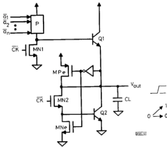
Fig. 1 Proposed BiCMOS dynamic N-ceN
L
0
f ’
4 0*
Fig. 2 Proposed BiCMOS dynamic P-ceN
Circuit: The full-swing operation can be realised by using a feed- back inverter as shown in Figs. 1 and 2. To organise to form a dynamic pipelined system [4], the logic gates can be divided into two types, the N-cell and P-cell. The operation of these two gates is as follows. As shown in Fig. 1, the N-cell has two operation phases, that is, precharge phase and evaluation phase. During the precharge period when the CK signal is low, MN1 is turned off, and the current supplied by M P l is fully used to drive Ql. The output node is charged quickly to a value higher than V, - VBE.
Using the feedback inverter, the output node is pulled up to V , through MPe. After the precharge period when the CK signal goes high, MNe is turned off and the base of Ql is discharged through MN1. Hence, short circuit current in Ql and Q2 can be avoided during the next pull-down thereby reducing unnecessary power dissipation. The output logic value is determined by the logic cir- cuit block N, which is composed of nMOS transistors. Assuming a high-to-low transition at the output node due to the logic value, the output voltage decreases until it reaches VBE. MNe is turned on in this time. This could lead to the saturation of Q2 causing the output voltage to fall to V,,, close to OV. As shown in Fig. 2, the operation of the P-cell can be similarly explained as follows. Dur- ing the predischarge phase when is high, Q l is turned off due to the turned on MN1 and the output node is discharged to set up to low level, close to 0 V. During the evaluation phase when is low, MN1 is turned off and the base of Q2 is discharged by MNe. The output logic value is determined by the logic circuit block P, which is composed of PMOS transistors
0 1 0 20 30
ns mm
Fig. 3 Transient waveforms of the four inverters
- -
0- -
CMOS_____ M-BiCMOS [I]
.... QC-BiCMOS [2]
- -
0- -
proposed BiCMOS (N-cell+ P-cell)
Comparisons: To compare the performance of the proposed BiC- MOS circuit with those of CMOS, M-BiCMOS, and QC-BiCMOS circuits, the series of two inverters of each BiCMOS circuit is sim-
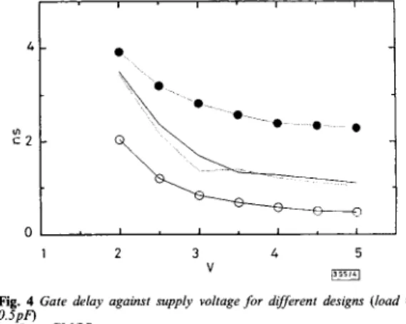
dated. The MOS device threshold voltages are -fo.7V. Fig. 3 shows the simulated transient waveforms of those logic gates (with 0.5pF load). As indicated in the Figure, the gate delay time of the proposed BiCMOS circuit is 2.21ns, which means the response speed of the proposed circuit is more than three times that of a CMOS inverter (7.111s). The proposed BiCMOS circuit can also be seen to provide a faster response speed than the other two BiC- MOS designs. Fig. 4 shows the simulated dependence of the gate delay on Vdd for those four equal area inverters (with 0.5pF load). The proposed BiCMOS circuit is almost 160% faster than a CMOS circuit at 3V and also considerably faster than other npn- only BiCMOS logic gates.
I
I
”0 1 ” ” ” ’ ~ 1
1 2 3 4 5
v
a
Fig. 4 Gate delay against supply voltage for different designs (load =
- -
0- -
CMOS~ M-BiCMOS [l]
-... QC-BiCMOS [2]
- -
0- -
proposed BiCMOS0 . 5 ~ 0
Application: As shown in Fig. 5, the N-cell and P-cell are replaced alternatively in the BiCMOS dynamic CLA circuit.
P,
and G, are the carry propagation and carry generation, respectively. After the prechargeipredischarge phase, each output node is set high andlow in the dynamic circuit alternatively, such that the output node of the N-celliP-cell turns off the pMOSinMOS in the next stage and the output node of each stage is not affected by the previous carry signal. During the evaluation phase, the output node of each stage is determined by the logic circuit. Thus, it is realised that the new dynamic BiCMOS circuit is fully racefree. The two types of cells should be connected alternatively in a system, thus forming an extensively pipelined structure. In fact, the arrangement of N-
celllP-cell can be used in any large-scale pipelined dynamic system to shorten the propagation delay time associated with complex irregular routing [5].
CK
CK :
CK :
Fig. 5 Example application of proposed dynamic logic gate
Conclusion: A novel BiCMOS dynamic logic gate is presented, which is suitable for organisation in a pipelined system. Without special IC processing, the new BiCMOS dynamic logic gates enhance the speed performance over other types of low voltage npn-only BiCMOS designs. Even at 2V, it is 100% faster than a CMOS design (with 0.5pF load). The proposed BiCMOS logic gates provide an absolute speed advantage, which is very helpful for low-supply-voltage operation.
0 IEE 1994
Electronics Letters Online No: 19941263
H. P. Chen and Y. P. Wu (Rm. 319, Dept. of Electrical Eng., National Tainm University #I. Roosevelt Rd., Sec. 4, Taipei 106-17, Taiwan)
BEG
-
22 August 1994
References
SHIN, H.I., CHEN. C.-L., JOHNSON, E.D., TAUR, Y., RAMASWAMY, S., and BOUDON, G.: ‘Full-swing complementary BiCMOS logic circuits’,
BCTM, 1989, 138, (l), pp. 229-232 @p. 83-90, 1991)
RITTS, R.B., RAIE, P.A., PLUMMER, J.D., SARASWAT, K.C., and CHAM, K.M.: ‘Merged BiCMOS logic to extend the CMOS/BiCMOS performance crossover below 2.5V supply’, IEEE J. Solid-State Circuits, 1991, SC-26, pp. 1606-1614
NISHIDA, R., SEKI, K., and SHIMOHIGASHI, K . : ‘Quasi-complementary BiCMOS for sub-3-V digital circuits’, IEEE J. Solid-State Circuits,
1991, SC-26, pp. 1708-1719
GONCALVES, N.F., and DEMAN, H.1.: ‘NORA: A racefree dynamic CMOS technique for pipeline logic structures’, IEEE J. Solid State Circuits, 1983, SC-18, (3), pp. 261-266
CHEN, H.P., LIAO, H.J., and KUO, J.B.: ‘BiCMOS dynamic full adder circuit for high-speed parallel multipliers’, Electron. Lett., 1992, 28, (12), pp. 1124-1126
YANO. K., HIRAKI. M., SHUKURI, S., ONOSE, Y., HIRAO, M., OHKI, N . ,
Deep high-dose erbium implantation
of
low-
loss
silicon oxynitride waveguides
A.V. Chelnokov, J.-M. Lourtioz, Ph. Boucaud,
H. Bemas, J. Chaumont and
T.
Plowman
Indexing terms: Oprical waveguides, Ion implantation, Photoluminescence
Photoluminescence studies of low-loss SiON waveguides deeply (2.8MeV) implanted with erbium at concentrations up to latm.% are reported. Rapid thermal annealing at 900°C is found to repair most of the implantation damage and results in a 5.3111s ‘Illi2 lifetime for 0.25atm.% Er concentration. Measurements in 1 atm.% doped samples show significant erbium ion-ion interactions.
Introduction: A strong demand exists for active silicon-based opto- electronic devices, such as amplifiers, zero-loss splitters and so on, due to their technological compatibility with available silicon elec- tronics. Silicon oxynitride (SON) could be among the promising materials for such devices. Recently, very low-loss optical SiON waveguides have been made by plasma-enhanced chemical vapour deposition (PECVD) on 4 inch wafers [I]. The optical index of SiON can be vaned from that of SiO, (i.e. n = 1.46) to almost that of Si,N, (n = 2.2) by changing the portion of nitrogen in the compound during growth. Thus, optical waveguide mode size can be controlled without changing the waveguide geometry. Unfortu- nately, no results on rare-earth doping of SiON in order to obtain optical amplification have been published to date. From this view- point, ion implantation appears to be a useful investigation tech- nique because it allows the incorporation of erbium ions, among others, in virtually any solid host material [2, 31. Moreover, the Er concentration profile can be easily controlled while the maximum concentration can exceed the limit of solubility.
In this Letter, we report for the first time on the photolumines- cent characteristics of low-loss SiON waveguides heavily doped with Er by using deep ion implantation.
Experimental setup: A standard 100 mm diameter silicon wafer with a 3 p n layer of thermally grown SiO, was used as a substrate. A 1 . 1 8 ~ thick SiO,,N,, guiding layer was deposited using PECVD. Losses as low as O.OSdB/cm were measured at 633nm for 7cm long waveguides. One optical mode was supported at both 0 . 9 8 ~ and 1 S p n wavelengths. No transverse optical confine- ment structure was realised on the samples.
The waveguides were implanted with 2.8MeV Er ions at room temperature. The implantation energy was chosen to provide max- imum erbium concentration at a depth of 0 . 6 4 . 7 ~ ~ the latter corresponding to the position of the maximum of the 0 . 9 8 ~ pump mode spatial distribution. Two implantation doses were used: 5 x 10¹⁵cn-2 and 2 x 10’6cn-2, which resulted in -0.25atm.Yo and -1 .Oatm.”h peak Er ions Concentrations, respectively.
Thereafter, the implanted waveguides were repeatedly annealed