phys. stat. sol. (a) 204, No. 6, 1977–1981 (2007) / DOI 10.1002/pssa.200674711
Paper
Hybrid nitride microcavity using crack-free highly reflective
AlN/GaN and Ta
2O
5/SiO
2distributed Bragg mirrors
G. S. Huang*, 1, Hou-Guang Chen2, J.-R. Chen1, T. C. Lu1, H. C. Kuo1, and S. C. Wang1 1 Department of Photonics & Institute of Electro-Optical Engineering, National Chiao Tung University,
1001 Ta Hsueh Road, Hsinchu, 300 Taiwan
2 Department of Materials Science and Engineering, I-Shou University, Kaohsiung County, 840 Taiwan Received 9 September 2006, revised 21 December 2006, accepted 26 December 2006
Published online 15 May 2007
PACS 42.55.Sa, 42.79.Fm, 68.37.Lp, 78.55.Cr, 78.66.Fd, 81.15.Gh
We report the growth over 2 inch sapphire substrates of hybrid nitride-based microcavities using one crack-free highly reflective AlN/GaN distributed Bragg reflectors (DBRs) incorporated with AlN/GaN superlattice (SL) insertion layers and Ta2O5/SiO2 DBRs. The optical cavity is formed by a 5λ cavity con-sisting of n-type GaN, 10 pairs multiple quantum wells and p-type GaN sandwiched by AlN/GaN and Ta2O5/SiO2 DBRs. Reflectivity and photoluminescence measurements were carried out on these struc-tures. A 29 periods AlN/GaN DBR incorporated with six AlN/GaN superlattice insertion layers showed no observable cracks and achieved a peak reflectivity of 99.4% and a stopband of 21 nm. Based on these high quality DBRs, the cavity mode is clearly resolved with a linewidth of 2.6 nm. These results demon-strate that the AlN/GaN system is very promising for the achievement of strong light – matter interaction and the fabrication of nitride-based vertical cavity surface emitting lasers.
© 2007 WILEY-VCH Verlag GmbH & Co. KGaA, Weinheim
1 Introduction
The fabrication of high quality nitride microcavities (MC) has recently attracted much attention both for fundamental studies and technological applications. MCs can indeed be used to improve the extraction efficiency of light and to obtain a more directional emission from light emitting diodes [1 – 4]. Further-more, MCs with high reflectivity mirrors are required to achieve strong coupling between excitons and cavity photons [5] or to fabricate vertical cavity surface emitting lasers [3, 6, 7]. In addition, the III-nitride semiconductor materials have much larger oscillator strength and binding energy of excitons than other conventional III – V compound semiconductor materials, making them as excellent candidates for observing the strong coupling regime toward room temperature (RT) and understanding of polariton physics. Potential applications of strong coupling in high quality GaN microcavity would be the fabrica-tion of polariton lasers operating at a significantly lower threshold current than convenfabrica-tional nitride la-sers as well as nonlinear optical devices like micro-optical parametric amplifiers and ultrafast switches [8 – 10].
One approach of high-quality nitride-based MCs have previously been reported using at least one dielectric mirror because of the difficulty to grow high reflectivity nitride distributed Bragg reflectors (DBRs) [5 – 7]. The commonly used DBR material system, AlxGa1−xN/GaN, requires at least 20 – 60 per-iods depending on the Al content to achieve reflectivity values exceeding 99%. Another approach has been recently proposed, using lattice-matched Al0.82In0.18N/GaN DBRs [11]. With this lattice-matched
reflectivity of 97% was demonstrated. In this paper, we further report the growth over 2 inch sapphire substrates of hybrid type nitride-based microcavities using one crack-free highly reflective AlN/GaN DBR with superlattice insertion layers and Ta2O5/SiO2 distributed Bragg reflectors. The optical cavity is formed by a 5λ cavity consisting of n-type GaN, 10 pairs multiple quantum wells and p-type GaN sand-wiched by AlN/GaN and Ta2O5/SiO2 DBRs.
2 Experiments
These samples were grown in a low pressure EMCORE D75 MOCVD system. Two-inch diameter (0001)-oriented sapphire substrates were used for the growth of samples. Trimethylgallium and trimethy-laluminum were used as group III source materials and ammonia as the group V source material. After thermal cleaning of the substrate in hydrogen ambient for 5 min at 1100 °C, a 30 nm-thick GaN nuclea-tion layer was grown at 500 °C. The growth temperature was raised up to 1100 °C for the growth of 2 µm GaN buffer layer. Then AlN/GaN DBR with AlN/GaN SL insertions was grown under the fixed chamber pressure of 100 Torr similar to the previous reported growth conditions [12]. Then n-type GaN and following by a ten pairs InGaN/GaN (2.5 nm/10 nm) multiple quantum wells and p-type GaN were grown to form a 5λ cavity. Finally, an eight pairs of Ta2O5/SiO2 dielectric mirror was deposited by elec-tronic beam evaporation as the top DBR reflector. The reflectivity spectra of the GaN/AlN DBRs and the full microcavity structure were measured by the n & k ultraviolet – visible spectrometer with normal inci-dence at room temperature. The thicknesses of the individual layers in the DBRs were investigated by transmission electronic microscopy (TEM). The photoluminescence (PL) emission was excited by a 325 nm He – Cd laser of 30 mW and dispersed by a 0.32 m monochromator and detected with a pho-tomultiplier with standard lock-in technique.
3 Results and discussion
Room temperature reflectivity spectra of crack free DBR measured near normal incidence are presented in Fig. 1. We have previously reported the 20 pairs of crack free AlN/GaN DBR with three superlattices
400 420 440 460 480 500 0 20 40 60 80 100 98.3% DBR1 99.4% DBR2 R e flec tivi ty (% ) Wavelength (nm) 440 480 520 0 20 40 60 80 100 R e flecti vity (% ) Wavelength (nm) A B C A B C
Fig. 1 Reflectivity spectra of two AlN/GaN DBRs with peak reflectance of 98.3% and 99.4% at centre wave-lengths of 434 and 461 nm, respectively.
Fig. 2 Reflectivity spectra of the DBR 2 taken across the 2 inch wafer, which are located in order from the center of the wafer to the edge along the radius.
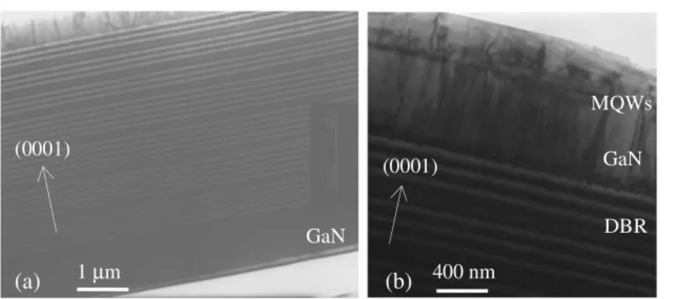
phys. stat. sol. (a) 204, No. 6 (2007) 1979 Paper (a) 1µm (b) (0001) DBR GaN MQWs GaN 400 nm (0001)
Fig. 3 (a) TEM cross-sectional images of 29 pairs AlN/GaN DBRs incorporated with 6 pairs insertion layers, (b) 5λ cavity and DBRs.
insertion layers achieving peak reflectivity of 97% at 399 nm with stopband of 14 nm [12]. The sample labeled DBR 1 was 25 pairs of crack free AlN/GaN DBR with four superlattice insertion layers. One pair of AlN/GaN superlattice insertion layers, which was the same as our previous report [12], was inserted between each five pairs of AlN/GaN DBRs. Here we define the stopband between the reflectivity more than 97%. The peak reflectivity of 98.3% at 434 nm with stopband of 19 nm was shown in Fig. 1. In order to achieve crack free and the higher reflectivity DBR, the sample was 29 pairs of AlN/GaN DBRs with six insertion layers. We chose to insert one superlattices layer in the first four sets of five pairs of DBR and second three sets of three pairs of DBR. The sample labeled DBR 2 shows the peak reflectivity of 99.4% at 461 nm with stopband of 21 nm. The flat topped stopband and the well-defined oscillations in particular the short wavelength ones most sensitive to internal absorption effects are indicative of the high sample quality. Figure 2 shows the reflectance spectra of DBR 2 at three areas A, B and C, which are located in order from the center of the wafer to the edge along the radius. At area A, the peak reflec-tivity of 98% was obtained at wavelength of 460 nm, at area B, 99.4% at 461 nm, and at area C, 95% at 465 nm, respectively. The difference of peak wavelength was 5 nm across the wafer.
The cross-sectional TEM image of DBR 2 is shown in Fig. 3(a), where the entire DBR 2 structure can be observed. The lighter layers represent AlN while the darker layers represent GaN or AlN/GaN super-lattice insertion layer. From the bottom to the up, the AlN/GaN supersuper-lattice layer was inserted between each five pairs of DBR, then each three pairs of DBR consequently. It is interesting to note the uniform-ity of the thickness across the entire structure. In Fig. 3(a), no cracks can be observed in the TEM image. However, some V-shaped defects (dark spots) were still observed on the interfaces of GaN or AlN layers in Fig. 3(a). These V-shaped defects have been reported earlier to be due to various origins such as stack-
350 400 450 500 550 0 2000 4000 6000 0 20 40 60 80 100 Intensity (a.u.) Wavelength (nm) 2.6 nm R e flectivity (% )
Fig. 4 Room temperature reflectivity and PL spectra of 5λ cavity mode.
Typical room temperature reflectivity spectrum measured on this hybrid microcavity consisting of 29 pairs of AlN/GaN DBRs incorporated with AlN/GaN superlattices insertion layers and 8 pairs of Ta2O5/SiO2 DBRs is presented in Fig. 4. The large stopband (70 nm) results from the significant refrac-tive index contrast between Ta2O5 and SiO2 layers. The cavity dip mode is measured at 454 nm corre-sponding to the emission peak. However, the full width at half maximum (FWHM) of the dip is 8 nm due to the bad resolution of spectrum. Figure 4 shows the PL spectrum from the microcavity at room temperature. The cavity resonance mode at 454 nm with a FWHM of 2.6 nm is clearly observed as shown in Fig. 4. It indicates the emission peak is well aligned with vertical cavity formed by the high reflectance of AlN/GaN DBR with superlattices insertion layers and Ta2O5/SiO2 DBR. The cavity quality
factor is of the order of 175. This value is lower than the theoretical value of 1050 that calculated from the reflectivities of both AlN/GaN and Ta2O5/SiO2 DBRs. The lower Q-factor is partly due to the absorp-tion of InGaN/GaN quantum wells and p-type GaN inside the cavity. Carlin et al. [4] reported an empty 3λ/2 GaN cavity surrounded by AlInN/GaN DBRs with reflectivities close to 99%. The Q-factor of our sample is nearly same as that of their sample (180). Furthermore, we inserted a 5λ cavity consisting of n-type GaN, 10 pairs multiple quantum wells and p-type GaN instead of their no light emitter inside GaN cavity.
4 Conclusions
In summary, using the AlN/GaN system incorporated with superlattice insertion layers, Bragg mirrors with reflectivity higher than 99.4% were obtained. The fabrication of hybrid nitride-based microcavities made of crack-free highly reflective AlN/GaN DBRs and dielectric mirror was demonstrated. Their char-acteristic linewidth of the cavity mode of 2.6 nm and stopband width of 21 nm corresponding to the state-of-the-art for nitride MCs are comparable to those achieved in nitride based MCs. In particular, the Q-factor of 175 could be promising for the demonstration of strong light – matter interaction in hybrid MCs at room temperature. This should pave the way toward the fabrication of optoelectronics devices like VCSELs and polariton based lasers.
Acknowledgements This work was supported by the MOE ATU program and in part by the National Science Council of Republic of China (ROC) in Taiwan under contract No. NSC 95-2120-M-009-008 and No. NSC 94-2215-E-009-082.
References
[1] E. F. Schubert, Y. H. Wang, A. Y. Cho, L. W. Tu, and G. J. Zydzik, Appl. Phys. Lett. 60, 921 (1992).
[2] M. Diagne, Y. He, H. Zhou, E. Makarona, A. V. Nurmikko, J. Han, K. E. Waldrip, J. J. Figiel, T. Takeuchi, and M. Krames, Appl. Phys. Lett. 79, 3720 (2001).
[3] Chih-Chiang Kao, Y. C. Peng, H. H. Yao, J. Y. Tsai, Y. H. Chang, J. T. Chu, H. W. Huang, T. T. Kao, T. C. Lu, H. C. Kuo, S. C. Wang, and C. F. Lin, Appl. Phys. Lett. 87, 081105 (2005).
[4] J.-F. Carlin, J. Dorsaz, E. Feltin, R. Butté, N. Grandjean, M. Ilegems, and M. Laügt, Appl. Phys. Lett. 86, 031107 (2005).
[5] T. Tawara, H. Gotoh, T. Akasaka, N. Kobayashi, and T. Saitoh, Phys. Rev. Lett. 92, 256402 (2004). [6] T. Someya, R. Werner, A. Forchel, M. Catalano, R. Cingolani, and Y. Arakawa, Science 285, 1905 (1999). [7] I. L. Krestnikov, W. V. Lundin, A. V. Sakharov, V. A. Semenov, A. S. Usikov, A. F. Tsatsul’nikov, Zh. I.
Alferov, N. N. Ledentsov, A. F. Hoffmann, and D. Bimberg, Appl. Phys. Lett. 75, 1192 (1999).
[8] G. Malpuech, A. di Carlo, A. V. Kavokin, J. J. Baumberg, A. Zamfirescu, and P. Lugli, Appl. Phys. Lett. 81, 412 (2002).
phys. stat. sol. (a) 204, No. 6 (2007) 1981
Paper
[9] P. G. Savvidis, J. J. Baumberg, R. M. Stevenson, M. S. Skolnick, D. M. Whittaker, and J. S. Roberts, Phys. Rev. Lett. 84, 1547 (2000).
[10] M. Saba, C. Ciuti, J. Bloch, V. Thierry-Mieg, R. André, Le SiDang, S. Kundermann, A. Mura, G. Bongiovanni, J. L. Staehli, and B. Deveaud, Nature (London) 414, 731 (2001).
[11] J.-F. Carlin and M. Ilegems, Appl. Phys. Lett. 83, 668 (2003).
[12] G. S. Huang, T. C. Lu, H. H. Yao, H. C. Kuo, S. C. Wang, Chih-Wei Lin, and Li Chang, Appl. Phys. Lett. 88, 061904 (2006).
[13] H. M. Ng, D. Doppalapudi, E. Iliopoulos, and T. D. Moustakas, Appl. Phys. Lett. 74, 1036 (1999). [14] H. M. Ng, T. D. Moustakas, and S. N. G. Chu, Appl. Phys. Lett. 76, 2818 (2000).