This content has been downloaded from IOPscience. Please scroll down to see the full text.
Download details:
IP Address: 140.113.38.11
This content was downloaded on 25/04/2014 at 16:59
Please note that terms and conditions apply.
Improvement of light output in GaN-based power chip light-emitting diodes with a nano-rough
surface by nanoimprint lithography
View the table of contents for this issue, or go to the journal homepage for more 2008 Semicond. Sci. Technol. 23 045022
(http://iopscience.iop.org/0268-1242/23/4/045022)
Semicond. Sci. Technol. 23 (2008) 045022 (4pp) doi:10.1088/0268-1242/23/4/045022
Improvement of light output in
GaN-based power chip light-emitting
diodes with a nano-rough surface by
nanoimprint lithography
H W Huang
1,2, C H Lin
2, C C Yu
2, B D Lee
2, C H Chiu
1, C F Lai
1,
H C Kuo
1, K M Leung
3, T C Lu
1and S C Wang
11Institute of Electro-Optical Engineering, National Chiao Tung University, Hsinchu 30050, Taiwan,
Republic of China
2Mesophotonics Limited, Hsinchu 300, Taiwan, Republic of China
3Department of Computer and Information Science, Polytechnic University, Six Metrotech Center,
Brooklyn, NY 11201, USA
E-mail:[email protected]
Received 10 January 2008, in final form 16 February 2008 Published 20 March 2008
Online atstacks.iop.org/SST/23/045022
Abstract
The enhancement of light extraction of gallium nitride (GaN)-based power chip (PC)
light-emitting diodes (LEDs) with a p-GaN rough surface by nanoimprint lithography (NIL) is presented. At a driving current of 350 mA and a chip size of 1 mm× 1 mm, the light output power of the PC LEDs with a p-GaN rough surface (etching depth from 130 to 150 nm) showed an enhancement of 24% on wafer when compared with the same device without NIL. Current–voltage results indicated an ohmic contact by the increase in the contact area of the nano-roughened surface at 200 mA. This paper offers a promising potential for enhancing the output powers of commercial LEDs.
(Some figures in this article are in colour only in the electronic version)
1. Introduction
Recently, the development in high-brightness gallium nitride (GaN)-based light-emitting diodes (LEDs) being implanted in flat-panel displays has made more possible for the LEDs to be used in many display technologies [1, 2]. To further reduce the cost and enhance the performance of these LEDs, there is always a great need to improve the internal as well as external quantum efficiency in order to further increase their light output power. Furthermore, the external quantum efficiency of GaN-based LEDs is low because the refractive index of the nitride epitaxial layer differs greatly from that of the air. The refractive indices of GaN and air are 2.5 and 1.0, respectively. Thus, the critical angle at which light generated in the InGaN/GaN-active region can escape is approximately [θc = sin−1(nair/nGaN) ] ∼23◦, which limits the external
quantum efficiency of conventional GaN-based LEDs to only a
few percent [3]. The light from LEDs can be enhanced either through the sample surface or through the sidewalls of the chip. Research into improving the light extraction efficiency (external quantum efficiency) and brightness in the LEDs [3–8] has been intense. Recently, we reported an increase in the extraction efficiency of GaN-based LEDs by surface roughening [7, 8]. All these processes allow the photons generated within the LEDs to find the escape cone, by multiple scattering from a rough surface.
The insertion of a nano-rough pattern that can control the propagation of photons has become more important. To fabricate the nanosized pattern, e-beam lithography (EBL) [9, 10], laser interference lithography (LIL) [11] and nanoimprint lithography (NIL) [12, 13] have been used. However, EBL and LIL techniques have a low throughput and cannot be applied for the mass production of LED devices. Compared with EBL and LIL, NIL is one of the
Semicond. Sci. Technol. 23 (2008) 045022 H W Huang et al
SiO2depo sition
Pol ymer coatin g
Mold Heat an d pr essure
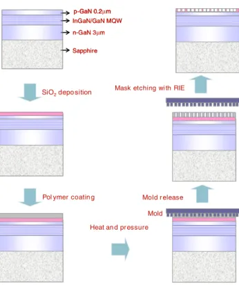
Mold r elease Mask etching wi th RIE InGaN/GaN MQW p-GaN 0.2 m n-GaN 3 m Sapphire InGaN/GaN MQW p-GaN 0.2 m p-GaN 0.2µm n-GaN 3µm Sapphire
Figure 1. Process flow schematic diagram for nanoimprint
lithography.
most promising technologies for nanosized pattern fabrication due to its high resolution and high throughput patterning capability with an extremely low cost for developing LED devices [13]. This investigation reports the production of GaN-based LEDs with a nano-roughened surface by NIL. As a result, the light output efficiency of an LED with a nano-roughened surface (etching depth from 130 to 170 nm) was significantly higher than that of a conventional LED without a roughened surface. Additionally, the current–voltage (I–V) measurements demonstrate that the forward voltage of an LED with a nano-roughened surface was lower than that of a conventional LED at 200 mA from the same wafer with standard device processing.
2. Experiments
GaN-based LED samples were grown by metal-organic chemical vapor deposition (MOCVD) with a rotating-disk reactor (Emcore D75TM) on a c-axis sapphire (0001) substrate
at a growth pressure of 200 mbar. The LED structure consists of a 50 nm thick GaN nucleation layer grown at 500 ◦C, then a 2 µm undoped GaN buffer layer grown at 1050 ◦C, a 3 µm thick Si-doped GaN layer grown at 1050 ◦C, an unintentionally doped InGaN/GaN multiple quantum well (MQW) active region grown at 770◦C, a 50 nm thick Mg-doped p-AlGaN electron-blocking layer grown at 1050 ◦C, a 0.2 µm thick Mg-doped p-GaN contact layer grown at 1050◦C. The MQW active region consists of five periods of 3 nm/7 nm thick In0.15Ga0.85N/GaN quantum well layers and
barrier layers. Figure1is a detailed process flow schematic
Figure 2. The etching rate of the p-GaN layer as a function of the
ICP-RIE etching time.
diagram for our NIL. Firstly, the 50 nm SiO2was deposited
onto the sample surface by plasma-enhanced chemical vapor deposition (PECVD). Secondly, we spin-coated a polymer layer on top of the SiO2. Thirdly, we placed a patterned
mold onto the dried polymer film. By applying high pressure, we heated the LED samples to above the glass transition temperature of the polymer. Fourthly, the LED samples and the mold were then cooled down to room temperature to release the mold. Finally, we used reactive-ion etching (RIE) with CF4
plasma to remove the residual polymer layer and transferred the pattern onto SiO2.
By inductively coupled plasma RIE (ICP-RIE), we partially etched the p-GaN surfaces of the LED samples using Cl2/Ar as the etching gas. The etching gases Cl2 and Ar
were introduced into the reactor chamber through independent electronic mass flow controllers (MFCs) that could control the flow rate of each gas with an accuracy of about 1 sccm (standard cubic centimeters per minute). An automatic pressure controller (APC) was placed near the exhaust end of the chamber to control the chamber pressure. Figure2shows the etching rate of the p-GaN layer as a function of ICP-RIE etching time. The etching rate of the p-GaN layer using the ICP etching condition, Cl2/Ar= 10/25 sccm with the ICP source power, bias power set at 200/200 W and chamber pressure of 2.5 mTorr, was determined to be approximately 7.5 nm s−1. The etching depth increased from 80 to 235 nm with the increasing etching time from 15 to 30 s. The ICP etching process for PC LEDs was used to form rough surface with four different etching times (LED I: 18 s, LED II: 20 s, LED III: 22 s and LED IV: 25 s). We then used a buffer oxidation etchant (BOE) to remove the residual SiO2layer.
Afterward, the conventional LED and the LED with a nano-rough surface by NIL were fabricated using the standard process (three mask steps) with a mesa area (950× 950 µm2). Firstly, the 0.52 µm SiO
2was deposited onto the
sample surface by PECVD. Photo lithography was used to define the mesa pattern after wet etching of SiO2by a BOE
solution. The mesa etching was then performed with Cl2/Ar
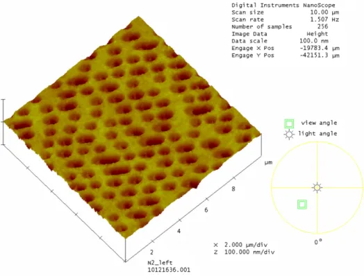
Figure 3. The AFM image of LEDs by nanoimprint lithography without the RIE etching process.
as the etching gas in an ICP-RIE system transferred the mesa pattern onto the n-GaN layer. A 300 nm thick ITO layer was subsequently evaporated onto the LED samples surface. The ITO layer had a high electrical conductivity and a high transparency. The metal pad layers were patterned by a lift-off procedure and deposited onto samples by electron beam evaporation. Cr/Pt/Au (20/30/1000 nm) were used for the p- and n-type electrode. For comparison, PC LEDs with and without a p-GaN nano-rough surface by NIL were chosen from the same wafer location possessing the same internal quantum efficiency and the same emitting wavelength.
Figure3shows the AFM pattern image of PC LEDs with a nano-rough surface by NIL without RIE etching. The AFM image shows that the nano-hole dimension and the density of the PC LEDs mesa surface were approximately 200–500 nm and 1× 108cm−2, respectively, and the polymer layer height
was approximately 0.15 µm. 3. Results and discussion
The light output was detected by a calibrated integrating sphere with a Si photodiode on the LED wafer device. Figure 4
shows the typical I–V characteristics. It was found that the measured forward voltages at an injection current of 350 mA at room temperature for the conventional LED, LED I, LED II, LED III and LED IV were 4.56, 4.58, 4.62, 4.66 and 2.76 V, respectively. In figure 4, the I–V results indicated that nano-roughening facilitates p-type contact, resulting in an ohmic contact by the increase in the contact area of the nano-roughened surface below 200 mA (because of the better ohmic contact with the nano-roughened surface in the current range
0 100 200 300 400 500 0 2 4 6 Forwar d current (mA) Voltage (V) 0 6 6
Figure 4. Current–voltage (I–V) measurement characteristics of PC
LEDs with a nano-rough surface by nanoimprint lithography and conventional LEDs, respectively.
from 10 to 200 mA). However, over 300 mA the nano-rough surface by NIL indicated that there is heating and charging damages for the fabrication process of NIL during the ICP etching process. Further, the forward voltage of LED IV is lower as the etching depth of the p-AlGaN layer induces the leakage current.
The intensity–current (L–I) characteristics of the five different types of LEDs are shown in figure5. We clearly observed that the output powers of the LED I (etching
Semicond. Sci. Technol. 23 (2008) 045022 H W Huang et al 0 100 200 300 400 500 0.0 5.0x10⁻³ 1.0x10⁻² 1.5x10⁻² 2.0x10⁻² 2.5x10⁻² 3.0x10⁻² 3.5x10⁻² Li ght out p ut i n te nsi ty ( a rb. uni ts ) Current ( mA ) Conventional LED
LED I (Etching depth=130nm) LED II (Etching depth=150nm) LED III (Etching depth=170nm) LED IV (Etching depth=195nm)
No output power
Figure 5. Intensity–current (L–I) characteristics of PC LEDs with a
nano-rough surface by nanoimprint lithography and conventional LEDs, respectively.
depth= 130 nm) and LED II (etching depth = 150 nm) were larger than that of the conventional LEDs. At an injection current of 350 mA, the light output power of the PC LEDs with a nano-rough surface by NIL on wafer shows enhancement by 24% compared to the PC conventional LEDs. The 24% improvement in the light emission reported here compares very well with the 25% improvement reported by Cho et al [14] This enhancement is attributed to the higher scattering effect of PC LEDs with a nano-rough surface by NIL (etching depth from 130 to 150 nm) when compared to conventional LEDs.
4. Conclusion
In conclusion, GaN-based PC LEDs with a nano-rough surface by NIL were demonstrated and fabricated. At a driving current of 350 mA and a chip size of 1 mm × 1 mm, the light output power of PC LEDs with a nano-rough surface by NIL showed an enhancement of 24% when compared with conventional LEDs. I–V properties indicated that nano-roughening facilitates p-type contact, resulting in an ohmic contact by the increase in the contact area of the nano-roughened surface below 200 mA.
Acknowledgments
The authors would like to thank Professor S Y Kuo of Chang Gung University for technical support. This work
was supported by the National Science Council NSC94-2752-E009-007-PAE, NSC94-2120-M009-007, Republic of China. References
[1] Schubert E F 2003 Light-Emitting Diodes (Cambridge: Cambridge University Press)
[2] Koike M, Shibata N, Kato H and Takahashi Y 2002 Development of high efficiency GaN-based
multi-quantum-well LEDs and their applications IEEE J.
Select. Top. Quantum Electron.8 271
[3] Huh C, Lee K S, Kang E J and Park S J 2003 Improved light-output and electrical performance of InGaN-based light-emitting diode by microroughening of the p-GaN surface J. Appl. Phys.93 9383
[4] Fujii T, Gao Y, Sharma R, Hu E L, DenBaars S P and Nakamura S 2004 Increase in the extraction efficiency of GaN-based light-emitting diodes via surface roughening
Appl. Phys. Lett.84 855
[5] Oder T N, Shakya J, Lin J Y and Jiang H X 2003 III-nitride photonic crystals Appl. Phys. Lett.83 1231
[6] Oder T N, Kim K H, Lin J Y and Jiang H X 2004 III-nitride blue and ultraviolet photonic crystal light emitting diodes
Appl. Phys. Lett.84 466
[7] Huang H W, Chu J T, Kao C C, Hsueh T H, Yu C C, Kuo H C and Wang S C 2005 Enhanced light output of an
InGaN/GaN light emitting diode with a nano-roughened p-GaN surface Nanotechnology16 1844
[8] Huang H W, Kuo H C, Chu J T, Lai C F, Kao C C, Lu T C, Wang S C, Tsai R J, Yu C C and Lin C F 2006
Nitride-based LEDs with nano-scale textured sidewalls using natural lithography Nanotechnology17 2998
[9] David A, Fujii T, Moran B, Nakamura S, DenBaars S P, Weisbush C and Benisty H 2006 Photonic crystal laser lift-off GaN light-emitting diodes Appl. Phys. Lett.
88 133514
[10] Lai C F, Kuo H C, Chao C H, Hsueh H T, Wang J F T, Yeh W Y and Chi J Y 2007 Anisotropy of light extraction from two-dimensional photonic crystal light-emitting diodes Appl. Phys. Lett.91 123117
[11] Divliansky I B, Shishido A, Khoo I C, Mayera T S, Pena D, Nishimura S, Keating C D and Mallouk T E 2001 Fabrication of two-dimensional photonic crystals using interference lithography and electrodeposition of CdSe
Appl. Phys. Lett.79 3392
[12] Byeon K J, Hwang S Y and Lee H 2007 Fabrication of two-dimensional photonic crystal patterns on GaN-based light-emitting diodes using thermally curable
monomer-based nanoimprint lithography Appl. Phys. Lett.
91 091106
[13] Chang S J, Shen C F, Chen W S, Kuo C T, Ko T K, Shei S C and Sheu J K 2007 Nitride-based light emitting diodes with indium tin oxide electrode patterned by imprint lithography
Appl. Phys. Lett.91 013504
[14] Cho H K et al 2006 Light extraction enhancement from nano-imprinted photonic crystal GaN-based blue light emitting diodes Opt. Express14 8654