Field emission and photofluorescent characteristics of zinc oxide nanowires
synthesized by a metal catalyzed vapor-liquid-solid process
Seu Yi Li, Pang Lin, Chia Ying Lee, and Tseung Yuen Tseng
Citation: Journal of Applied Physics 95, 3711 (2004); doi: 10.1063/1.1655685 View online: http://dx.doi.org/10.1063/1.1655685
View Table of Contents: http://scitation.aip.org/content/aip/journal/jap/95/7?ver=pdfcov
Published by the AIP Publishing
Articles you may be interested in
On the origin of enhanced photoconduction and photoluminescence from Au and Ti nanoparticles decorated aligned ZnO nanowire heterostructures
J. Appl. Phys. 110, 124317 (2011); 10.1063/1.3671023
Enhanced field emission from ZnO nanowires grown on a silicon nanoporous pillar array
J. Appl. Phys. 108, 114301 (2010); 10.1063/1.3516156
Raman and photoluminescence properties of highly Cu doped ZnO nanowires fabricated by vapor-liquid-solid process
J. Chem. Phys. 129, 124713 (2008); 10.1063/1.2981050
Effect of phosphorus dopant on photoluminescence and field-emission characteristics of Mg 0.1 Zn 0.9 O nanowires
J. Appl. Phys. 99, 024303 (2006); 10.1063/1.2161420
Field emission of zinc oxide nanowires grown on carbon cloth
Appl. Phys. Lett. 85, 1407 (2004); 10.1063/1.1784543
Field emission and photofluorescent characteristics of zinc oxide
nanowires synthesized by a metal catalyzed vapor-liquid-solid process
Seu Yi Li and Pang Lin
Institute of Materials Science and Engineering, National Chiao Tung University, Hsinchu, Taiwan, 30049, Republic of China
Chia Ying Lee and Tseung Yuen Tsenga)
Department of Electronics Engineering and Institute of Electronics, National Chiao Tung University, Hsinchu, Taiwan, 30050, Republic of China
共Received 19 May 2003; accepted 13 January 2004兲
The ZnO nanowires synthesized by vapor-liquid-solid growth mechanism with Cu and Au as the catalyst were investigated. The principal differences in morphology between Cu and Au catalyzed ZnO nanowires are observed and lead to significant differences in their field emission and photofluorescent characteristics. The Cu catalyzed ZnO nanowires with a high-quality wurtzite structure were grown vertically on p-type Si共100兲 substrate along 关0002兴 direction. A strong ultraviolet emission at 381 nm is observed. These ZnO nanowires show excellent field emission properties with turn-on field of 0.83 V/m and corresponding current density of 25A/cm2. The emitted current density of the ZnO nanowires is 1.52 mA/cm2at a bias field of 8.5 V/m. The large field emission area factor, arising from the morphology of the nanowire field emitter, is partly responsible for the good emission characteristics. The ZnO nanowires with high emission current density and low turn-on field are expected to be used in field emission flat panel display. © 2004 American Institute of Physics. 关DOI: 10.1063/1.1655685兴
I. INTRODUCTION
Since carbon nanotubes 共CNTs兲 were discovered in 1991,1 the worldwide nanotechnology research has been quite extensive on one-dimensional 共1D兲 nanostructures, such as CNTs, oxide nanobelts 共or nano ribbons兲,2 and nanowires.3– 6These fascinating structures have drawn much attention because of their interesting growth mechanisms, physical properties, and applications in the electro-optical nanodevices.7–11 Optical explorations of these nano-structured materials are focused on the field emission and photoluminescence共PL兲 characteristics. In general, there are three nanowire growth mechanisms: vapor-liquid-solid
共VLS兲 growth mechanism,12
metalorganic vapor phase epi-taxy deposition,13 and template method.14 Among these growth mechanisms, the metal catalytic VLS growth mecha-nism provides a cheap process for large-area deposition of nanowire array. ZnO, a direct band gap共3.37 eV兲 semicon-ductor with exciton binding energy of 60 meV, is a suitable material for optical application. Several previous studies have shown that ZnO nanowires exhibit strong UV laser emission, which can be used in luminescent device applications.15–18 In our study, the ZnO nanowires are syn-thesized by the VLS process with Cu19 and Au as the cata-lysts in Ar atmosphere on p-type Si共100兲 substrate. The mor-phology, structural, composition, photoluminescence, and field emission characterizations of these nanowires were ex-amined.
II. EXPERIMENT
Before the VLS process, a Radio Corporation of America method was used to clean p-type Si共100兲 substrate and put the substrate in ultrasonic bath of acetone for 30 min. This process can remove the native oxide from the surface of Si substrate. After the cleaning procedure, thin films of Au and Cu were deposited on Si共100兲 substrate by rf sputtering
共13.56 MHz兲 under 10 mTorr Ar atmosphere using 30 W for
15 s. The thicknesses of Cu and Au thin films were about 70–100 Å. This metal layer acts as a catalyst for ZnO nano-wire growth.
The ZnO nanowires were synthesized by VLS process12 with temperature in the range of 750–950 °C. A quartz boat was filled with a mixture of ZnO and graphite powder and loaded in a horizontal quartz tube furnace with an inner di-ameter of 7.62 cm. A precisely controlling carrying gas flow pattern共CGFP兲 method was employed to control the growth process of ZnO nanowires. For such CGFP method, the car-rier gas outlet was put into the center of the horizontal fur-nace and was below the quartz boat about 0.5 cm. The dis-tance between gas outlet and the center of quartz boat was about 75 cm. The rate of increase in temperature was 150 °C/ min under high purity Ar共99.998%兲 atmosphere with the gas flow rate from 20.0 to 100.0 cm3/s. Besides, we also used general VLS method for the preparation of some Au cata-lyzed ZnO nanowires for which the gas outlet was located above the quartz boat and other growth conditions were the same as the CGFP method. These two different gas con-trolled methods were employed to study the effect of synthe-sis on the structure and property of the ZnO nanowires. In a separate experiment, the Si substrate with metal film was put
a兲Author to whom correspondence should be addressed; electronic mail:
3711
0021-8979/2004/95(7)/3711/6/$22.00 © 2004 American Institute of Physics
in the furnace with the same heating procedures as the VLS process we used. The appearance of such Si substrate surface before VLS growth was observed by atomic force micros-copy共AFM, Digital Instrument兲. The crystal structure of the nanowires was studied by x-ray diffraction共XRD, MAC Sci-ence, MXP18, Japan兲. The morphology of the ZnO nanow-ires was analyzed by field emission scanning electron mi-croscopy 共FE-SEM, Hitachi S-4700I, Japan兲 and high resolution transmission electron microscopy共HRTEM, Phil-ips tecani-20兲. The chemical composition of the ZnO nanow-ires was characterized by Auger electron microprobe 共AES, VG Scientific Microlab 350, UK兲. A photoluminescence ana-lyzer共PL, Hitachi F-4500, Japan兲 with Xe lamp as an exci-tation source 共320 nm兲 was used for optical studies at room temperature.
For field emission characteristic, an indium tin oxide glass 共16 ⍀/䊐, RiTEK Co., Taiwan兲 anode was placed at a distance of 320m from a tip of ZnO nanowires. A Keithley 237 source-measure unit was used for measuring the current–voltage (I – V) and field emission characteristics. Field emission measurements were carried out in a vacuum chamber with a pressure of 1⫻10⫺5 Torr at room tempera-ture.
III. RESULTS AND DISCUSSION
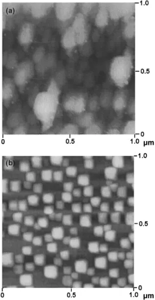
Figure 1 shows that the surface morphology of Si sub-strate with Au thin film after heating process is an irregular island structure. However, the surface configuration of Si substrate with Cu thin film is an ordered square or hexagonal island structure. The different surface morphology of catalyst film will affect the distribution of the ZnO nanowires on the Si substrate, which will be described in a later section.
Figure 2 shows the proposed VLS growth mechanism of ZnO nanowires. There are at least four different stages in-volved in the formation of ZnO nanowires: metal thin film deposition, catalytic nanoparticle formation, nucleation of ZnO and epitaxial growth of ZnO nanowires. In this experi-ment, the Cu and Au form the nanosized metal droplets.
As the temperature is increased to the reaction tempera-ture, the ZnO was reduced by graphite and CO(g). The cor-responding chemical reaction can be expressed as follows:
ZnO共s兲⫹C共s兲→Zn共g兲⫹CO共g兲, 共1兲 CO共g兲⫹ZnO共s兲→CO2共g兲⫹Zn共g兲. 共2兲 The gaseous products produced by reactions共1兲 and 共2兲 would adsorb and condense on the catalytic droplets. Subse-quently, the following reaction共3兲 is catalyzed by the metal droplets at solid–liquid interface
Zn共g兲⫹CO共g兲→ZnO共s兲⫹C共s兲, 共3兲 C共s兲⫹CO2共g兲→2CO共g兲. 共4兲
As the substrate temperature decreases, the metal drop-lets form the spherical caps in front of the ZnO nanowires. Sometimes these droplets will be burnt away for the longer time VLS process. The substrate surface indicated a light or dark gray color after reaction.
The SEM photographs 关Figs. 3共a兲 and 3共b兲兴 show the
microstructure of the ZnO nanowires synthesized with Au and Cu by CGFP method. Figure 3共a兲 illustrates the mor-phology of the ZnO nanowires grown with Au as the cata-lyst. Randomly distributed hexagonal pillars exist on the Si substrate. The lengths of these nanowires are ⬃5 m and diameters are in the range from 20 to 30 nm. The morphol-ogy of the nanowires synthesized with Cu as the catalyst is shown in Fig. 3共b兲. The ZnO nanowires are well aligned on the Si substrate with a length of 5 m and diameter of 50 nm. But the morphology of Cu catalyzed ZnO nanowires is quite different from that of Au catalyzed nanowires. This is due to the different liquefaction temperature of the catalytic metal. As the temperature rises in the VLS process, Au–Si alloy droplet formed rapidly on the Si substrate because of the low eutectic point 共360 °C兲20 of the Au–Si alloy. There-fore, the surface of the Au film is the larger irregular island structure and the orientation of Si substrate affects the growth direction of the ZnO nanowires. When the Cu is em-ployed in the VLS process, Cu–Si alloy droplets are hard to
FIG. 1. AFM images of the共a兲 Au and 共b兲 Cu thin film surface after heating process.
3712 J. Appl. Phys., Vol. 95, No. 7, 1 April 2004 Liet al.
form on the surface for the high eutectic point 共802 °C兲20of Cu–Si alloy. The surface of the Cu catalyst film has many ordered square and hexagonal Cu island structures and the lattice parameter of Cu (a⫽3.215 Å) is close to that of the
ZnO (a⫽3.253 Å). Consequently, the ZnO nanowires can vertically grow from Cu layer on the Si substrate with CGFP method.
The XRD patterns of ZnO nanowires synthesized with Au and Cu as the catalysts are shown in Fig. 4. As seen in the Fig. 4共a兲, there exist weak diffraction peaks identified as
共100兲 and 共002兲 of the ZnO nanowires synthesized with Au
as the catalyst, which is attributed to the random and disor-dered distribution of the ZnO nanowires dispersed on the Si substrate 关Fig. 3共a兲兴. When the CGFP method was adopted, the ZnO nanowires had higher共002兲 peak intensity. Further-more, the ZnO nanowires also have excellent preferred共002兲 orientation of Fig. 4共c兲 when replacing the catalyst from Au to Cu by the CGFP method. The appearance of well crystal-lized and vertically directed nanowires was also demon-strated on a SEM photograph in Fig. 3共b兲.
The HRTEM image of Cu-catalyst nanowires shown in Fig. 5 indicates the lattice fringes along 关0002兴 direction of the ZnO nanowires. The spacing of the lattice fringes along the c axis of the ZnO nanowire is⬃5.21 Å, which is
identi-FIG. 2. Schematic illustration of VLS nanowire growth mechanism 共a兲 metal film deposition,共b兲 metal nanoparticles formation, 共c兲 absorption and nucleation,共d兲 epitaxial growth.
FIG. 3. FE-SEM photographs for共a兲 Au and 共b兲 Cu catalyzed ZnO nanow-ires synthesized on p-type Si共100兲 substrate with adopting CGFP method.
FIG. 4. XRD patterns of ZnO nanowires synthesized with共a兲 Au as the catalyst,共b兲 Au as the catalyst by CGFP method, and 共c兲 Cu as the catalyst by CGFP method.
FIG. 5. HRTEM image of Cu catalyzed ZnO nanowires. The selected area electron diffraction共SAED兲 pattern is shown in inset 共a兲, while bright view image for sidewall of the ZnO nanowires, is indicated in inset共b兲.
cal to the recorded pattern in International Centre for Dif-fraction Data–Joint Committee on Powder DifDif-fraction Stan-dards No. 80-0075 of ZnO bulk material. The selected area electron diffraction 共SAED兲 pattern is shown in the inset of Fig. 5共a兲. The direct beam is along 共200兲, and the diffraction pattern of the ZnO nanowire reveals that this nanostructure is single crystalline. After diffraction pattern analysis, the in-dexed zone axis 共002兲, 共020兲, 共022兲 can be labeled. The re-sult demonstrated that the Cu catalyst-assisted fabrication of ZnO nanowires leads to perfect wurtzite 共hcp兲 crystalline structure. In Fig. 5共b兲, the bright view image showed the smooth sharp sidewall of the ZnO nanowires, which also proved the CGFP method is helpful in controlling the mor-phology of the ZnO nanowires.
Figure 6 depicts the AES spectrum of the ZnO nanow-ires, indicating that the chemical compositions of the ZnO nanowires have two major elements, Zn and O, and one mi-nor contaminant, C. Three strong intense signals of Zn are located at 833, 913, and 991 eV; two signals of O are located at 488 and 510 eV. The weak C signal peak at 273 eV is derived from the carbothermal route adopted for the synthe-sis of the ZnO nanowires. After noise calibration and inte-grated calculation, the Zn and O atomic ratio is around 1:1 which is identical with transmission electron microscopy-energy dispersive spectroscopy analysis result.
Figure 7共a兲 depicts the photoluminescence 共PL兲 spectra at room temperature of the ZnO nanowires which were syn-thesized with Cu, and Au as catalysts by the CGFP method, and with Au as the catalyst without the CGFP method, re-spectively. According to the figure, a strong UV emission
共⬃381 nm兲 and weak green emission 共⬃501–570 nm兲 are
observed in the PL spectrum of the ZnO nanowires synthe-sized with Cu as the catalyst under the control of CGFP method. The strong UV emission 共⬃381 nm兲 is due to the near band edge emission of the wide band gap of ZnO, while the weak intensity of green emission共⬃501–570 nm兲 is as-cribed to the singly ionized oxygen vacancies in ZnO.21 Therefore, we can suggest that there should be a few oxygen
vacancies in these ZnO nanowires that are synthesized with Cu as the catalyst under the control of the CGFP method. It is easy to perceive the contrast between the PL spectra of ZnO nanowires synthesized with Cu and Au as the catalysts. That is, a little wavelength shift, from 381 to 368 nm, exists in the spectra of the shorter length 共3 m兲 and randomly distributed nanowires synthesized with Au as the catalyst. This is because of the rare catalyst materials, such as Cu and Au, which diffuse in the ZnO nanowires and serve as the recombination centers. In order to realize the relationship between the impurities and the optical characteristics, the absorption coefficient measurement was taken, and the opti-cal band gap of the ZnO nanowires was opti-calculated by Tauc’s22 plot关Fig. 7共b兲兴. By the Tauc22 equation, the optical band gap (Eg) can be determined from the intercept of
(␣h)1/2vs h plot, where␣is the absorption coefficient, h is the Planck constant, andis the frequency of radiation. As shown in Fig. 7共b兲, the Tauc plot provides an estimate of the optical band gaps of these ZnO nanowires. Of those, the ZnO
FIG. 6. Typical AES spectrum of Cu catalyzed ZnO nanowires.
FIG. 7. 共a兲 PL spectra of the ZnO nanowires grown on the p-type Si sub-strate.共b兲 Tauc’s plot of the ZnO nanowires grown on the p-type Si sub-strate.
3714 J. Appl. Phys., Vol. 95, No. 7, 1 April 2004 Liet al.
nanowires, which were synthesized with Cu as the catalyst by the CGFP method, have the smallest optical band gap with 3.24 eV. The Au catalyzed ZnO nanowires without adopting the CGFP method have a 3.45 eV optical band gap. The largest optical band gap is obtained for the ZnO nanow-ires synthesized with Au as the catalyst by the CGFP method, having 3.52 eV. It is known that the shorter optical band gap is responsible for the longer emitted wavelength. On the other hand, the impurities which incorporate in the ZnO nanowires cause the various optical band gaps and the UV band emission properties. In addition, the randomly distrib-uted ZnO nanowires synthesized with Au as the catalyst without using the CGFP method have the weak UV emission intensity. It implies that the disordered distribution of the ZnO nanowires decreases the UV emission ability of the ZnO nanowires.
Figure 8 displays the field emission I – V plots for the well-aligned and randomly grown ZnO nanowire array using different metal catalysts. The I – V characteristics of ZnO nanowires grown with different metal catalysts 共Fig. 3兲 fol-lowed a Fowler–Nordheim 共FN兲23–25 behavior, which is shown in the inset of Fig. 8 where ln(I2/V) is plotted as a function of 104/V 共FN plot兲 and characterized by three con-stant slopes of FN plots of Cu and Au catalyzed nanowires using the CGFP method and Au catalyzed nanowires without adopting the CGFP method, respectively. When the work function of the nanowires is known, the field emission area factorcan be obtained from the slope of FN plot. The work function for the ZnO nanowire has been reported to be 5.37 eV.23–25Thevalue of Cu catalyzed ZnO nanowires is about 7.18⫻103. The other  values of Au catalyzed with and without adopting the CGFP method are 4.70⫻103 and 3.81
⫻103, respectively. The  value of the Cu catalyzed ZnO
nanowires is the bigger than those catalyzed by Au, that is, the Cu catalyzed ZnO nanowires display much larger effi-cient emission area than Au catalyzed nanowires. The field
emission area factor  usually depends on the geometry, structure, tip size and number densities of the ZnO ires grown on the substrate. Our Cu catalyzed ZnO nanow-ires exhibit higher value 共that is, larger field emission ef-ficiency兲 than other reported ZnO nanowires26(⫽847) and CNTs27 (⫽1.1⫻103) mainly because of their vertical growth, better crystalline structure共Fig. 4兲 and lower density
共Fig. 3兲. On the other hand, the field-adjustment factor ␣, which is an index, determined the ability to enhance local field from the field emission tips. In our experiment,␣values are 1.21⫻10⫺5, 0.92⫻10⫺5 and 0.88⫻10⫺5 for Cu cata-lyzed ZnO nanowires and Au catacata-lyzed ZnO nanowires with and without adopting the CGFP method, respectively. This result indicates that␣value for Cu catalyzed ZnO nanowires is larger than those of Au catalyzed ZnO nanowires, which means that vertical growth tips of the ZnO nanowires have better ability to enhance local field.
On the basis of Fig. 8, the turn-on field of Cu catalyzed ZnO nanowires is 0.82 V/m at current density of 25.0
A/cm2. The emission current density is 1.5 mA/cm2 at an applied field of 8.5 V/m. The turn-on fields and correspond-ing current densities for Au catalyzed ZnO nanowires with and without adopting the CGFP method are 0.92 V/m, 13.0
A/cm2and 0.97 V/m, 12.7A/cm2, respectively. Our Cu catalyzed ZnO nanowires exhibit lower turn-on voltage and higher emission current densities than the ZnO nanowires synthesized by Lee’s research group,26which were about 6.0 V/m and emission current density of 1.0 mA/cm2at a bias field of 11.0 V/m, respectively. These results illustrate that the ZnO nanowire array is sufficient for flat panel field emis-sion display applications in the future.
IV. CONCLUSIONS
In summary, well-aligned and vertically grown Cu cata-lyzed ZnO nanowires, which have an excellent wurtzite structure, less contamination and precise chemical composi-tion, were successfully grown at 750–950 °C by adopting a CGFP method. The ZnO nanowires emitted strong UV at
⬃381 nm at room temperature by using Xe lamp 共320 nm兲 as
the excitation source. The field emission measurements indi-cated high emission current density of 1.5 mA/cm2under the field of 8.5 V/m and low turn-on field of 0.83 V/m at current density of 25A/cm. The Cu catalyzed ZnO nanow-ires exhibited a higher field emission area factor of about 7.18⫻103 and a larger field adjustment factor of 1.21
⫻10⫺5 than those values of Au catalyzed nanowires, which
is due to the vertical direction growth of Cu catalyzed nanowires. Such a vertically grown ZnO nanowire array is a good candidate for the future flat panel display applications.
ACKNOWLEDGMENT
This work was supported by the National Science Coun-cil of ROC under Contract No. NSC 92-2216-E009-022.
1S. Iijima, Nature共London兲 354, 56 共1991兲.
2J. Zhang and L. Zhang, Chem. Phys. Lett. 363, 293共2002兲. 3
C. Wang, M. Chen, G. Zhu, and Z. Lin, J. Colloid Interface Sci. 243, 362 共2001兲.
4A. Fert and L. Piraux, J. Magn. Magn. Mater. 200, 358共1999兲.
FIG. 8. Field emission characteristics of the ZnO nanowires grown on
p-type Si substrates. The inset reveals the FN plots of the ZnO nanowires.
5C. C. Tang, S. S. Fan, M. Lamy de la Chapelle, and P. Li, Chem. Phys.
Lett. 333, 12共2001兲.
6N. Wang, Y. F. Zhang, Y. H. Tang, C. S. Lee, and S. T. Lee, Phys. Rev. B 58, 16024共1998兲.
7D. M. Bagnall, Y. F. Chen, Z. Zhu, T. Yao, S. Koyama, M. Y. Shen, and T.
Goto, Appl. Phys. Lett. 70, 2230共1997兲.
8
M. T. Bjo¨rk, B. J. Ohlsson, T. Sass, A. I. Persson, C. Thelander, M. H. Magnusson, K. Deppert, L. R. Wallenberg, and L. Samuelson, Appl. Phys. Lett. 80, 1058共2002兲.
9M. H. Huang, S. Mao, H. Feick, H. Yan, Y. Wu, H. Kind, E. Weber, R.
Russo, and P. Yang, Science 292, 1897共2001兲.
10Y. S. Lee and T. Y. Tseng, J. Mater. Sci. Materi. Electron. 9, 65共1998兲. 11Y. W. Wang, L. D. Zhang, G. Z. Wang, X. S. Peng, Z. Q. Chu, and C. H.
Liang, J. Cryst. Growth 234, 171共2002兲.
12M. Huang, S. Mao, H. Feick, H. Yan, Y. Wu, H. Kind, E. Weber, R. Russo,
and P. Yang, Science 292, 2242共2001兲.
13Y. Wu, R. Fan, and P. Yang, Int. J. Nanosci. 1, 1共2002兲.
14Y. Li, G. W. Meng, L. D. Zhang, and F. Phillip, Appl. Phys. Lett. 76, 2011 共2000兲.
15
J. S. Leea, M. I. Kanga, S. Kima, M. S. Leeb, and Y. K. Lee, J. Cryst. Growth 249, 201共2003兲.
16K. Park, J. S. Lee, M. Y. Sung, and S. Kim, Jpn. J. Appl. Phys., Part 1 41,
7317共2002兲.
17Y. K. Tseng, I. N. Lin, K. S. Liu, T. S. Lin, and I. C. Chen, J. Mater. Res. 18, 714共2003兲.
18H. T. Ng, B. Chen, J. Li, J. Han, M. Meyappan, J. Wu, S. X. Li, and E. E.
Haller, Appl. Phys. Lett. 82, 2023共2003兲.
19S. Y. Li, C. Y. Lee, and T. Y. Tseng, J. Cryst. Growth 247, 357共2003兲. 20
H. Baker, H. Okamoto, S. D. Henry, G. M. Davidson, M. A. Fleming, L. Kacprzak, and H. F. Lampman, ASM Handbook 共ASM International, Ohio, 1987兲, Vol. 3, pp. 2–76.
21K. Vanheusden, W. L. Warren, C. H. Seager, D. R. Tallant, J. A. Voigt, and
B. E. Gnade, J. Appl. Phys. 79, 7983共1996兲.
22
J. Tauc, Optical Properties of Solids, edited by F. Abeles共North-Holland, Amsterdam, 1972兲.
23S. H. Yang and M. Yokoyama, Mater. Chem. Phys. 51, 1共1997兲. 24L. Nilsson, O. Groening, C. Emmenegger, O. Kuettel, E. Schaller, L.
Schlapbach, H. Kind, J.-M. Bonard, and K. Kern, Appl. Phys. Lett. 76, 2071共2000兲.
25W. Que, Y. Zhou, Y. L. Lam, Y. C. Chan, C. H. Kam, B. Liu, L. M. Gan,
C. H. Chew, G. Q. Xu, S. J. Chua, S. J. Xu, and F. V. C. Mendis, Appl. Phys. Lett. 73, 2727共1998兲.
26
C. J. Lee, J. J. Lee, S. C. Lyu, Y. Zhang, H. Ruh, and H. J. Lee, Appl. Phys. Lett. 81, 3648共2002兲.
27I. Alexandrou, E. Kymakis, and G. A. J. Amaratunga, Appl. Phys. Lett. 80,
1435共2002兲.
3716 J. Appl. Phys., Vol. 95, No. 7, 1 April 2004 Liet al.