國 立 交 通 大 學
顯示科技研究所
碩 士 論 文
表面特性對表面穩定型鐵電性液晶影響之研究
The Effect of Surface Properties on
Surface Stabilized Ferroelectric Liquid Crystals
研 究 生 : 蔡昀諺
指 導 教 授 : 陳皇銘
表面特性對表面穩定型鐵電性液晶影響之研究
The Effect of Surface Properties on
Surface Stabilized Ferroelectric Liquid Crystals
研 究 生 : 蔡 昀 諺
Student : Yun-Yen Tsai
指 導 教 授 : 陳 皇 銘
Advisor : Huang-Ming Philip Chen
國 立 交 通 大 學
顯 示 科 技 研 究 所
碩 士 論 文
A Thesis
Submitted to Display Institute
College of Electrical Engineering and Computer Science National Chiao-Tung University
in Partial Fulfillment of the Requirements for the Degree of
Master in
Display Institute June 2006
Hsinchu, Taiwan, Republic of China.
表面特性對表面穩定型鐵電性液晶影響之研究
研究生: 蔡昀諺 指導教授: 陳皇銘 博士
國立交通大學顯示科技所
摘要
近年來液晶顯示器挾其輕薄之優勢已成功取代傳統桌上型映像管顯示器,並積極上 下延伸至各種尺寸之顯示器應用。然而在大尺寸應用上,動態表現因受限於扭轉型液晶 較慢的反應速度,而無法提升影像品質。因此具有快速應答速度的鐵電性液晶已然成為 下一波備受矚目的液晶材料。表面穩定型鐵電性液晶顯示器是目前廣為使用的技術,除 了反應時間快,視角範圍也較傳統液晶顯示器大,然而結構上不易排列及衍生出的缺陷 卻是目前亟欲解決的問題。 表面穩定的機制是在極狹小的液晶盒間隙中,利用表面的配向力將SmC*液晶相的 螺旋結構破壞並固定液晶分子的方向,因此表面的特性對於鐵電性液晶的排列來說是非 常重要亦值得深究。本篇論文特別針對配向膜的正負極性以及和自發性極化的耦合作用 做探討,並依此建構出一可控制自發性極化方向之液晶盒結構。利用此種液晶盒結構, 可形成單一方向排列之層結構,並解決水平山形袖章結構之缺陷進而提升對比。除此之 外,本篇論文亦針對表面平坦度的改善及摩擦配向對鐵電性液晶排列之影響提出討論。The Effect of Surface Properties on
Surface Stabilized Ferroelectric Liquid Crystals
Student: Yun-Yen Tsai Advisor: Dr. Huang-Ming Philip Chen
Display Institute
National Chiao Tung University
Abstract
Fast switching LCD technology is essential for achieving high dynamic image quality. For this reason, ferroelectric liquid crystal (FLC) which has fast response speed is highly concerned. Surface stabilized ferroelectric liquid crystal (SSFLC) is a widely used technique and promising solution for the next generation of LC displays, but the occurrence of alignment defects bring down the practicability.
In this thesis, the influences of surface properties such as sign of surface polarity, surface roughness and surface rubbing conditions on alignment in SSFLC device were studied. In addition, by utilization of sign of surface polarity, a uni-direction layer model was proposed to control the direction of spontaneous polarization. Based on this model, the hybrid cell structure succeeded in eliminating the horizontal chevron defect without application of electric field and higher contrast ratio, over 100, was also achieved.
誌謝
在顯示所這兩年的求學生涯中,受到了許多人給予我的恩惠與照顧,其中最要感謝 的人就是我的指導教授陳皇銘老師,不但在實驗研究、報告與口語表達能力上,給予我 嚴厲細心的指導,在做人處事上,也常給予我深切的教誨與叮嚀。從老師的身上,我體 認到一位學者該有的研究態度與風範,也期勉自己能秉持相同的態度與精神面對接踵而 來的人生挑戰。 其次我要感謝 Dr. Pani Kumar 對我在液晶驅動知識上的教導以及在實驗過程中提出 的建議與討論,讓我在實驗初期能少走一些冤枉路。而在實驗室裡的夥伴們,我要感謝 實驗室裡唯一和我同屆的淇文這兩年來在課業、實驗與生活上的分享,實驗室從一開始 只有我們兩個人到現在漸漸步上軌道,其中的點滴我想你是最了解的。同時我也要感謝 實驗室的學弟妹們─世民、宜揚、書豪、佳恬、威慶、耿睿、昆展、俊民、佑儒、耀慶, 感謝你們陪我一起做實驗,在我實驗忙得不可開交的時候替我分擔一些工作,也感謝你 們為實驗室帶來了熱鬧愉快的氣氛。 此外,我也要感謝謝漢萍老師實驗室的學長姐們,在實驗室沒有學長可問的情況 下,你們寶貴的經驗與建議讓我實在受益良多。還有陳方中老師實驗室的同學們,感謝 你們在製程與量測上提供我許多的意見與協助,讓整個實驗的進展能夠更順利。 最後,感謝在背後一直默默支持我的家人及女友,因為有你們的陪伴與鼓勵,讓我 能屢次撐過實驗失敗的低潮;也因為有你們的支持,才能讓我在求學的過程中無後顧之 憂,並順利完成碩士班的學業。 在此,謹將這份喜悅分享與所有關心我的人。謝謝你們!Table of contents
Chinese abstract ……….. i English abstract ………... ii Acknowledgement ………... iii Table of contents ……….………... iv List of Figures ……… vi List of Tables ……… ixChapter 1 Introduction and Background 1.1 Introduction ……… 1
1.2 Liquid Crystal Phases………. 1
1.3 Liquid Crystal Displays (LCDs) Technology………. 5
1.4 Ferroelectric Liquid Crystal Displays (FLCDs)………. 6
1.5 Motivation and Objective……...………... 8
1.6 Organization of This Thesis……… 8
Chapter 2 Overview of SSFLC Devices 2.1 Introduction ………... 10
2.2 Molecular Orientation States in SSFLC………. 10
2.2.1 Chevron Layer Structure………... 10
2.2.2 Zigzag Defect……… 15
2.2.3 Horizontal Chevron Defect………... 16
2.3 Preliminary Study of Monodomain FLCD……….………... 19
2.3.1 Zigzag Free C1 Structure………. 19
2.3.2 Zigzag Free C2 Structure………. 20
2.3.3 Bookshelf Structure……….. 21
2.4 Proposed Process with Hybrid Cell……… 22
2.4.1 Uni-direction Layer Model……….. 22
2.5 Summary………. 24
Chapter 3 Measurement Systems 3.1 Introduction….………..………. 25
3.2 Atomic Force Microscope (AFM)……….. 25
3.3 Cell Gap Measurement System……….. 27
3.4 Laser Optics System………... 29
3.5 ConoScope……….. 30
Chapter 4 Experiments and Results 4.1 Introduction………. 32
4.1.1 Cell Fabrication Process……… 33
4.1.2 Measurement of Sign of Surface Polarity………. 34
4.1.3 Observation of CDR Type FLC Cells………... 37
4.1.4 Observation of FGLC Series Cells……… 40
4.1.5 EO Properties of FGLC Series Cells………. 41
4.2 Improvement of Surface Roughness of Alignment film…... 43
4.2.1 High Tg LC Coating……….. 44
4.2.2 Photo-reactive LC Coating……… 46
4.3 Influence of Surface Rubbing Conditions………... 48
4.3.1 Rubbing Direction………. 48 4.3.2 Rubbing Strength………... 49 4.4 Discussions………. 50 4.5 Summary………. 52 Chapter 5 Conclusions 5.1 Summary………... 54 5.2 Future Works………... 54 References ………. 56
List of Figures
Fig.1.1. Molecular arrangements of liquid crystal phases……….. 3
Fig.1.2. The helix in a layer structure of the SmC* liquid crystal……….. 4
Fig.1.3. The helix in a layer structure of SmC* liquid crystal……… 6
Fig.1.4. Operation principle of a SSFLC switching. The applied field switches the
structure between two stable states, resulting in (a) a dark state and (b) a bright
state……… 7
Fig.2.1. Smectic layer structures in various alignment layers. (a) Homeotropic; (b)
Tilted; (c) Chevron……… 11
Fig.2.2. Bookshelf and two chevron structure: C1 state and C2 state……… 12 Fig.2.3. Molecular orientation modes of the four states in SSFLC. (a)C1U and C1T; (b)
C2U and C2T………. 13
Fig.2.4. Schematic illustration of the geometrical conditions for C1, C2 states. α, θc,
and δ are pretilt angle, cone angle, and layer tilt angle………. 14
Fig.2.5. (a) The upper figure shows the chevron structure of C1 and C2 states, and the
lower one shows the shape of zigzag. (b) Picture of zigzag defect under POM……….. 15
Fig.2.6. Phase transition and the resulting inclination of smectic layers in the material
without SmA phase. (a) A multi-domain structure is formed spontaneously during cooling process. (b) A monodomain structure is obtained by applying a DC field during the phase transistion……… 16
Fig.2.7. (a) Microscopic pictures of multi-domain cell and its response to electric field.
(b) Schematic illustration of two layer structures and corresponding directors… 17
Fig.2.8. The electro-optic response of a multi-domain cell. The applied waveform is a
bipolar square wave with V= ±6V and f=160 Hz………. 18
Fig.2.9. Illustration of signs of surface polarity. (a) S > 0. (b) S < 0. The FLC material
has positive Ps……… 22
Fig.2.10. The uni-direction layer model consisting of one alignment layer with positive
polarity (PVA) and the other one with negative polarity (PI)………... 23
Fig.2.11. The switching nature of the FLC used (R3206, from AZ Electronic Materials)... 23 Fig.2.12. A uni-direction layer is formed since the Ps and director are fixed. (a) When
the Ps is aligned into the page, a left-leaning layer is obtained. (b) When the Ps is aligned out the page, a right-leaning layer is obtained……….. 24
Fig.3.1. Concept of AFM and the optical lever……….. 26 Fig.3.2. Two reflecting surfaces separated by a layer causing a light interference. The
dotted line indicates the first internal reflection……… 27
Fig.3.4. A schematic diagram of the laser optics system……… 30
Fig.3.5. The schematic diagram of ConoScope……….. 30
Fig.3.6. The function of the ConoScopic lens system……… 31
Fig.4.1. The illustration of twisted structure in crossed-rubbing (a) PVA cell and (b) PI cell. R,S represent rubbing direction and sign of surface polarity………. 35
Fig.4.2. Pictures of the cross-rubbing cells taken by POM. Pictures at the right are the magnified layer structures. (a) Layer structure in PVA cell. (b)Layer structure in PI cell………. 36
Fig.4.3. (a)(c) is the OFF and ON state of R2301 in hybrid cell, and (b)(d) are the OFF and ON state of R3206 in hybrid cell……… 37
Fig.4.4. CR v.s. viewing direction of symmetrical cell 71 with R3206……….. 39
Fig.4.5. CR v.s. viewing direction of hybrid cell 97 with R3206………... 39
Fig.4.6. CR v.s. viewing direction of symmetrical cell 59 with R2301……….. 39
Fig.4.7. CR v.s. viewing direction of hybrid cell 98 with R2301………... 40
Fig.4.8. The alignment of 2%FGLC-1 in 1.78um hybrid cell. (a) Dark state. (b) Bright state……… 41
Fig.4.9. (a) Before driving. (b) After driving, the stripe defect grows along the rubbing direction during driving………. 41
Fig.4.10. Response time measurement conditions: (a) The positive field direction of applied square wave is parallel to Ps (b) The positive field direction of applied square wave is opposite to Ps……… 42
Fig.4.11. Response times for the (a) rising process and the (b) falling process of 2%FGLC-1 in 2μm hybrid cell driven by a 30V bipolar square wave with various frequency. Blue dot is the data measured when the direction of positive electric field is opposite to the direction of Ps. Pink square is the data measured when the direction of positive electric field is parallel to the direction of Ps…... 43
Fig.4.12. The surface morphology of layer (a) with no treatment, (b) treated by UV-ozone, (c) coating with polyimide after UV-ozone treatment, and (d) coating with oligoflourene on rubbed polyimide……….. 45
Fig.4.13. Pictures of alignment of FLC in oligoflourene coated cell. (a) The area which had better alignment. (b) Mixing of oligoflourene and FLC………. 46
Fig.4.14. The surface roughness of various percentages of 90519………... 47
Fig.4.15. Trend of thickness regarding to different concentration. The red curve is 2nd order polynomial fitting curve………... 47
Fig.4.16. Alignment directions: (a) parallel rubbing (b) antiparallel rubbing……….. 48
Fig.4.17. Alignment of antiparallel rubbing cell with 2%FGLC-1……….. 48
Fig.4.18. The alignment of 2%FGLC-1 in 1.6μm PVA cell due to different depth of pile impression. (a)0.19mm; (b)0.23mm; (c)0.25mm……….. 50
Fig.4.19. (a) V shaped switching of 2%FGLC-1 mixture. (b) Half-V shaped switching of
CDR type materials. (c) Tilted layer structure of our proposed model…………. 51
Fig.4.20. Hybrid cell with R3206 during temperature cycling test. (a) at 80℃ in nematic
List of Tables
Table.4.1. Response time of 2%FGLC-1 in 2μm premade cell driven by 1kHz 30V
Chapter 1
Introduction and Background
1.1 Introduction
Liquid crystalline phase was first discovered by Dr. F. Reinizer [1] in 1888 and the well known term “liquid crystal” was introduced by Lehmann [2] in 1890. Today, liquid crystal displays (LCDs) have played an important role in flat panel display (FPD) industry and have already achieved a significant market impact. The products of LCD cover all sizes of the display devices and are seen everywhere. Small applications include portable devices, such as mobile phones, digital cameras, handheld games, PDAs and GPS. For large applications, LCD technology aggressively fits into all branches, such as laptop screens, monitors, TV and high-definition TV (HDTV). With the continually falling price of large screen, high resolution, high quality LCD TV, it is believed that the needs of LCD products will reach a new high.
1.2 Liquid Crystal Phases
Liquid crystal is a state of matter that is intermediate between the crystalline solid and the amorphous liquid. It may also be viewed as a liquid in which an ordered arrangement of molecules exists. Liquid crystals arise under certain conditions in organic substance having sharply anisotropic molecules, that is, highly elongated (rod-like) molecules or flat (disc-like) molecules. Thus, a direct consequence resulted from the ordering of anisotropic molecules is the anisotropy of mechanical, electric, magnetic and optical properties.
though the shapes of molecules are complicated, often they are referred to as rod-like. Other shapes (discotic-like or sanidic-like) of molecules are not our interest in this thesis.
Nematic
The nematic liquid crystal phase is characterized by molecules that has no positional order but has tenancy to point toward a same direction (parallel to director, indicated by n). In nematic phase only the long axis of molecule is more or less oriented, therefore it is optically uniaxial. The measurement of the degree of order in nematic phase is given by the so-called order parameter
2 1 -Cos 2 3 S= 2ω
(1.1) where ω is the deviation angle of each molecule from the director. If S=0, the substance is in isotropic phase (randomly ordered); S=1, the substance is in solid state (perfectly ordered). Typically, liquid crystal has 0.5<S<0.7.
Chiral Nematic
The chiral nematic (or cholesteric) liquid crystal phase is typically composed of nematic mesogenic molecules which contains a chiral center. Usually when we mix chiral dopants with achial nematic liquid crystal, a chiral nematic liquid crystal is formed. The chirality produces an intermolecuclar force that leads to a twist between each layer. As a result the director in N* phase not only oriented uniformly in individual layer but also rotates in space about a helical axis, which is perpendicular to the layer plane. An important characteristic of chiral nematic liquid crystal is the pitch. The pitch, p, is defined as the distance it takes for the director to rotate a full turn in the helix, and it strongly depends on the concentration of chiral dopants in the mixture. The pitch typically varies between a few hundred nanometers and many micrometers.
The helical structure of chiral nematic phase has the ability to selectively reflect light of wavelength equals to helical pitch in N* of the material. The pitch length also depends on temperature, for example: If we increase the temperature the pitch will be tighter and we will see bluish color (or shorter wavelength of light) be reflected; if we decrease the temperature the pitch will be loosened and yellowish color (or longer wavelength of light) will be reflected.
Smectic
Material in the smectic phase shows an additional degree of positional order not present in nematic phase, which means molecules are ordered in layers (smectic layers). Motion of molecules is restricted to within these layers, and adjacent layers are observed to flow past each other. In smectic A phase, the layer spacing approximately equals to the length of molecule. In smecic C phase, molecules are arranged in layers as in smectic A phase, but the directors are tilted in a preferred angle respect to the layer normal. This indicates that the molecule is confined to a conical surface of which layer normal is the axis, and the cone is the so-called smectic cone. Because the molecules tilt when material entering SmC phase from SmA phase, the layer spacing in SmC phase would be smaller than that in SmA phase. This situation is called layer shrinkage.
Chiral smectic C
When chiral dopants are mixed with achiral molecules in smectic C phase, the Ferroelectric chiral smectric C phase (SmC*) is formed. When the molecules of mixture become chiral, successive smectic C layer shows a gradual change in the direction of tilt, so that the director precesses about the z-axis from layer to layer, as illustrated in Fig.1.2.
Fig.1.2. The helix in a layer structure of the SmC* liquid crystal.
In addition to bring about the helical structure, chirality would also induce a spontaneous polarization (Ps), shown by the red arrows in Fig.1.2. This polarization vector is perpendicular to the director and lying on the plane of layer. In bulk SmC* material, freely developing helical structure, ferroelectricity does not show up since the polarization of all directions will average to zero over one pitch, resulting in no macroscopic polarization in the system. Application of electric field, of which the direction is normal to helical axis, would accompanies the polarization vector toward the field direction and unwind the helix. Thus, the
Ps
1 pitch
Layer
Ps could be oriented in the direction of external field. Furthermore, Clark and Lagerwall [5] presented the so-called surface-stabilized ferroelectric liquid crystal (SS-FLC) which suppressed the helix by placing the SmC* material inside a very thin cell, and this insight opened a new area for display application.
1.3 Liquid Crystal Displays (LCDs) Technology
Nowadays, LCDs which is based on nematic liquid crystals are widely used, and the twisted nematic (TN) is the most popular LCD mode. TN displays provide a high contrast ratio, analog grey scale and low driving voltage. Especially, the TN-LCD combined with thin film transistors (TFTs) technology provides high resolution information content.
Typical display modes using nematic liquid crystals are as bellows. Super-twisted nematic (STN) modes give steep electro-optical response by increasing the twist angle of liquid crystal molecules from 90o, which is used in TN mode, to 240o, and enable achieving high multiplexing driving. The early problem of TN-LCD is its small viewing angle and now two solutions, in-plane switching (IPS) mode and multi-vertical alignment (MVA) mode, have been proved the enhancement of the viewing angle of TN-LCD. The IPS mode shows very wide viewing angles because the liquid crystal molecules rotate in-plane under the applied electric field. In MVA mode, its initial alignment is homeotropic. Since the liquid crystals are inclined in four directions by the application of electric field, the MVA mode could achieve wide viewing angles [3]. However, the slow response speed of nematic liquid crystal based displays is the bottleneck of performance for high-end products. Based on this thinking, ferroelectric liquid crystal displays (FLCDs) were considered as a promising solution because the response speed of FLCD is in sub-millisecond range and much faster than nematic based LCDs.
1.4 Ferroelectric Liquid Crystal Displays (FLCDs)
Ferroelectic liquid crystals consist of smectic A or smectic C phases, which are intrinsically chiral or have added chiral dopants. The chirality of the material makes the molecules to have a gradual change in the direction of tilt within successive smectic C layers. The LC molecules in the SmC* phase with a layer structure as shown in Fig.1.3. In addition to bring about the helical structure, the chirality also induces a spontaneous polarization (Ps) which is perpendicular to the director and lying on the plane of layer. The layer boundaries are parallel planes and the directors of the molecules in each layer are parallel. In bulk SmC* material, ferroelectricity does not show up since the polarization of all directions will average to zero over one pitch p, resulting in no macroscopic polarization in the system. In 1980, Clark and Lagerwall [5] presented a new idea of unwinding the helix by introducing FLC into two surfaces of which the gap was less than one helical pitch of the material. This configuration is the so-called surface-stabilized ferroelectric liquid crystals (SS-FLCs).
Fig.1.4. Operation principle of a SSFLC switching. The applied field switches the structure
between two stable states, resulting in (a) a dark state and (b) a bright state.
In SSFLC device, the FLC was sandwiched between two closely spaced solid substrates (d << 1 pitch). In this geometry, the natural standing helical structure would be unwound by the interaction between FLC and the boundary, so that the original helical axis lies down along the boundary surface. The director is free to orient within the plane of the substrate. This produces two degenerated stable states of the directors, symmetrically positioned about the layer normal. These two stable states differ from an azimuthal angle of2 . θc θc is the
so-called cone angle. When the director of one stable state was set to be parallel to the polarizer, a dark state would be seen under crossed polarizers as illustrated in Fig.1.4.(a). After an electric field is applied, the polarization Ps aligns itself with respect to the electric field E, and the director rotates over half of the cone to show a bright state Fig.1.4.(b). The
bistable switching could be achieved by the switching of Ps direction coupling with a bipolar electric field.
The SSFLCs have many technical advantages: the switching time is very short (in sub-millisecond range) due to the direct coupling between the Ps and an electric field. An analog gray scale is possible by utilizing a small Ps material. The in-plane like switching provides a naturally wide viewing angle. However, the main challenge of FLC devices is the alignment defect, such as zigzag defect and horizontal chevrons, which causes light leakage and degrades the contrast ratio.
1.5 Motivation and Objective
Since surface stabilization of ferroelectric liquid crystals requires a very thin LC layer aligned by upper and bottom surface, the alignment state was strongly affected by surface properties. Thus, in order to eliminate defects in SSFLC devices, a study of surface properties would be a key helping us to discover more information.
For that reason, the main objective of this thesis is to understand how the surface properties affect the alignment state, and propose a model based on these effects to control the layer direction. The proposed process has the benefit that no electric field is needed to align the smectic layer and spontaneous polarization. Besides, a discussion of the results will be given in this thesis.
1.6 Organization of this Thesis
The thesis will be presented as following: the chevron layer structure, related defects in SSFLC, and a preliminary study of methods to these defects are introduced in Chapter 2. Chapter 3 describes the measurement systems adopted in this experiment. The experimental processes, results, characteristics measurement and performance evaluation including response time, contrast ratio and viewing angle are in Chapter 4. The discussions of the results
are also brought up in the end of Chapter 4. Finally, the thesis concludes in Chapter 5 with a summary of the results and the future work for continued research on this subject.
Chapter 2
Overview of SSFLC Devices
2.1 Introduction
Since the discovery of SSFLC in 1980, many physicists and engineers have tried to understand its structure, and to make it into a practical product. It is known that the SSFLC has many technical merits: 1) SSFLC has a very short electro-optic response (in the order of sub-millisecond). 2) SSFLC shows good memory effect which means that the black or white state is sustained after the applied electric field is removed. 3) Because the mechanism of switching in SSFLC is similar to in-plane switching mode (IPS mode), it has wide viewing angle naturally. However, the alignment mechanism of SSFLC is very difficult and complicated. In this chapter, the chevron structure will be presented first, and then defects resulted from chevron structure and layer orientation will be introduced. So far, many groups have focused on these defects and proposed their solutions, which were classified and concluded in the following sections. In the end of this chapter, our process will be proposed and the concept will also be explained.
2.2 Molecular Orientation States in SSFLCs
2.2.1
Chevron Layer Structures
In smectic phase, layer structure strongly depends on the surface alignment as shown in Fig.2.2. In a homeotropic aligning cell, the smectic layer is formed parallel to the substrates and schlieren texture is observed by polarizing optical microscope. A tilted smectic layer is
formed in a planar homogeneous cell with antiparallel alignment [6]. In most SSFLCs, parallel alignment is adopted and a chevron shape layer structure is formed in this configuration, which was confirmed by Rieker et al. using X-ray measurements [7]. The origin of chevron layer formation is explained by discrepancy between the layer spacing of the SmC* phase and SmA phase. When the homogeneous aligning cell cooling down from SmA phase to SmC* phase, the molecules tend to tilt an angle more and more. The layer spacing in between the two substrates shrinks from dA to dC, meanwhile, the layer spacing
fixed at the substrates is still dA. Thus the layer was tilted from the top and the bottom
substrates, and then chevron structure is formed. The relation between dA and dC is as below,
C A
C d
d = cosδ
Where δC is the layer tilted angle in SmC* phase.
Layer normal Smectic layers Layer normal Smectic layers (a) Smectic layers Layer normal Smectic layers Layer normal Smectic layers Layer normal Smectic layers Layer normal (b) (c)
Fig.2.1. Smectic layer structures in various alignment layers. (a) Homeotropic;
There are two classification of molecular orientation in chevron structure. One is based on the relationship between the tilting direction of chevron structure and the surface pretilt. The C1 and C2 state are defined by this classification [8]. If the tilting direction of chevron is toward rubbing direction, we call it a C2 state. If the tilting direction of chevron is opposite to the rubbing direction, we call it a C1 state, as illustrated in Fig.2.2.
Bookshelf Bookshelf C1 Rubbing direction C1 C1 Rubbing direction C2 Rubbing direction C2 C2 Rubbing direction
Fig.2.2. Bookshelf and two chevron structure: C1 state and C2 state.
The other one is based on the optical viewing properties in SSFLC measured by polarizing optical microscope (POM). There are two different states in this classification; one is the uniform state (U), and the other is the twisted state (T) [9][10]. The uniform state shows extinction positions, but the twisted state shows only positions of colouration without any extinction.
To sum up, there are four states, C1U (C1-uniform), C1T (C1-twisted), C2U (C2-uniform), and C2T (C2-twisted), in the SSFLC cells by observing many samples aligned by various alignment films involving parallel rubbing [11]. The four states are in Fig.2.3.
(a)
(b)
Fig.2.3. Molecular orientation modes of the four states in SSFLC. (a)C1U and C1T; (b) C2U
In addition, there are essential criteria of the substructure to fulfill the C1, C2 states, which were addressed by the Canon group [8] as Fig.2.4. illustrates. From Fig.2.4. we can find that at lower pretilt angle both C1 and C2 states can exist. But for higher pretilt angle, only C1 state could survive because the director cannot lie on the switching cone in C2 state. Based on this criteria, if at high temperature just below the transition temperature between SmA and SmC*, C1 state appears only because the cone angle and layer tilt angle are still very small. Upon cooling down to lower temperature, θc−δ increases gradually and the transition from C1 to C2 state starts. Finally, C1 state and C2 state coexists in the cell and form the zigzag defect.
Fig.2.4. Schematic illustration of the geometrical conditions for C1, C2 states. α, θc, and δ are
2.2.2 Zigzag Defect
The resulting chevron structure founded by Rieker et al. [7] in 1987 with X-ray scattering method is one of the major obstacles for the application of SSFLC. The most severe problem resulting from chevron structure is the zigzag defect.
Zigzag defects formed when domains with chevrons pointing in opposite directions interspersed as shown in Fig.2.5.(a). Both the top and bottom substrates are treated identically and the rubbing directions of the two alignment films are parallel. C1 is the structure of which the chevron kink is opposite to the rubbing direction; C2 is the structure of which the chevron kink is parallel to the rubbing direction. Zigzag usually shows up with hairpin defect and
lightning defect as illustated in the bottom of Fig.2.5.(a). A thick wall hairpin defect is
generated in the location where the apexes of C1 and C2 meet. Thin lines of lightning defect are produced where the apex of C1 is far away from the apex of C2. The hairpin defect usually grows along the smectic layer; however the lightning lines are running parallel to the rubbing direction. Zigzag defect severely degrades display device because light leakage occurs at the edge of the zigzags which results in low contrast.
Fig.2.5. (a) The upper figure shows the chevron structure of C1 and C2 states, and the lower
2.2.2 Horizontal Chevron Defect
In common LCD production, we usually adopt the rubbing process as the alignment method, which could fix the LC molecule at the surface of alignment layer and force the bulk LC to orient toward rubbing direction. In SSFLC, usually the smectic layer normal k in SmA phase is parallel to the rubbing direction, and after cooling down to SmC* phase the molecule tilt away from the rubbing direction within the fixed layers. But for a material without the SmA phase, the formation and tilting of smectic layer during transition from N* phase to SmC* phase occur irregularly. The smectic layers tilt an angle, which is the tilt angleθ of the molecules, respect to the rubbing direction clockwise or counter-clockwise. This degeneracy of the two layer inclination occurs because the two states have the same lowest energy. In this case, an overall structure shows two spontaneous domains (multi-domain) in which the average polarization Ps points into opposite direction, in or out of surface, as Fig.2.6. illustrates.
Fig.2.6. Phase transition and the resulting inclination of smectic layers in the material without
SmA phase. (a) A multi-domain structure is formed spontaneously during cooling process. (b) A monodomain structure is obtained by applying a DC field during the phase transistion.
In the multi-domain structure, with application of an electric field, the adjacent domains switch in different ways. As seen in Fig.2.7., the type A domain which only responses to a positive field turns to the bright state when a positive voltage is applied across the cell. On the other hand, when a negative voltage is applied, only the type B domain switches to bright. This multi-domain structure could also be observed in E-O properties, as Fig.2.8. shows. If a bipolar electric signal is sent to the multi-domain cell, both of type A and type B domain would switch on simultaneously.
n1 n2 Smectic layer Layer normal n1 n2 Smectic layer Layer normal
Fig.2.7. (a) Microscopic pictures of multi-domain cell and its response to electric field. (b)
Schematic illustration of two layer structures and corresponding directors.
V=0V V=
+10V
V=
-10V
100μm P AB
A
A
(a)
B
(b)
In Fig.2.8., it shows no bistability, but indicates the existence of multi-domains. Two domains of black and grey were observed under polarizing optical microscope (POM) without any field. Fig.2.7.(b) illustrates the layer directions of the two domains, and n1, n2 indicate the
molecule orientation which is slightly different from the rubbing direction [12]. The analyzer is set parallel to the director n2, thus domain B appears in black and domain A shows in grey
color. The reason why two kinds of directors were generated is explained as follows. When the cell entered the SmC* phase, two directions of smectic layers were formed and tilted respect to the rubbing direction. Upon further cooling to lower temperature, the molecular tilting angle θ tent to increase gradually, however the layers were already fixed at lower temperature. Therefore, two directors n1, n2 were generated, which slightly slipped away from
the rubbing direction.
Fig.2.8. The electro-optic response of a multi-domain cell. The applied waveform is a bipolar
square wave with V= ±6V and f=160 Hz.
In conventional FLC cell, a DC voltage is applied to the liquid crystal only near the transition temperature from N* to SmC* phase to form one type of domain with the Ps in either upward or downward direction. However, by applying the DC voltage for more than several minutes, residual charge generates [41] in the cell, which may reduce the contrast of LCD. Applying the AC field is another way to eliminate the horizontal defect, a triangular wave [13], square wave [12][14], or asymmetric rectangular waveform [15]was used. With the help of electric field, the molecules tend to orient at the same side of the switching cone, therefore there exist only one layer normal direction in the cell. Nevertheless, even if the layers had changed to the same direction, a stripe shape texture was also observed in the cell. These stripes, running almost parallel to the rubbing direction, seemed to bring about some microdomain structure, not a monodomain yet. Although these microdomain were so small that a continuous gray scale switching is possible, there existed light leakage near the domain wall, which reduced the contrast ratio significantly.
2.3 Preliminary Study of Monodomain FLCD
2.3.1
Zigzag Free C1 Structure
As mentioned in section 2.2.1, the C1 state favors relatively high surface pretilt thus it is possible to achieve a zigzag free C1 structure with high pretilt alignment. There are several groups attempted to achieve zigzag free C1 structure, such as Kanbe et al. [8][16]from Canon, and Bos et al. [17] from Tektronix.
Canon achieved a zigzag free C1 device by applying a high pretilt polyimide alignment film (pretilt angle ~18° [18]). But due to the polar interaction between Ps and alignment layer, which leaded to the Ps pointing into the FLC or into alignment layer, a twisted C1 state appeared in the parallel aligned cell and showed no extinction position [16]. In order to avoid this twisted state, Canon used a cross-rubbing alignment (±10° respect to the rubbing direction) to obtain a high contrast bistable C1 SSFLC device.
On the other hand, Bos et al. [17] used a high pretilt SiOx alignment (the pretilt is close to the chevron angle in the SmC* phase) to achieve a zigzag free C1 SSFLC that also has a good bistability, and a large memory angle that results in high brightness. However, even though zigzag defects were eliminated, other more subtle defects remained, and the conditions for achieving a defect-free device were not optimized.
2.3.2
Zigzag Free C2 Structure
Several groups (Sharp, JOERS/Alvey, and Thorn/CRL) had been working on low pretilt alignment (α≦θc-δ) in order to achieve zigzag free C2 [19]-[24]. Kobayashi et al. [25] also achieved zigzag free C2U by using a specific and very smooth polyimide RN-1199 (from Nissan Chemical), of which the pretilt angle is about 1°. In C2 configuration, it has lower splay-twist elastic deformation energy over C1, which increases with increasing tilt angle θ. Because the director in C2 configuration lies at top/bottom of the switching cone and is nearly parallel to the rubbing direction, it needs a strong anchoring energy to be bound to the surface.
C2 configuration has a number of advantages. First, the surface alignment is relatively simple, for the molecules near the surfaces do not switch but also work with the chevron structure. It is also much simpler to avoid twist state for C2 over C1 [8]. Furthermore, the zigzags induced by mechanical force, which causes a local formation of C1, easily recover by themselves in the C2 configuration [8].
There are some disadvantages in C2 structure though. So far, the low optical contrast in the memory state and the high voltage applied to electronic addressing of the cell (so-called τV-minimum addressing mode) were known.
2.3.3
Bookshelf Structure
The bookshelf layer structure is the ideal configuration in SSFLC, and the greatest merit of bookshelf structure is its wide memory angle, which is suitable for display applications requiring high contrast and high level of brightness. Although the bookshelf structure has strong merits for display application, it is not easy to obtain the bookshelf layer because of the intrinsic property of the temperature dependence of the tilt angle of FLC materials. So far, there are several approaches to achieve bookshelf layer.
The first one is the AC-field treatment. In this approach, a strong and low frequency AC field is needed to turn the chevron layer structure into a bookshelf structure. In addition, the FLC material requires a strong Ps because layer reconstruction needs sufficient torque, which is the interaction between the electric field and the Ps. Rieger et al. [26]presented a 1.9 inch passive matrix FLC panel by using this method. Kitamura et al. [27] and Hartmann [28] also developed passive matrix FLCDs using this method.
The second approach is the utilization of a specific material that its tilt angle weakly depends on temperature. It is because the layer shrinkage usually happens to the materials with INAC (Isotropic-Nematic-Smectic A-Smectic C) phase sequence and the tilt angles of such materials usually strongly depend on temperature. Mochizuki et al. [29] from Fujitsu Lab synthesized a series of mixtures using naphthalene based FLCs. They reported that an FLC mixture with 40wt% of the naphthalene compound showed a uniform orientation without zigzag defects, but this mixture has a relatively high viscosity. There is another class of FLC material having an INC phase sequence, which is called CDR (Continuous Director Rotation) mode [30] or Half-V shaped FLC [12]. The tilt angles of this CDR type material are weakly dependant on temperature [30], and it is known that a quasi-bookshelf structure is obtained by applying a DC/AC field when the materials cooling down from nematic to SmC* phase.
On the other hand, the 3M group developed a new series of FLC materials, which were partially fluorinated [31]. Those fluorinated materials suppressed the nematic phase and
strongly enhanced the smectic phase. It has relatively low viscosity and no layer shrinkage in SmC* phase, but the birefringence is relatively small which enlarges the optimal cell gap to ~2μm. Canon developed a FLCD prototype based on 3M’s FLC materials in 1999 [31].
2.4 Proposed Process with Hybrid Cell
2.4.1
Uni-direction Layer Model
According to the report by Dijon et al., [35] the sign of the polarity on the alignment layer can be determined by using the dissymmetric cell with two different alignment layers on the two substrates. Based on this method, it was found that the surface of ITO and the surfaces treated by HMDS, MAP, PA6, and PVA show positive polarity (S>0). Also, the surfaces of polyimide, SiO2, and the surface treated by cyclohexyldimethylchlorosilane show negative polarity (S<0). The positive sign of surface polarity indicates that, for a positive Ps FLC material, the Ps points toward the FLC, as in Fig.2.9.(a). And a negative sign of surface polarity indicates that the Ps points into the alignment layer, as in Fig.2.9.(b).
Fig.2.9. Illustration of signs of surface polarity. (a) S > 0. (b) S < 0. The FLC material has
positive Ps. Ps S FLC ITO glass Alignment layer Ps S FLC ITO glass Alignment layer (a) S > 0 (b) S < 0
Since horizontal chevron with two different layers usually appears in a symmetric cell structure in which same alignment layer is used on both substrates, an asymmetric cell using different alignment layers with opposite sign of surface polarity probably could solve this problem. The basic cell configuration illustrates as in Fig.2.10. The PVA is from Sigma-Aldrich, and polyimide PIA-X201-G01 is from Chisso. We call this configuration as a uni-direction layer model. Because if the direction of Ps is fixed by this model and the FLC director is along the rubbing direction, due to the nature of switching, as shown in Fig.2.11., only one smectic layer should be determined, as in Fig.2.12.
Fig.2.10. The uni-direction layer model consisting of one alignment layer with positive
polarity (PVA) and the other one with negative polarity (PI).
(a) (b)
Fig.2.12. A uni-direction layer is formed since the Ps and director are fixed. (a) When the Ps
is aligned into the page, a left-leaning layer is obtained. (b) When the Ps is aligned out the page, a right-leaning layer is obtained.
2.5 Summary
We have introduced and discussed the chevron structure related to the SSFLC device. Then, C1, C2 structures were reviewed and the reason for zigzag defect formation and the causes of horizontal chevron defect were also described. After that, different approaches to achieving defect free SSFLC were also reviewed and discussed. Finally, we proposed a novel hybrid cell structure to align the smectic layer without application of electric field.
Chapter 3
Measurement Systems
3.1 Introduction
In this chapter, the measurement setups used in the experiments were described in the following sections. The surface morphology was inspected by AFM. After making an empty cell, the cell gap was measured by interferometric method, which was described in detail in section 3.2.2. We assembled the laser optics system to measure the electro-optical response of the filled SSFLC cell, and the ConoScope was used to evaluate the optical performance, such as contrast ratio and viewing angle.
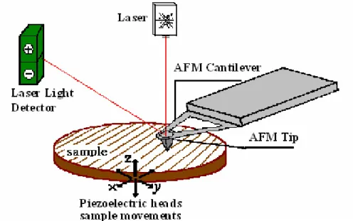
3.2 Atomic Force Microscope (AFM)
AFM consists of a scanning sharp tip at the end of a flexible cantilever across a sample surface while maintaining a small, constant force. The tips typically have an end radius of 2 nm to 20 nm, depending on tip type. The scanning motion is conducted by a piezoelectric tube scanner which scans the tip in a raster pattern with respect to the sample (or scans to the sample with respect to the tip). The tip-sample interaction is monitored by reflecting a laser off the back of the cantilever into a split photodiode detector. By detecting the difference in the photodetector output voltages, changes in the cantilever deflection or oscillation amplitude are determined. A schematic diagram of this mechanism is depicted in Fig. 3.1.
Fig. 3.1. Concept of AFM and the optical lever.
The two most commonly used modes of operation are contact mode AFM and TappingModeTM AFM, which are conducted in air or liquid environments. Contact mode AFM consists of scanning the probe across a sample surface while monitoring the change in cantilever deflection with the split photodiode detector. A feedback loop maintains a constant cantilever deflection by vertically moving the scanner to maintain a constant photodetector difference signal. The distance the scanner moves vertically at each x, y data point is stored by the computer to form the topographic image of the sample surface. This feedback loop maintains a constant force during imaging, which typically ranges between 0.1 to 100nN.
TappingMode AFM consists of oscillating the cantilever at its resonance frequency (typically ~300kHz ) and lightly “tapping” on the surface during scanning. The laser
deflection method is used to detect the root-mean-square (RMS) amplitude of cantilever oscillation. A feedback loop maintains a constant oscillation amplitude by moving the scanner vertically at every x, y data point. Recording this movement forms the topographical image. The advantage of TappingMode over contact mode is that it eliminates the lateral, shear forces present in contact mode, enabling TappingMode to image soft, fragile, and adhesive surfaces without damaging them, which can be a drawback of contact mode AFM.
3.3 Cell Gap Measurement System
For liquid crystal display, the thickness of cell gap usually affects the optical performance. Especially for SSFLC, the suppressing of helical structure needs a very small cell gap and, in addition, the gap between the two alignment layers would also influence the orientation of FLC. Thus, every time before the infection of FLC we need to measure the empty cell gap, and interferometric method [32] is what we use. The measurement instrument used is UV/Vis spectrometer LAMBDA 650 from Perkin Elmer, and the principle of this method is introduced as below.
The basic concept of the measurement method is based on the interference of light reflected by the two reflecting surfaces. The illustration is as Fig.3.2. R1, a coefficient of reflection, is defined as ratio of the light reflected by surface 1 to the incident light. R2 is the reflection coefficient of surface 2.
Fig.3.2. Two reflecting surfaces separated by a layer causing a light interference. The dotted
line indicates the first internal reflection [32].
If the total incident light is I =cosωt and we assume there is no any absorption of
light in surface 1and 2, then we can write the total reflected light R as
(
)
(
o)
k k k k kt t R R R t R R= + − − + ∞ = −∑
ω ω 1 cos cos 1 1 1 2 1 1 1 (3-1) Where ω 2π 2/λ 1 gap cn= and t 2dgapngap2/c
1
the wavelength, dgap is the thickness of the layer, ngap is the refractive index of the layer.
The cosine factor in Eq. (3-1) for k>1 are caused by internal reflections. Since R1<1 and R2<1, the magnitude of the cosine factors for k>1 is much smaller than for k=1. Therefore the internal reflection is chosen to be neglected, so
(
)
⎟⎟ ⎠ ⎞ ⎜⎜ ⎝ ⎛ − − + = λ π ω ω ngapdgap t R R t R R 1cos 1 1 2 2cos 4 (3-2)Thus the reflected spectrum is
( )
λ 2 R12[
(
1 R1)
2R2]
2 2R1(
1 R1)
2R2 cos(
4πngapdgap/λ)
R = + − + − × (3-3)
The periodic term in Eq.(3-3) causes an interference pattern. The periodicity of the reflected interference spectrum determined the optical thickness of the cell gap, ngapdgap.
If λ1 and λ2 are the two wavelengths showing extrema in Eq.(3-3), then
(
4 /)
1cos πngapdgap λ =± for λ =λ1and λ =λ2. Therefore 2 / 2ngapdgap =k1λ1 (3-4) 2 / 2ngapdgap =k2λ2 (3-5)
Where k1 and k2 are natural numbers. Supposeλ1 >λ2, then x
k
k2 = 1+ (3-6)
Where x is a natural number.
Based on Eqs.(3-4), (3-5), and (3-6), we can write
(
1 2)
2 1 4λ λ λ λ − = x d ngap gap (3-7)The value of x-1 indicates the number of extrema in R
( )
λ 2 between the wavelengths λ 1and λ . It is better to choose the distance x between the two extrema as large as possible for 2 improving the accuracy of the calculation ofngapdgap. The sample data was shown in Fig.3.3
Fig.3.3. The reflection as a function of wavelength using a air gap of 5.0μm.
3.4 Laser Optics Systems
Our laser optics system is as in Fig.3.4. This optical system is responsible for the measurement of electro-optical properties, such as V-T characteristics and response time. First of all, we have to reduce the intensity of laser source within the acceptable range of the photo detector by using a 10% ND filter. Next, the moderate unpolarized light becomes a polarized light after passing through the polarizer and then enters the LC cell. The LC cell, acted as a phase modulator, changes the phase of the incident polarized light by retardation Δn⋅d (Δn
is the birefringence of LC, and d is the thickness of LC). Then the modulated light passes through the analyzer and the light output is received by the photo detector. The driving waveform of FLC is written by ourselves and sent by a waveform generator WFG500 (from FLC Electronics AB). The optical output received by the photo detector can be observed with the oscilloscope (from Tektronix) and quantified data can be read by a multimeter (from Keithley).
We use a bipolar square wave with various frequencies, applying on the cell, to measure the response time of the test cell. The V-T curve is measured by using a 0.1 Hz bipolar triangular wave.
Sending data Polarizer Analyzer Sample Photodetector PC Waveform generator Oscilloscope Sending signals Ch1 Ch2 Multimeter He-Ne Laser Sending waveform Sending data ND filter Sending data Sending data Polarizer Analyzer Sample Photodetector PC Waveform generator Oscilloscope Sending signals Sending signals Ch1 Ch1 Ch2Ch2 Multimeter He-Ne Laser He-Ne Laser Sending waveform Sending waveform Sending data Sending data ND filter
Fig.3.4. A schematic diagram of the laser optics system.
3.5 ConoScope
Fig.3.5.The schematic diagram of ConoScope.
The ConoScope (autronic-MELCHERS GmbH) can be used for visual performance evaluation, such as luminance, contrast ratio, color shift, gray scale and many characteristics.
The basic operating principle of the ConoScope is described as follows. A typical scanning device (so-called “gonioscopic system”) would scan the half cone above the display to detect the variations of luminance and color for each specific direction. Plotting each azimuthal angle on a circle with the radius from the center additionally indicates the polar angle results in the so-called polar coordinate system. Using such a polar plot to mark for each direction luminance and /or color will result in (in the case of color) a colored figure.
An arrangement of several lenses (here represented by single lens) modifies the light propagation directions in a way, that all beams emerging from the sample in the same direction will meet in one spot in the focal plane (or within the “conoscopic figure”) corresponds to one specific direction of the viewing cone. The conoscopic figure directly shows color and luminance as they would have been plotted in a polar coordinate system as described under Fig.3.6. In our measurement, we used the collimated illumination as the backlight for the transmissive mode to analyze the luminance, contrast ratio, and light distribution of the FLCD.
Chapter 4
Experiments and Results
4.1 Introduction
For the fast sub-millisecond switching FLCD, the major problem degrading the performance is the alignment defects that cause light leakage in the dark state and result in low contrast. In this thesis, three alignment issues that directly relate to the orientation of SSFLC were discussed. One of the issues is the sign of the surface polarity which could probably results in Ps attraction [33] or repulsion; another one is surface roughness which affects the effective surface pretilt [25][34]; the other one is the surface rubbing conditions, that is, rubbing direction and rubbing strength.
As mentioned in the section 2.2.3, the formation of horizontal chevron defect results from the random orientation of Ps which means that layer structures in opposite directions show up randomly. In the following sections, a new hybrid cell structure was applied to effectively orient the Ps and to obtain a uniform uni-direction layer. On the other hand, to achieve a zigzag free orientation the C2 uniform structure is preferred because the alignment is relatively simple and it is much easier to avoid twist state in C2 than in C1 [8]. In C2 state small surface roughness is an essential criteria, thus two methods were tried to improve the surface roughness.
4.1.1
Cell Fabrication Process
The flow chart shown as below is the fabrication process of our liquid crystal cell:
A. Each piece of glass is rinsed with detergent and rubbed by hands carefully. Then, wash the glass with DI water until the water flowing along the surface smoothly. After that, put the glass loaded with a holder into hot DI water and shake it with ultra sonic for 30 minutes.
B. Blow the surface of glass with nitrogen gas to rip off the water, and then bake for 1 hour at 110℃. Next, use UV-ozone to treat surface for 10 minutes (that is for better adhesion of alignment layer).
C. Put the clean ITO glass onto the spin coater. Drop the solution of alignment material (make sure the solution to cover the whole glass), then spin. The procedure of spin-coating is as follows:
2.5wt%PVA Polyimide
Speed Time Speed Time
1st spin 500rpm 10s 1st spin 500rpm 10s
2nd spin 1500rpm 20s 2nd spin 5000rpm 20s
After spin-coating, we need to bake the samples for full adhesion for a short time, which is 30 minutes at 110℃ for PVA and 30 minutes at 200℃ for polyimide. PVA (Mw Cleaning of
ITO glass
Coating of
alignment film Baking Rubbing
Spacer placing with UV glue Press uniformly UV curing for adhesion Cell gap measurement LC injection Annealing Measuring of E-O properties
13,000-23,000, 98% hydroldyzed) is from Sigma-Aldrich, and polyimide (PIA-X201-G01) is from Chisso. The film thickness, which is measured by AFM (from Digital Instruments), of 2.5wt% PVA is 1000Å, and the thickness of 50wt% polyimide is about 350Å.
D. Rub the samples with rubbing machine. The rubbing strength is different depending on the LC material, alignment film, and pretilt angle. The rubbing condition used is as below:
E. Drop a small amount of UV glue (NOA-65, from Norland) mixing with 1.6um spacer at the four corner of the bottom plate. Cover the top plate and press. Next, place the cell under a UV lamp for 5 minutes to fully cure the glue, and then an empty cell is done. F. Measure the cell gap of an empty cell by spectrometer UV-Vis 650 (from Perkin Elmer)
using interferometric method. The details will be explained in section 3.2.4.
G. Heat up the cell and LC material to the temperature above the clearing point. Inject the LC material from the edge of the cell until the LC is full of the gap.
H. Anneal the cell carefully with programmable hot plate from high temperature to room temperature. The annealing process depends on the phase sequence of the LC material. I. Solder the wire at the ITO contact, and then the test cell is available for a mount of
electro-optical measurements.
4.1.2
Measurement of Sign of Surface Polarity
Since we proposed the hybrid cell structure to align Ps in section 2.4, the sign of surface polarity played an important role. In order to check the sign of the surface polarity of
PVA Polyimide
Pile impression 0.23mm Pile impression 0.2mm
Rotation speed 300rpm Rotation speed 300rpm
alignment layer, two crossed-rubbing cells were made. One of the cells has PVA coating on both substrates, as in Fig.4.1 (a), and the other one has PI coating on both substrates, as in Fig..4.1 (b). After filling the FLC material with positive Ps into the cross-rubbing cell, a twisted structure was formed. According to the sign of surface polarity, the Ps of molecules at the top and bottom surface directed inward or outward the cell. In addition, based on the switching nature of FLC, a specific layer direction should be observed in the cross-rubbing cell and layer normal of FLC in PVA cell would be perpendicular to one in PI cell. The FLC material used is R3206, with Ps~18 nC/cm2. After injecting the FLC and cooling down the cells to room temperature, we found that the layer was formed and the layer normal direction of PVA cell was perpendicular to PI cell, as shown in Fig.4.2. The results matched the assumption in Fig.4.1. According to the results, sign of the surface polarity was confirmed.
Fig.4.1. The illustration of twisted structure in crossed-rubbing (a) PVA cell and (b) PI cell.
(a)
(b)
Fig.4.2. Pictures of the cross-rubbing cells taken by POM. Pictures at the right are the
4.1.3
Observation of CDR Type FLC Cells
Since the relationship between Ps and the sign of the surface polarity was revealed, the uni-direction layer model could be applied first on the test cell with CDR type FLC. Two FLC materials would be used─R2301 (from Clariant) and R3206 (from AZ Electronic Materials). R2301 has phase sequence, I 86.8-84.8 N* 64.7 SmC* and R3206 has phase sequence, I 107-105.4 N* 78.4 SmC* -12(-6) Cr. The filling process was as below: First, the FLC material was injected to the hybrid cell by capillary force in isotropic state. Then the test cell was annealed in N* phase for 5 minutes and annealed in SmC* phase for 30 minutes. Finally, the test cell was cooled down to the room temperature.
OFF STATE
ON STATE
Fig.4.3. (a)(c) is the OFF and ON state of R2301 in hybrid cell, and (b)(d) are the OFF and
After the filling of the two FLC materials, the test cells were observed under polarizing optical microscope (POM) and it was found that a uni-direction layer structure was formed both with R2301 and R3206, as shown in Fig. 4.3. Fig. 4.3 (a)(b) showed the OFF states between cross-polarizer and Fig. 4.3 (c)(d) showed the ON states with application of 100 Hz square wave. As compared with Fig.4.3 (a), the microdomain structure in Fig.4.3 (b) was more obvious, although uni-direction layer was obtained in both cells.
Contrast and viewing angle
To see how much the contrast can be raised by the hybrid cell structure, we have measured the symmetrical cell 71 with R3206, hybrid cell 97 with R3206, symmetrical cell 59 with R2301 and hybrid cell 98 with R2301, as shown in Fig.4.4-Fig.4.7. The symmetrical cell 59 and 71 with horizontal chevron defect showed poor contrast (CR~29 for cell59;CR~18 for cell71). On the other hand, an improved contrast (CR~86) was shown in cell 97 with R3206, and the highest contrast (CR~144) was performed in cell 98 with R2301. As for viewing angle, because of the quasi in-plane switching and small surface pretilt the viewing angle could reach over ±70°.
Besides, the switching mechanism could be observed in conoscopic pictures. In Fig.4.5 and Fig.4.7, we saw the asymmetric light distribution of the ON state which was resulted from a tilted uni-layer structure, as shown in Fig.2.12 (a)(b), leading to an asymmetric switching cone. On the contrary, as shown in Fig.4.4 and Fig.4.6, the light distribution of the ON state showed symmetry which was considered as the averaged switching of two different layers in horizontal chevron. Thus, according to the conoscopic pictures, the uni-layer structure was also confirmed.
Fig.4.4. CR v.s. viewing direction of symmetrical cell 71 with R3206.
Fig.4.5. CR v.s. viewing direction of hybrid cell 97 with R3206.
Fig.4.7. CR v.s. viewing direction of hybrid cell 98 with R2301.
4.1.4
Observation of FGLC Series Cells
The self-made FGLC mixtures[37]show wide smectic C temperature range and good alignment ability. The 2%FGLC-1 mixture shows V-shaped switching and has SmA phase in the phase sequence. We filled 2%FGLC-1 mixture into hybrid (PVA/PI) cell, and the orientation of uni-direction layer was observed under POM as shown in Fig.4.8. Picture at the right is the ON state which is driven by a 100Hz 17V square wave, and the picture at the left is the OFF state under crossed polarizer. Although hybrid cell structure seemed successful on 2%FGLC-1 mixture, we found that after driving for a long time some stripe defect appeared, as shown in Fig.4.9, and the higher the driving voltage was applied the faster the stripe defect showed up. The stripe defect usually grows from the boundary between the two different domains, but sometimes grows from the center of the well-aligned domain. The growing direction of defects is parallel to the rubbing direction. The reason of defect formation will be discussed in section 4.4.
Fig.4.8. The alignment of 2%FGLC-1 in 1.78um hybrid cell. (a) Dark state. (b) Bright state.
Fig.4.9. (a) Before driving. (b) After driving, the stripe defect grows along the rubbing
direction during driving.
4.1.5
EO Properties of FGLC Series Cells
To see if the hybrid cell structure affect the electro-optical properties of SSFLC or not, the response time of 2%FGLC-1 in 2um hybrid cell has been measured using various frequencies, as shown in Fig.4.11. Also the response time of 2%FGLC-1 in symmetric cell was listed in Table.4.2. During the measurement of response time, two conditions, as shown in Fig.4.10, were tried: 1) The positive field direction of applied square wave was “parallel” to the Ps direction. 2) The positive field direction of applied square wave was “opposite” to the Ps direction.
Fig.4.10. Response time measurement conditions: (a) The positive field direction of applied
square wave is parallel to Ps (b) The positive field direction of applied square wave is opposite to Ps
The response time of 2%FGLC-1 was found faster in hybrid cell than in symmetric premade cell. And it was found that when the positive field of applied square wave is opposite to the direction of Ps, the fall time would be faster. We supposed that after removing the voltage the director returned to the initial state more quickly because the asymmetric polarity in hybrid cell provided a restoring force. In addition, if the positive field of applied square wave is opposite to the direction of Ps, the rise time would be slower, comparing to cell with positive field of applied square wave parallel to the direction of Ps. It was inferred that because of the asymmetric polarity of the cell, a dragging force slowed down the switching when field opposite to the direction of Ps was applied.
Table.4.1. Response time of 2%FGLC-1 in 2μm premade cell driven by 1kHz 30V square
wave. Both of the two alignment films in premade cell are the same. Response time
Material
Rise time(τ10-90) Fall time(τ90-10)
2%FGLC-1 680us 1.1ms
0 200 400 600 800 1000 100 160 1000 Driving frequency (Hz) R is e tim e (m ic ro n s) Ps opposite to +E Ps parallel to +E 0 200 400 600 800 1000 1200 100 160 1000 Driving frequency (Hz) F all tim e ( m icr on s ) Ps opposite to +E Ps parallel to +E
Fig.4.11. Response times for the (a) rising process and the (b) falling process of 2%FGLC-1
in 2μm hybrid cell driven by a 30V bipolar square wave with various frequency. Blue dot is the data measured when the direction of positive electric field is opposite to the direction of Ps. Pink square is the data measured when the direction of positive electric field is parallel to
the direction of Ps.
4.2 Improvement of Surface Roughness
To fulfill the criterion of C2 uniform state, it is known that the pretilt angle of the alignment film must be small [38]. However, even if the pretilt angle of alignment film is small, a uniform C2 structure would still not be obtained with a rough surface because the
(a)
local surface variation changes the surface pretilt [25][34]. H. Furue et al. obtained a zigzag free C2 structure by using a very smooth alignment film [25]. Based on this concept, we wondered to achieve a smooth and uniform alignment surface by coating an additional layer which could flatten the surface and has alignment ability.
4.2.1 High T
gLC Coating
The first material we used was oligoflourene [39], F(Pr)5F(MB)2, which has a high glass transition temperature, Tg, at 149 °C and a nematic-to-isotropic transition temperature,
Tc, at 366 °C. The coating of high Tg LC had two purposes: 1) since oligoflourene could
achieve monodomain [39], the well aligned surface would probably provide a smooth surface. 2) Liquid crystal with high Tg could preserve its alignment at temperature higher than the
nematic-to-isotropic temperature of the FLC materials. Thus, the alignment of oligoflourene would maintain during FLC filling process.
Thin film of oligofluorene was prepared by spincoating from 0.25 wt% solution in chloroform at a spin rate of 1500 rpm. The oligoflourene film coated on rubbed polyimide had thickness about 20nm to 30nm. Afterward, annealing at a temperature slightly above Tg was
performed to well align the molecules. In Fig.4.12 the surface roughness was reduced due to additional layer coating. The UV-ozone treatment is needed to rip off the residual organics on the surface and to enhance the adhesion of alignment layer when coating. After coating PI, the surface mean roughness was reduced from 5.917nm to 0.692nm. Moreover, the coating of oligoflourene reduced the mean roughness to 0.345nm. The surface morphology was measured by Atomic Force Microscope (AFM).
Fig.4.12. The surface morphology of layer (a) with no treatment, (b) treated by UV-ozone, (c)
coating with polyimide after UV-ozone treatment, and (d) coating with oligoflourene on rubbed polyimide.
We used the oligoflourene-coated substrate to replace one side or both sides of the cell and filled the FLC materials. The cell was observed by POM and it seemed the alignment was improved somewhere, as shown in Fig.4.13 (a). However, it was found that a part of the FLC materials would dissolve oligoflourene and mixed together, which destroyed the alignment as shown in Fig.4.13 (b). The reason of the mixing may be the π-π interaction between benzene rings of the FLC material and oligoflourene.