Direct current circuit simulation model for a field emission triode
Chih-Wen Lu and Chung Len Lee
Citation: Journal of Vacuum Science & Technology B 16, 2876 (1998); doi: 10.1116/1.590241
View online: http://dx.doi.org/10.1116/1.590241
View Table of Contents: http://scitation.aip.org/content/avs/journal/jvstb/16/5?ver=pdfcov Published by the AVS: Science & Technology of Materials, Interfaces, and Processing
Articles you may be interested in
Modeling of emitted current distribution and electron trajectories in the thin-film field-emission triode J. Vac. Sci. Technol. B 22, 1250 (2004); 10.1116/1.1736636
Field-emission triodes with integrated anodes
J. Vac. Sci. Technol. B 18, 914 (2000); 10.1116/1.591297 Characteristics and circuit model of a field emission triode J. Vac. Sci. Technol. B 16, 916 (1998); 10.1116/1.589930 Numerical modeling of the disk-edge field emitter triode J. Vac. Sci. Technol. B 15, 394 (1997); 10.1116/1.589324
Simulation of field emission and electrodynamic characteristics for triode near-cathode modulators with edge field emitter arrays
Chih-Wen Lu and Chung Len Leea)
Department of Electronics Engineering, National Chiao Tung University, Hsinchu, Taiwan, Republic of China
~Received 12 January 1998; accepted 26 June 1998!
A simple empirical circuit model, which can be incorporated into circuit simulation programs such asSPICE, for a field emission triode is developed. The model is based on the Fowler-Nordheim~FN!
J-E relationship but takes into account the space charge effect and the exponential-like charge
distribution on the surface of the tip of the device. A procedure is also developed to extract the parameters of the model. © 1998 American Vacuum Society.@S0734-211X~98!02105-2#
I. INTRODUCTION
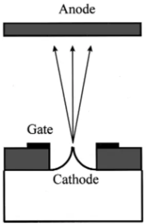
A field emission triode~FET! is a solid-state device which features a miniature vacuum tube triode formed by the appli-cation of modern integrated circuit ~IC! processing technol-ogy. A typical FET consists of a cathode, a control gate and an anode similar to that of a conventional vacuum tube tri-ode, as shown in Fig. 1. When a moderate voltage is applied between the gate and the cathode, a very large electric field is formed on the tip of the cathode due to the sharp geometry of the tip and the short gate-to-cathode distance. An electron will be emitted from the surface of the cathode following the Fowler-Nordheim tunneling mechanism to the anode which is biased at a proper high voltage.1–3However, since the gate is always biased more positively than the cathode, large gate currents can flow at zero and moderate positive anode volt-age. The cathode current characteristics, the gate current characteristics, and the output characteristics are shown in Figs. 2~a!–2~c!, respectively.4 As the anode voltage de-creases, the anode current decreases and the gate current in-creases. The cathode current is always equal to the anode current plus the gate current.
Applications of FET circuits have triggered a demand for circuit simulation, which requires an efficient and accurate FET model. Some work was done on FET modeling.5–7For example, based on the ideal field emitter floating sphere model, Nicolaescu and Avramescu5developed a field emis-sion diode model. Jones et al.6developed a circuit model for a FET array operating at low voltage and characterized the model parameters by using theoretical and experimental techniques. Qin et al.7 also developed a model for the FET amplifier. However, all these models are either fairly com-plicated or physical structure dependent and none of the models includes the space charge effect which makes the J-E relationship of the device deviate from the Fowler-Nordheim
~FN! J-E relationship in the high gate voltage region.8,9 In this work, we propose a FET model which is based on the FN J-E relationship but takes into account the space charge effect and the exponential-like charge distribution on the surface of the tip of the device.9 The model is simple, accurate and easy to incorporate into a circuit simulation program such asSPICE.
II. DEVICE MODEL
The proposed device equivalent circuit is shown in Fig. 3. The anode and gate currents are both functions of anode voltage Va and gate voltage Vg. The anode current can be
obtained by subtracting the gate current from the cathode current.
The cathode current Ic, mainly based on the
Fowler-Nordheim relationship, is expressed as
Ic~Vg!5AcVg 2 exp
F
2Bc Vg 2C expS
D VgDG
, ~1!where Acis a parameter related to the field enhanced
param-eter a and the effective emission area b by;b/a2, Bcis Eca,
where Ecis the critical electrical field,
10–14
and C and D are two parameters related to the space charge effect. When the device is operated at low gate bias, C and D are zero and Eq.
~1! can be simplified to Ic~Vg!5AcVg2 exp
F
2BcVg
G
, ~2!
which is the typical FN equation.2,3,10,15 In the above equa-tions, the cathode voltage is assumed to be the reference grounded voltage.
Figure 4 shows the FN plot of the cathode current of the experimental device of Figs. 2~a!–2~c!.4In the plot, it can be seen that the plot is a straight line at the low gate voltage region and bends at the high gate voltage region due to the
space charge effect. From this plot, parameters Ac, Bc, C and D can be determined, which will be explained in Sec. III. The cathode current is shared by the anode and the gate. It is known that the gate current equals the cathode current when the anode voltage is zero. That is,
Ig~Va50!5Ic. ~3!
The above equation can be considered to be the boundary condition for deriving the gate current expression.
At the above boundary condition, the gate current expres-sion should be the same as that of the cathode current, i.e.,
FIG. 2. ~a! Characteristics of the cathode current of a FET measured with gate voltages varying from 60 to 78 V.~b! Characteristics of the gate current of the same device for which, as the anode voltage increases, the gate current decreases.~c! Output characteristics of the same device for which, as the anode voltage increases, the anode current increases.
FIG. 3. Proposed device equivalent circuit. The cathode and gate currents are both functions of anode voltage Vaand gate voltage Vg. The anode current can be obtained by subtracting the gate current from the cathode current.
FIG. 4. FN plot of the cathode current of an experimental device operating at
Va5200 V. The plot is a straight line at the low gate voltage region and bends at the high gate voltage region due to the space charge effect.
2877 C.-W. Lu and C. L. Lee: dc circuit simulation model 2877
Ig~Va50,Vg!5Ag~Va50!Vg 2 exp
F
2Bc Vg2C 3expS
2 D VgDG
, ~4!where Ag(Va50)5Ac and it is also related to the field
en-hanced parameter and the effective emission area. The field enhanced parameter should be the same as that in the cathode current expression. The effective emission area is dependent on the anode and gate voltages. A larger gate voltage and a smaller anode voltage give a larger gate current. So, Ag is a function of Vg and Va. The current density distribution of the surface of the tip is an exponential-like decay.9 We ex-press Ag in the following form:
Ag5Acexp
S
E1Va1E2Va22F1Va1F2Va2
Vg
D
, ~5!
where E1, E2, F1and F2are parameters to be used to fit the effective emission area of the gate current. When the anode voltage is not zero, the gate current can be expressed as
Ig~Va,Vg!5AcVg 2 exp
F
E1Va1E2Va 2Bc1F1Va1F2Va 2 Vg 2C expS
2VD gD
G
. ~6!The anode current can be obtained by subtracting the gate current Ig from the cathode current Ic, i.e.,
Ia5Ic2Ig. ~7!
III. PARAMETER EXTRACTION
As mentioned previously, the parameters can be extracted in values from the measured cathode current and gate current in the FN plots of an experimental device. To describe the procedure more clearly, device data which were published in the literature are used as examples for the demonstration.
The first device example used is that published in Betsui’s paper.4 The device was a silicon field emitter array of 6400
~80380! tips. The radius of the bullet-shaped tip was less
than 20 nm. The spacing between tips was 4 mm, so the tip density was 6.253106 cm22. The diameter of the gate aper-ture was 2 mm, which was larger than that of its silicon dioxide mask. The distance between the anode plate and gate was 1 mm. In Betsui’s measuring apparatus, the gate was grounded and negative voltage was applied to the cathode to extract electrons. In this work, the cathode voltage is as-sumed to be the reference grounded voltage. The cathode, the gate, and the output I-V characteristics are those shown in Figs. 2~a!–2~c!, respectively.
In Eqs.~1! and ~6!, Ac, Bc, C, D, E1, E2, F1and F2are unknown parameters. From the FN plot of Fig. 4, the values of Ac and Bc can be obtained from the slope and the
inter-cept of the coordinate axis in the nonspace charge region.16 The values of Ac and Bc are 1.2131022 A/V2 and 7.81
3102 V, respectively.
The values of parameters C and D can be extracted by rearranging Eq. ~1! as
FIG. 5. Plot of the difference between ln Ac2 (Bc/Vg) and ln(Ic/Vg
2) with
respect to 1000/Vgfrom which the values of C and D can be extracted. FIG. 6. FN plot of the gate current of the experimental device for several
Va’s from which the values of the anode-voltage-dependent factors, ln Ac
1E1Va1E2Va
2
and Bc1F1Va1F2Va
2
, are calculated from the slope and the intercept of the coordinate axis for each anode voltage.
TABLEI. Extracted values for the device model parameters of the experi-mental device of Ref. 4.
Parameter Value Ac 1.2131022A/V2 Bc 7.81310 2 V C 3.5631012 D 443103V E1 2.9231021V21 E2 2.8731024V22 F1 2.27310 1 F2 3.9331022V21
ln Ac2 Bc Vg 2ln Ic Vg25C exp
S
2 D VgD
. ~8!Since Ic is measured data and the Ac and Bc values are
already known, the difference between ln Ac2 (Bc/Vg) and
ln(Ic/Vg
2) can be plotted as shown in Fig. 5, which is an exponential decay curve against 1000/Vg. The values of C
and D can be easily extracted from this plot.
The values of the gate current parameters, E1, E2, F1and
F2, can be obtained by a similar procedure. Taking the natu-ral logarithm and rearranging the gate current expression of Eq. ~6!, we obtain ln Ig Vg21C exp
S
2 D VgD
5ln Ac1E1 Va1E2Va 2 2Bc1F1Va1F2Va 2 Vg , ~9!where Igis measured data. The values of E1, E2, F1, and F2 can be obtained by plotting ln(Ig/Vg2)1C exp2 (D/Vg) against 1/Vgfor each anode voltage Vain Eq.~9!. Figure 6 is the FN plot for an experimental device for several Va’s. The
values of the anode-voltage-dependent factors, ln Ac1E1Va
1E2Va
2 and B
c1F1Va1F2Va
2, can be calculated from the slope and the intercept of the coordinate axis for each anode voltage. Then, the values of E1, E2, F1, and F2 can be extracted. The values derived for all the parameters are sum-marized in Table I.
The experimental device above was used to extract the values of the parameters in Eqs. ~1!, ~6! and ~7!. The values obtained can be used to reconstruct the characteristics of the device. Figure 7 shows the reconstructed output characteris-tics~the solid curves! of the device along with the originally measured output characteristics~the dotted curves!. Two sets of characteristics match very well.
To verify the validity of this model for a field emission cathode operated in the space charge region, a second ex-ample is also given. Figure 8 shows the I-V characteristics of a Spindt-type FET with a single emitter,9 where the open circle curve are the data points obtained from Ref. 9 and the
FIG. 7. Reconstructed output characteristics ~solid curves! simulated from the extracted values of the circuit parameters and the original measured output characteristics~dotted curves!. Two sets of characteristics match very well.
FIG. 8. I-V characteristics of a Spindt-type FET with a single emitter~Ref. 9!. The open circle curve is the data points obtained from Ref. 9 and the solid line is the reconstructed curve from Eq.~1!.
FIG. 9. I-V characteristics of a FET triode with 100 emitter tips. The square curves are the data points obtained from Ref. 17 and the solid lines are reconstructed curves from the model.
TABLEII. Extracted values for the device model parameters of the
experi-mental device of Ref. 9.
Parameter Value Ac 1.0131022A/V2 Bc 5.20310 2V C 1.113101 D 5.883102V
2879 C.-W. Lu and C. L. Lee: dc circuit simulation model 2879
solid line is the reconstructed curve from Eq.~1!. At the high field region where the space charge effect becomes evident, the I-V deviates from the Fowler-Nordheim straight line characteristics. The two curves show a good match. The val-ues derived for the parameters are summarized in Table II.
A third example of a FET of a different emitter geometry is also used to verify the model. Figure 9 shows the I-V characteristics of a FET triode with 100 emitter tips and a separate anode in the form of a tube located 5 mm from the gate electrode,17where the square curves are the data points obtained from Ref. 17 and the solid lines are reconstructed curves from the model. This device operates only in the non-space charge region. So the values of parameters C and D are zero. Two sets of curves also agree with each other well. The values derived for the parameters are summarized in Table III. This example also demonstrates that the model is appli-cable to a FET with emitters of tube geometry.
IV. CONCLUSION
In this work, a simple empirical model for a FET device has been developed. The model can be used in circuit simu-lation programs such as SPICE. For the model, the cathode current is based on the FN relationship but takes into account the space charge effect, and the gate current, which is also based on the FN relationship through the boundary
condi-tion, Ig(Va50)5Ic, considers the exponential-like decay of the charge distribution on the surface of the tip of the device. A procedure to extract the values for the model parameters has also been demonstrated. To obtain the model parameters, six sets of measurements for different gate voltages, three sets for the nonspace charge region and three sets for the space charge region are needed. The model has been applied to experimental FET devices of different geometries, namely, an emitter array, a single emitter and a tube type of anode, to show its applicability. From the successful appli-cation to the three device examples of different geometries, it can be said that this model can be applied to describe the Spindt-type FETs.
1R. H. Fowler and L. Nordheim, Proc. R. Soc. London 119, 173~1928!. 2C. A. Spindt, I. Brodie, L. Humphrey, and E. R. Westerberg, J. Appl.
Phys. 47, 5248~1976!.
3
W. J. Orvis, C. F. McConaghy, D. R. Ciarlo, J. H. Yee, and E. W. Hee, IEEE Trans. Electron Devices 36, 2651~1989!.
4K. Betsui, Technical Digest of IVMC’91, 1991, pp. 26–29.
5D. Nicolaescu and V. Avramescu, J. Vac. Sci. Technol. B 12, 749~1994!. 6
R. D. Jones, R. K. Feeney, J. K. Cochran, and D. N. Hill, Technical Digest of IVMC’95, 1995, pp. 72–76.
7M. Qin, Q. A. Huang, and T. L. Wei, Technical Digest of IVMC’96,
1996, pp. 86–90.
8R. True, Tech. Dig. Int. Electron Devices Meet., 1992, p. 379. 9
G. N. A. Van Veen, J. Vac. Sci. Technol. B 12, 655~1994!.
10E. A. Adler, Z. Bardai, R. Forman, D. M. Goebel, R. T. Longo, and M.
Sokolich, IEEE Trans. Electron Devices 38, 2304~1991!.
11H. H. Busta, D. W. Jenkins, B. J. Zimmerman, and J. E. Pogemiller, Tech.
Dig. Int. Electron Devices Meet., 1991, p. 213.
12
H. H. Busta, D. W. Jenkins, B. J. Zimmerman, and J. E. Pogemiller, IEEE Trans. Electron Devices 39, 2616~1992!.
13H. H. Busta, J. E. Pogemiller, and B. J. Zimmerman, IEEE Trans.
Elec-tron Devices 40, 1530~1993!.
14
D. Nicolaescu, Technical Digest of IVMC’94, 1994, pp. 139–142.
15D. A. Kirkpatrick, A. Mankofsky, and K. T. Tsang, Appl. Phys. Lett. 60,
2065~1992!.
16J. M. Houston, Phys. Rev. 88, 349~1952!. 17
C. E. Holland, A. Rosengreen, and C. A. Spindt, IEEE Trans. Electron Devices 38, 2368~1991!.
TABLEIII. Extracted values for the device model parameters of the
experi-mental device of Ref. 17.
Parameter Value Ac 3.4431025A/V2 Bc 1.79310 3V E1 5.3131021V21 E2 25.9731023V22 F1 1.073102 F2 21.09 V21