國
立
交
通
大
學
資訊科學與工程研究所
碩
士
論
文
32 位元雙軌之靈活的運算邏輯單元實作
A Flexible Dual-rail 32-bit ALU Design
研 究 生:方秋鈞
指導教授:陳昌居 教授
中 華 民 國 九 十 七 年 六 月
A Flexible Dual-rail 32-bit ALU Design
研 究 生:方秋鈞 Student:Chiou-Ching Fang
指導教授:陳昌居 Advisor:Chang-Jiu Chen
國 立 交 通 大 學
資 訊 科 學 與 工 程 研 究 所
碩 士 論 文
A Thesis
Submitted to Institute of Computer Science and Engineering College of Computer Science
National Chiao Tung University in partial Fulfillment of the Requirements
for the Degree of Master
In
Computer Science June 2008
Hsinchu, Taiwan, Republic of China
32 位元雙軌之靈活的運算邏輯單元實作
研究生: 方秋鈞
指導教授:陳昌居教授
國立交通大學
資訊科學與工程學系碩士班
摘要
通常來說ALU對於處理器的效能是個瓶頸,所以能夠有效提升ALU的效能對於處理 器整體效能的提升有一定的幫助。然而在同步電路設計上,整體的速度往往是由最慢的 元件所決定。但是對於非同步電路設計而言,再前一筆資料處理完之後便能立刻去處理 下一筆需要處理的資料。所以整體效能是隨著資料的複雜性而有所不同而不會綁在最長 的延遲時間上,因此效能上較趨向於平均延遲時間而非最長延遲時間。 於是在本篇論文中便引入非同步電路設計的概念來幫助我們提升ALU的效能。而其 構想是來自於DSP處理器中常用到的MAC指令。MAC指令是一個先做乘法再將所得的結 果作加法的兩階段指令。我們將此想法加以應用並設計一個包含兩個階段的ALU。此設 計的優點在於其指令格式和延遲時間上更具有彈性。A Flexible Dual-rail 32-bit ALU Design
Student : Chiou-Ching Fang
Advisor : Dr. Chang-Jiu Chen
Department of Computer Science and Information Engineering
National Chiao-Tung University
Abstract
Because ALU usually is the bottleneck of the processor performance, improving the processing time of ALU is also the chance to improve overall performance. In synchronous circuit design, the performance is determined by the slowest component. However, in an asynchronous circuit design, the next computation step can be started immediately after previous step has been completed.
Thus in this thesis we introduce the concepts of asynchronous circuit design to improve performance of ALU. The original idea of our design is derived from MAC related instruction supported by almost all DSP processors. Then we extend this idea to design our ALU composed of stages. The advantage of this kind of design is its flexibility on instruction types and delays.
Acknowledgment
本論文能夠順利完成,首先要感謝陳昌居老師這兩年來的指導,以及口試委員的寶 貴建議。再來要感謝緯民、元騰以及宏岳學長熱心的幫忙與建議,還有實驗室的同學及 學弟們,陪我度過這兩年愉快的研究所時光。最後要感謝家人的支持,讓我能安心的完 成學業。Contents
摘要 ...I ABSTRACT ... II ACKNOWLEDGMENT ... III CONTENTS ... IV LIST OF FIGURES ... VILIST OF TABLES ... VIII
CHAPTER 1. INTRODUCTION ... 1
1.1OVERVIEW ... 1
1.2MOTIVATIONS ... 2
1.3THE ORGANIZATION OF THIS THESIS ... 2
CHAPTER 2. BACKGROUND ... 3
2.1ASYNCHRONOUS CIRCUITS ... 3
2.1.1 Handshake Protocols ... 3
2.1.2 Classification of Asynchronous Circuits ... 7
2.2ASYNCHRONOUS PIPELINE ... 8
2.2.1 C-element ... 8
2.2.2 4-phase dual-rail Pipeline ... 9
CHAPTER 3. ANALYSIS AND IMPLEMENTATION ... 12
3.1OVERVIEW ... 12
3.2RESULT OF ANALYSIS ... 13
3.3INTERNAL STRUCTURE OF PROPOSED ALU ... 19
3.4.1 Completion Detection Circuit ... 23
3.4.2 Logical operation ... 24
3.4.3 Arithmetic operation ... 25
3.4.4 Barrel Shifter... 32
CHAPTER 4. SIMULATION RESULTS ... 38
CHAPTER 5. CONCLUSION... 41 REFERENCE ... 42
List of Figures
Figure 2-1: Categories of asynchronous handshake protocol ... 3
Figure 2-2: Bundled Data channel (a); 4-phase bundled-data protocol (b); 2-phase bundled-data protocol (c) ... 4
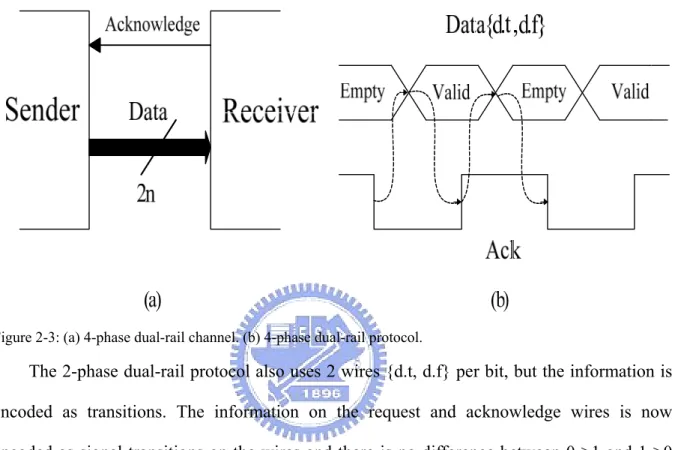
Figure 2-3: (a) 4-phase dual-rail channel. (b) 4-phase dual-rail protocol. ... 6
Figure 2-4: Illustration of the handshaking on a 2-phase dual-rail channel ... 7
Figure 2-6: C-element: (a) symbol; (b) possible implementation; (c) truth-table ... 9
Figure 2-7: A simple 3-stage 1-bit wide 4-phase dual-rail pipeline ... 10
Figure 2-8: (a) A 3-bit latch with completion detection. (b) Alternative completion detector ... 11
Figure 3-1: Compilation stages of GNU C/C++ Compiler ... 12
Figure 3-2: The percentages of each instruction categories ... 14
Figure 3-3: The execution sequence of MLA instruction ... 15
Figure 3-4: The idea which extends from MLA instruction ... 16
Figure 3-5: The process we transfer our idea to concrete design ... 18
Figure 3-6: Block diagram of internal structure of ALU ... 19
Figure 3-7: 1-bit-select Demux-Merge pair and its implementation ... 20
Figure 3-8: 1-bit-select Demux-Demux pair and its implementation ... 21
Figure 3-9: Self-timed component with completion detection circuit ... 24
Figure 3-10: The 2-input dual-rail AND gate ... 25
Figure 3-11: The work flow of conventional asynchronous multiplier ... 26
Figure 3-12: An 8*8 bits right-to-left array multiplier ... 27
Figure 3-13: A conventional single partial product generator scheme ... 28
Figure 3-14: A dual-rail symbol of a DI full adder ... 29
Figure 3-16: C-module ... 31
Figure 3-17: D-module ... 32
Figure 3-18: The block diagram of an 8-bits logical right shifter ... 35
Figure 3-19: An 8-bits right rotator ... 36
Figure 3-20: 1-bit-select multiplexer and its implementation ... 36
Figure 3-21: An 8-bits right shifter/rotator ... 37
Figure 4-1: A 16*16 bits right-to-left multiplier ... 38
Figure 4-2: The waveform of instruction MLA ... 39
List of Tables
Table 2-1: 1-bit dual-rail encoding ... 5
Table 3-1: All possible combinations that appear in each benchmark ... 17
Table 3-2: The arrangement of FnCode ... 22
Table 3-3: Shift and rotate example for A = a7a6a5a4a3a2a1a0 and B = 3 ... 33
Table 3-4: Operation control bits ... 34
Chapter 1. Introduction
1.1 Overview
Most high performance processors are based on synchronous design method, because it has a complete design flow and tools. There are many advantages in synchronous design methodology. For example, it is easier to design because all signals are controlled by a global clock. All we have to do is to ensure that all works must be done during a clock period. Furthermore, the CAD tools are plentiful for us to choose. From high level modeling to back-end testing, it is easy to find relative tools for use. However, as long as systems become larger and more complex, some serious problems appear. First, the system clock may cause problems in designing a large high clock frequency chip. Second, the clock period is bounded by the critical path delay time. It causes the worst case delay time. With system becoming more complex, it is more difficult to balance each pipeline stage; therefore the performance is harder to improve.
Asynchronous circuit design, alternatively, is a good choice for designing a large and complex processor. Instead of the global clock, the synchronization is done via handshaking protocols. The power consumption is lower than synchronous circuits inherently because it almost attains zero power dissipation when there is no useful work to do. On the other hand, its working delay to finish one operation is no longer bounded by the worst-case clock period, and each pipeline stage only communicates with its adjacent stages, regardless of the other stages. Besides these advantages, asynchronous circuit design still has other advantages, including no clock skew problems, low EMI, and more robustness for environment [1].
1.2 Motivations
The original idea of our design is derived from the MAC related instructions supported by almost all DSP processors. The instruction multiplies two operands first and then accumulates the result with another operand. It is an important instruction for almost all DSP or ARM processors. That’s because this instruction is needed for almost all multimedia applications. In synchronous circuit, the performance is determined by the slowest block. Thus other instructions which do not need too much computation time also must be bounded to the worst case delay. This is not a good thing for performance. In asynchronous circuit design, stages can work at their own speed, and therefore the operation speed is no longer constrained by the slowest block in the system as in a clocked system. So in this thesis we extend this idea to design our ALU composed of two stages. The advantage of this kind of design is its flexibility on instruction types and delays.
1.3 The Organization of This Thesis
In chapter 1, the overview and motivation is presented. In chapter 2, the related background of asynchronous circuit design technologies and concepts will be introduced. In chapter 3, the analytic result and the way of implementation is introduced. In chapter 4, the simulation results are showed. Finally, the thesis is concluded in chapter 5.
Chapter 2. Background
2.1 Asynchronous Circuits
In an asynchronous circuit, the clock signal is replaced by some forms of handshaking protocols between neighboring components.
l is replaced by some forms of handshaking protocols between neighboring components.
2.1.1 Handshake Protocols
2.1.1 Handshake Protocols
There are several methodologies to realize the asynchronous protocols. We can roughly divide the encoding schemes into Bundled-Data and Dual-Rail protocols and each of it can be combined with 2-phase or 4-phase signaling protocols. Therefore, we have four kinds of asynchronous handshaking protocols as figure 2.1 illustrated.
There are several methodologies to realize the asynchronous protocols. We can roughly divide the encoding schemes into Bundled-Data and Dual-Rail protocols and each of it can be combined with 2-phase or 4-phase signaling protocols. Therefore, we have four kinds of asynchronous handshaking protocols as figure 2.1 illustrated.
Figure 2-1: Categories of asynchronous handshake protocol
The Bundled Data refers to separate request and acknowledges wires that bundles the data signals with them (figure 2-2(a)). The data wires carry conventional data signals. Figure 2-2(b) shows the 4-phase bundled-data protocol. The sender places a data value on the data
wires and produces an event on one of its control wire called “request” to indicate that the data are available. After the receiver receiving the request event, the receiver sends an event called “acknowledge” to the sender to indicate the data have been accepted. After the sender receives the acknowledge signal, it falls the request signal to indicate for preparing next transfer. Finally, when the receiver gets the request low signal, it will pull down the acknowledge signal to low to tell the sender that it can transfer next data.
Figure 2-2: Bundled Data channel (a); 4-phase bundled-data protocol (b); 2-phase bundled-data protocol (c)
Another solution is the 2-phase bundled-data methodology shown in figure 2-2(c). The “2-phase” indicates that only two phases of the operation: the sender’s active phase and receiver’s active phase. First, the sender places a data on the data wires and then indicates an event on request wire to tell the receiver that the data is ready. After the receiver has received the data completely, it generates an acknowledge event to the sender. When the sender receives the acknowledge signal, it means that the sender can prepare the data for next transferring.
All the bundled-data protocols rely on the matching delay. That is, the sender must ensure that the data signals are ready for the receiver before it can send the request event.
Besides the bundled-data protocols, another choice is to use a more sophisticated protocol that is robust to wire delay. The idea of 4-phase dual-rail protocol will be used in our design.
The 4-Phase Dual-Rail Handshake Protocols
In dual-rail handshake protocols, data signals and timing information are combined together by a special encoding mechanism. It can be used to detect whether the signal is ready or not by judging the encoding signals directly. Therefore this protocol is very robust for delays, and can be applied to variable environments. To represent 1-bit data in 4-phase dual-rail protocol, two wires are used. For example, a valid data, D is represented by two physical data wires, d.t and d.f. The following equation shows this encoding scheme.
D = 0 ; (d.t,d.f) = (0,1) D = 1 ; (d.t,d.f) = (1,0).
The signal (d.t, d.f) = (0, 1) or (1, 0) is used to represent a valid 0 or 1 information. The signal (d.t, d.f) = (0, 0) means that the data is still not ready and this signal is used to separate two valid data. Table 2-1 shows how a valid bit is represented in dual-rail encoding scheme.
d.t d.f
Empty 0 0
Valid "0" 0 1 Valid "1" 1 0
Not used 1 1
Table 2‐1: 1-bit dual-rail encoding
The 4-phase dual-rail channel encodes the request signal into the data signals using two wires per bit as shown in figure 2-3 (a). The sender does not need to send request signal any more, and the receiver has to detect when the data is valid.
data to the receiver, (2) the receiver absorbs the valid data and sets the acknowledge signal high, (3) after the sender announced by acknowledge, it sets the data out to be empty value, (4) the receiver responses this by setting acknowledge signal low and at this time the sender may initiate next communication cycle.
Figure 2-3: (a) 4-phase dual-rail channel. (b) 4-phase dual-rail protocol.
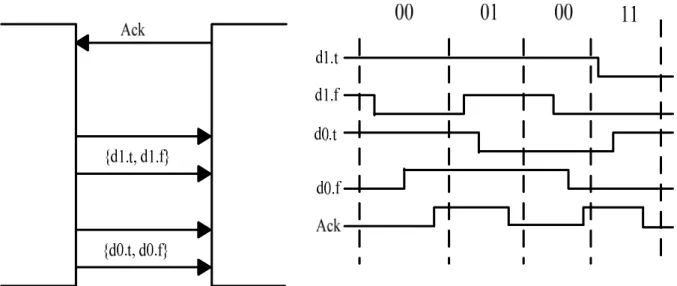
The 2-phase dual-rail protocol also uses 2 wires {d.t, d.f} per bit, but the information is encoded as transitions. The information on the request and acknowledge wires is now encoded as signal transitions on the wires and there is no difference between 0->1 and 1->0 transition, they both represent a signal event. On an N-bit channel a new codeword is received when exactly one wire in each of the N wire pairs has made a transition. There is no empty value. A valid message is acknowledged and followed by another message that is acknowledged. Figure 2-4 shows the signal waveforms on a 2-bit channel using the 2-phase dual-rail protocol.
Figure 2-4: Illustration of the handshaking on a 2-phase dual-rail channel
2.1.2 Classification of Asynchronous Circuits
Asynchronous circuits can be classified into self-timed, speed-independent, quasi-delay-insensitive and delay-insensitive depending on the delay assumptions that are made.
(1) Delay-Insensitive (DI): A circuit that operates “correctly” with positive, bounded but abstract delay in wires as well as in gates. Such circuits are obviously extremely robust. However, there are too many constraints in pure DI circuits that make it hard to implement. Only circuits composed of C-elements and inverters can be delay-insensitive.
(2) Quasi-Delay-Insensitive (QDI): Circuits that are delay-insensitive with the exception
of some carefully identified wire forks where d1 = d2 as figure 2-5 illustrated are called
quasi-delay-insensitive (QDI). Such wire forks where signal transitions occur at the same time at all end-points are called isochronic fork.
1
2
Figure
rectly” with positive, bounded but unknown delay in gates and ideal zero-delay in wires.
orrect operation relies on more elaborate and/or ing assumptions.
2.2 Asynchronous Pipeline
odel we choose, we will introduce the Muller C-element and 4-phase
2.2.1 C-element
2-5: Quasi-Delay Insensitive Delay Model
(3) Speed-Independent (SI): A circuit that operates “cor
(4) Self-Timed: circuits whose c engineering tim
There are several asynchronous pipeline implementation styles have been proposed. One of the most important models is the Muller pipeline. It is built from C-elements and inverters. Another well known circuit is called Micropipelines, which is 2-phase bundled-data protocol, introduced by Ivan Sutherland in his Turing Award Lecture [2]. Other asynchronous pipeline implementations use different circuit design methods to replace the C-element and latch. Because of the m
dual-rail pipeline.
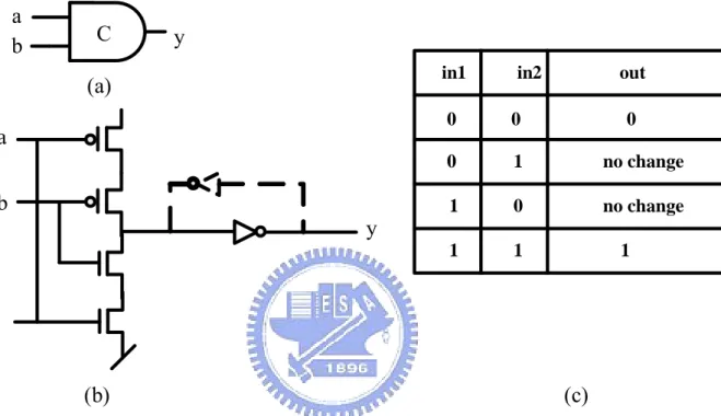
the symbol, construction and truth-table of a two input C-element. When all of the inputs of a C-element are low, the output will be low; when two inputs of a C-element are high, the output will be high; otherwise the output will remain unchanged. With this property, the
etimes can be used as a storage element. C-element som in1 in2 0 0 0 1 0 1 1 1 out 0 no change 1 no change
C
y
a
b
a
y
(a)
(b)
(c)
b
Figure 2-6: C-element: (a) symbol; (b) possible implementation; (c) truth-table
2.2.2 4-phase dual-rail Pipeline
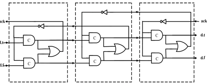
A 4-phase dual-rail pipeline is based on the Muller Pipeline; however the request signal can be eliminated by the dual-rail encoding of data. Figure 2-7 shows the implementation of a 1-bit wide and three-stage pipeline without data processing.
Figure 2-7: A simple 3-stage 1-bit wide 4-phase dual-rail pipeline
To construct circuits with this protocol, gates and data storing elements are required. Each stage can be considered as a dual-rail latch. This latch is used to store the data similar to a master slave flip-flop in a synchronous circuit. In the initial state, each stage is in NULL state (null codeword {d.t, d.f} = {0, 0}) which means the output of C-element in each stage is low. The null data causes acknowledge signal low. After the signal pass through an inverter, one of the input of the C-elements in each stage is high. At this moment, the stage is ready to accept the data codeword {0, 1} or {1, 0}. After receiving a valid data codeword, the acknowledge signal turns to high to indicate the previous stage that it has to accept null data. We should notice that because the codeword {1, 1} is illegal and does not occur, the acknowledge signal generated by the OR gate safely indicates the state of the pipeline stage as “Data” or “Null”.
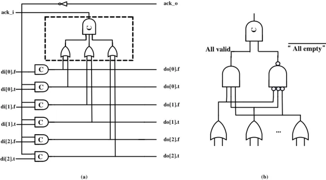
An N-bit wide pipeline can be implemented by using a number of 1-bit pipelines in parallel. If bit-parallel synchronization is needed, the individual acknowledge signals can be combined into one global acknowledge with a C-element. Figure 2-8(a) shows a 3-bit wide latch. The OR gates and the C-element in the dashed box form a “completion detector” that indicates whether the 3-bit dual-rail codeword stored in the latch is valid data or null data. Figure 2-8(b) shows an alternative completion detector that uses only a 2-input C-element.
di[0].f C C C C C C C C C C C C di[0].t di[1].f di[1].t di[2].f di[2].t do[0].f do[0].t do[1].f do[1].t do[2].f do[2].t ack_i ack_o ... C
All valid All empty
(a) (b)
Chapter 3. Analysis and Implementation
3.1 Overview
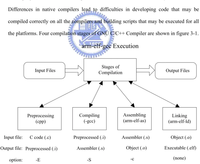
Because we need to know the usages of each instruction in a program, we selected the MediaBench and MiBench as the target programs to be analyzed and compiled them with GNU C/C++ compiler. GNU C/C++ Compiler (GCC) is an integrated distribution of compilers for several major programming languages. These languages currently include C, C++, Java, Fortran, and Ada. GCC is often the compiler chosen for developing software that is required to execute on a wide variety of hardware. Differences in native compilers lead to difficulties in developing code that may be compiled correctly on all the compilers and building scripts that may be executed for all the platforms. Four compilation stages of GNU C/C++ Compiler are shown in figure 3-1.
Input Files CompilationStages of Output Files
Preprocessing (cpp)
Compiling (-gcc)
Assembling
(arm-elf-as) (arm-elf-ld)Linking
Input file: Output file: option: C code (.c) Preprocessed (.i) -E Preprocessed (.i) Assembler (.s) -S Assembler (.s) Object (.o) -c Object (.o) Executable (.elf) (none)
arm-elf-gcc Execution
Preprocessor convert all preprocessing statements such as #define, #include, and #ifdef into true C code. Compiler converts preprocessed input into assembly codes. Assembler takes the assembly codes as input and produces object files with extensions. Linking is the final stage, where the modules are placed in the executable file. Library functions that the program refers to are also placed in the file.
3.2 Result of analysis
In this thesis we use C program codes of MiBench and MediaBench as source and ARM as target processor. “arm-elf” means that target machine is ARM and the supported file format is ELF file format. MiBench and MediaBench are a set of embedded applications for benchmarking. We choose parts of applications as our object of analysis. They includes fft, bitcnts, crc, qsort, and video encoding/decoding which have been proposed as a benchmark representative of multimedia, automotive/industrial control system and communications applications. The purposes of each benchmark are illustrated as follows.
fft: This benchmark performs a Fast Fourier Transform and its inverse transform on an array of data. Fourier transforms are usually used in digital signal processing to find frequencies contained in a given input signal which is a polynomial function with pseudorandom amplitude and frequency sinusoidal components.
bitcnts: The bit count algorithm tests the bit manipulation abilities of a processor by counting the number of bits in an array of integers. The input data is an array of integers with equal numbers of 1’s and 0’s.
crc: This benchmark performs a 32-bit Cyclic Redundancy Check on a file. CRC checks are often used to detect errors in data transmission.
known quick sort algorithm. Sorting of information is important for systems so that priorities can be made, output can be better interpreted, data can be organized, and the overall runtime of programs reduced.
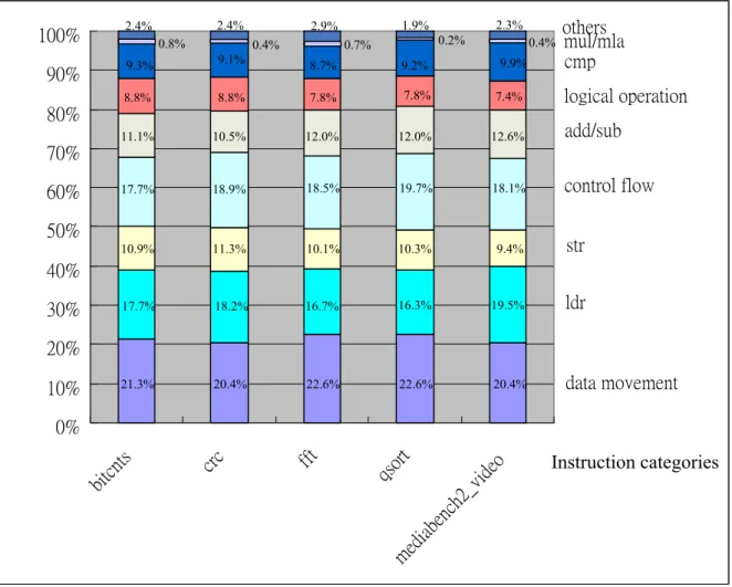
Video encoding/decoding: The video-centric media benchmark suite is composed of the encoders and decoders from video compression standards: H.263, H.264, MEPG-2, and MEPG-4. After compiling, we can obtain the assembly code for following analyzing. Figure 3-2 shows the percentages of each instruction categories.
0% 10% 20% 30% 40% 50% 60% 70% 80% 90% 100% bitcn ts crc fft qsort mediabe nch2 _video others mul/mla cmp logical operation add/sub control flow str ldr data movement 21.3% 17.7% 10.9% 17.7% 8.8% 9.3% 0.8% 2.4% 11.1% Instruction categories 20.4% 18.2% 11.3% 18.9% 10.5% 8.8% 9.1% 0.4% 2.4% 22.6% 16.7% 10.1% 18.5% 12.0% 7.8% 8.7% 0.7% 2.9% 22.6% 16.3% 10.3% 19.7% 12.0% 7.8% 9.2% 0.2% 1.9% 20.4% 19.5% 9.4% 18.1% 12.6% 7.4% 9.9% 0.4% 2.3%
Figure 3-2: The percentages of each instruction categories
We classify all instructions into seven categories including: data movement, load, store, arithmetic operation, logical operation, comparison, and others. Arithmetic operations include add, sub, MLA/mul. Logical operations include and, or, not, logical shift left, and logical shift right. In computing bounded programs, especially those designed for digital signal processing (DSP), multiply-accumulate is a common operation that computes the product of two
numbers and adds that product with an accumulator. The multiply-accumulate operation is called MLA in ARM processors. It’s the same important as MAC instruction in any DSP processors. From table3-1 we can find that the percentage of arithmetic operations, logical operations and MLA/mul instructions is about 19.7%~20.7%. It seems that the ratio is not so high; however considering other instructions such as branch instructions also needs to use arithmetic logic unit in practice. Thus the utilization of ALU is about 40%. On the other hand, ALU usually is the bottleneck of the performance. Therefore, if we improve the performance of ALU, the overall performance can also be easily improved. In synchronous circuit design, the performance is determined by the slowest component. This property makes synchronous circuits design run at worse-case performance. However, in an asynchronous circuit design, the next computation step can be started immediately after the previous step has been completed. There is no need to wait for a transition of the clock signal. This feature potentially leads to a fundamental performance advantage for asynchronous circuit design that increases with the variability in delays associated with these computation steps. Thus in this thesis we introduce the asynchronous circuit design to improve performance of ALU. Figure 3-3 shows the execution sequence of MLA instruction.
The execution sequence of MLA instruction is that source1 multiplies with source2 first and the intermediate result is then added with source3 to generate the final result. Figure 3-4 shows the idea which extends from MLA instruction.
Figure 3-4: The idea which extends from MLA instruction
e think that the operations in the circle can be replaced by other operations to constitute other common use instructions. W
W
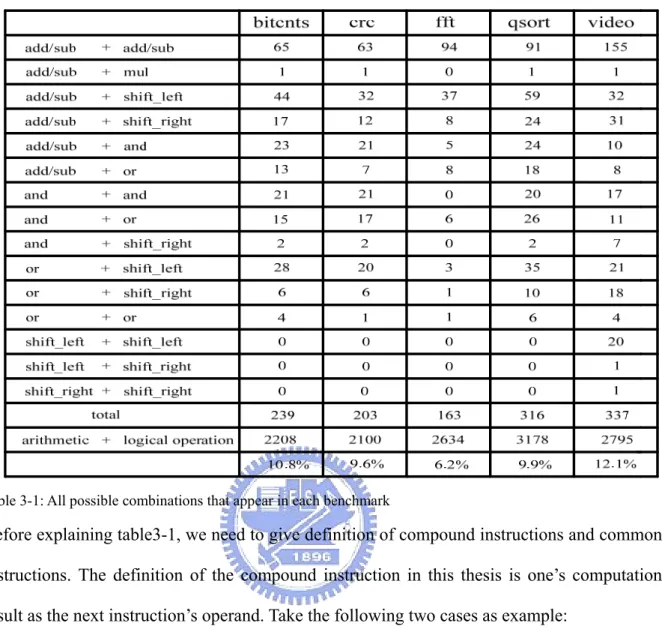
e analyze the assembly code further and find all possible collocations between operations in advance. Table 3-1 shows all possible combinations that appear in each benchmark.
Table 3-1: All possible combinations that appear in each benchmark
Before explaining table3-1, we need to give definition of compound instructions and common instructions. The definition of the compound instruction in this thesis is one’s computation result as the next instruction’s operand. Take the following two cases as example:
case 1: LSL R1, R1, #3
ADD R3, R2, R1 ; R3 := R2 + (R1¯23
)
case 2: ADD R4, R4, #4064 ADD R4, R4, #15
In case 1, the value of register R1 is logical shift left 3-bit and stored into register R1 itself first. Then the intermediate result is added with the value of another register R2 and stored into register R3 finally. In case 2, the value of register R4 is added with the constant value 4046 first. Then the intermediate result is added with the constant value 15 and stored into register R4 itself finally. Because these two cases conform to definition of compound instruction that we just mentioned, we find all these kinds of instructions out from assembly
code. Statistic result is listed in the table 3-1. From table 3-1 we can find that collocations of different operations include: add/sub + add/sub, add/sub + multiply, add/sub + shift left, add/sub + shift right, add/sub + and, add/sub + or, and + and, and + or, and + shift right, or + shift left, or + shift right, or + or, shift left + shift right, shift left + shift left, shift right + shift right. The percentage of these collocations is about 6.2%~12.1% in original arithmetic and logical instructions. Other instructions that contain single operation are called common instructions. Take the following two cases as example:
case 1: ADD R3, R3, #4 (example for arithmetic operation)
case 2: AND R2, R7,R1 (example for logical operation)
The question now is how we can implement an ALU to fulfill the need of compound and common instructions at the same time. One ALU unit can only provide the need of common operation. After collocating two ALU units, the requirements can be satisfied. Figure 3.5 shows process how we transfer our idea illustrated in figure 3.4 to concrete design.
According to the statistic result of table 3-1, we can find operations that can be placed in the circle marked with interrogation point including: add/sub, multiply, and, or, shift left, shift right. Thus each circle was replaced by ALU that includes these operations. Internal structure of each ALU is illustrated in the following section.
3.3 Internal Structure of Proposed ALU
In this section we focus on the explanation of internal structural of the ALU. Figure 3-6 shows diagram of internal structure of the proposed ALU.
Figure 3-6: Block diagram of internal structure of ALU
In synchronous processor design, data path may have several different works depending on the instruction type. Because the clock period is restricted to worst case delay, designer usually do all works in parallel and simply use a multiplexer to select one result to output. However, in DI circuit design it is possible to design circuits that can operate in different length of time and no longer to let data flow through all function blocks. For this reason, the Demux-Demux and Demux-Merge pair is proposed to control the data flow. The 1-bit-select Demux-Merge pair is shown in figure 3-7.
Figure 3-7: 1-bit-select Demux-Merge pair and its implementation
In figure 3-7, the Demux consists of two C-elements. Only one of them will output valid data depending on the select signals. Then the valid data will be sent to only one function block and the other function block will still be NULL. The Merge is composed of OR gate simply. Because only one function block can generate the valid data, it will not influence other unrelated function block and thus the average case delay time is guaranteed. The 1-bit-select Demux-Demux pair is shown in figure3-8.
Figure 3-8: 1-bit-select Demux-Demux pair and its implementation
ontrol signal is 4 bits. The definitions of FnCode are showed in table 3-2.
From figure 3-8 we can find little difference between figure 3-7 and figure 3-8. In figure 3.8 we use sel2.f and sel2.t signals to choose whether bypass another ALU or not. When sel2.t is 1 and sel2.f is 0, computation result of function block is used as one of operand of another ALU. When sel2.t is 0 and sel2.f is 1, the computation result bypasses another ALU as final result. The FnCode is used as sel signal appeared in figure 3-8 and it denotes the operation of an instruction. Because we have 9 operations including 8 operations listed in table 3-2 and bypass, the width of our FnCode c
Table 3-2: The arrangement of FnCode
In addition the definitions of FnCode2 are the same as FnCode1. The purpose of FnCode1 and FnCode2 is used to control ALU. When the FnCode is a value between 0001~1000, it means that ALU will do the corresponding operation listed in table 3-2. For common instruction, the computation result of first ALU is also the final result. For compound instruction, the computation result of first ALU is just one operand of second ALU. For this reason, Demux-Demux is used for the first ALU. Depending on the bypass_or_not signal, the computation result of first ALU will go the right way that it shall go. The bypass_or_not is determined by the following equation:
bypass_or_not = FnCode2 [3] | FnCode2 [2] | FnCode2 [1] | FnCode2 [0]
When FnCode2 [3:0] is 0000, the value of signal bypass_or_not is 0. It means that the computation result will bypass second ALU as the final result. Otherwise the value of signal bypass_or_not is 1. From figure 3-8 we can find that when (sel2.t, sel2.f) = (1, 0) the computation result will go through below path to second ALU as its operand. The advantage of this kind design is its flexibility. We can implement not only common instruction under the
collocation of FnCode1 and bypass but compound instruction under the collocation of FnCode1 and FnCode2. With this design, the instruction type can be designed with high flexibility.
3.4 Implementation
In this section we will introduce the details of implementation. We first introduce the completion detection circuit. How to detect the completion of asynchronous circuits fast is an important issue in asynchronous circuits design because there is no clock distribution. Then we will introduce internal components of ALU in order.
3.4.1 Completion Detection Circuit
Because of the potential advantage of asynchronous design, such as no clock skew problem, low power consumption, average case performance, research of asynchronous logic is increasing [3, 6]. The promise of high performance is especially attractive. To achieve high performance, one must design a fast self-timed circuit with good average case performance and a fast completion detection circuit detecting the completion of the self-timed circuit.
A C-element may be used to implement a completion detection circuit for self-timed or delay-insensitive circuits [7, 9]. Figure 3-9 shows a dual-rail self-timed component with an n-input completion detector. The completion detector consists of an n-input AND gate, an n-input OR gate and a two-input C-element. The n-input AND gate can be regarded as the
computation-completion signal. That is, the computation is done when all Ackis are turned on.
The n-input OR gate can be regarded as the reset-completion signal. That is, the circuit is
are turned off. Therefore the self-timed component has completed an operation when DoneReset signal goes high and it can be reset when DoneReset signal goes down. The completion detector will be used in each self-timed components illustrating in the following section.
Figure 3-9: Self-timed component with completion detection circuit
3.4.2 Logical operation
There are several design methodology to construct the DI circuits, including DIMS[10] and NCL gates[11]. The full name of NCL is NULL Convention Logic. NCL is a symbolically complete logic. It expresses process completely in terms of the logic itself and inherently and conveniently expresses asynchronous digital circuits. NCL is easy to design, but the cost is higher. The thesis is based on the DIMS, and developed with Verilog hardware description language. The full name of DIMS is Delay Insensitive Minterm Synthesis. DIMS is an asynchronous design methodology and the basis for DIMS is the use of two wires to represent each bit of data. This is known as a dual-rail data encoding. The basic elements are modeled in gate level, and all the large blocks are composed of the basic elements.
Figure 3-10: The 2-input dual-rail AND gate
al-rail AND gate. The circuit waits for all its inputs to
3.4.3 Arithmetic operation
In this thesis arithmetic operations include 16*16 bits array multiplier and 32*32 bits carry
Figure 3-10 shows the 2-input du
become valid. When this happens exactly one of the four C-elements goes high. This again causes the relevant output wire to go high corresponding to the gate producing the desired valid output. When all inputs become empty the C-elements are all set low and the output of the dual-rail AND gate becomes empty again. By using the same concepts, other dual-rail basic elements including OR, XOR are constructed. These basic elements are also used to construct the half adder, full adder, and other ALU blocks in hierarchical.
-lookahead adder. We introduce 16*16 bits array multiplier first. Multiplier is an essential device in apparatuses such as microprocessors or in digital signal processors. It also takes the longest operational time, which usually is the decisive factor of an effective chip. For the time being, several asynchronous designs have been proposed. Due to its low power consumption, low average operational time and flexibility to adapt to various process and environment, the asynchronous circuit has been used in VLSI circuits for better performance.
In our design the multiplier comprises a partial product generator, an addition array, a final-stage adder and a completion detector. The partial product generator generates intermediate partial products, and the addition array adds these partial products. Then, the final-stage adder adds these partial products and outputs the sum. Finally, the completion detector checks and output the result. Figure 3.11 shows the work flow of conventional asynchronous multiplier.
Figure 3-11: The work flow of conventional asynchronous multiplier
Figure 3-12 shows an 8*8 bits right-to-left array multiplier including a partial product generator, and a right-to-left addition array.
.
.
.
.
.
.
.
.
.
.
.
.
.
.
.
.
.
.
.
.
.
.
.
.
.
.
.
.
.
.
.
.
.
.
.
.
.
.
.
.
.
.
.
.
.
.
.
.
.
.
.
.
.
.
.
.
.
.
.
.
.
.
.
.
product
Figure 3-12: An 8*8 bits right-to-left array multiplier
In figure 3-12 “●” represents a bit product generation. The partial product generator is usually implemented with an AND gate. ”♁” represents an adder. In the right-to-left array adder, the sum of each adder is propagated to the next-level adder. The carry of each adder is propagated to the higher-bit adder in the same level. The computation result of each adder covered by gray dotted line is used to generate completion-detection signal.
The partial product generator is implemented with the DI AND gate which is illustrated in previous section so that in this section we do not mention it again. Figure 3-13 is a schematic drawing showing a single partial product generator scheme in a single row. Referring to figure 3-13, the gray point represents the partial product, which is the product of multiplier and a particular bit of the multiplicand xj.
Figure 3-13: A conventional single partial product generator scheme
Then the partial products are added by the adder array. In the conventional technique, the DI full adder can be a basic unit of the addition array. To implement the full adder, the dual-rail signal is used for the inputs, (A0, A1), (B0, B1) and (Cin0, Cin1), and the outputs, the sum (S0, S1)
and the carry (Cout0, Cout1). Wherein, the sum and carry can be obtained from the following
logic expressions:
Cout0 = A0 B0 + A0 Cin0 + B0 Cin0
Cout1 = A1 B1 + A1 Cin1 + B1 Cin1
S0 = A0 B0 Cin0 + A1 B1 Cin0 + A0 B1 Cin1 + A1 B0 Cin1
S1 = A1 B1 Cin1 + A1 B0 Cin0 + A0 B1 Cin0 + A0 B0 Cin1
For example, when A = 1, B = 0, and Cin = 1, then Cout = 1 and S = 0. By using dual-rail
encoding, we can use (A0, A1) = (0, 1) to represent A (valid “1”), (B0, B1) = (1, 0) to represent B (valid “0”), and (Cin0, Cin1) = (1, 0) to represent Cin (Valid “1”). After applying to the above
logic expression, we can obtain (Cout0, Cout1) = (0, 1) which represents valid “1” and (S0, S1) =
(1, 0) which represents valid “0”. The result agrees with our expectation. Figure 3-14 is a schematic drawing showing a dual-rail symbol of a DI full adder.
Figure 3-14: A dual-rail symbol of a DI full adder
The DI full adder can be needed to comprise the right-to-left carry-ripple array of the asynchronous multiplier shown in figure 3-13.
After introducing array multiplier, the details of DI Carry-Lookahead Adder are illustrated in the following paragraph. DI Carry-Lookahead Adder can be implemented by using dual-rail signaling in input bits, sum bits, carry bits, and carry-kill bit. A carry is said to be “generated” from a given bit position if the sum for the given position produces a carry out independent of a carry in. A carry is said to be “killed” in a given bit position if a carry does not propagate through the bit. Thus the adder is statistically faster than the ripple adder since carry-kill and carry-generate signals can be generated in the middle bits instead of going through all the carry logic from the least significant bit (LSB). The terms propagate, generate, and kill may be applied to blocks. Several full adders can also be grouped together to form an adder block. A carry is said to propagate through a given block if a carry transferred into the given block’s LSB summation is followed by a carry out of the given block’s MSB summation. A block is said to generate a carry if the block’s MSB summation produces a
carry out, independent of carries into the block’s LSB. Figure 3-15 is a schematic drawing showing a conventional DI carry lookahead adder. The DICLA comprises the input bits (Ai, Bi), the output bits (Si, Ci) and the hot code (ki, gi, pi) of internal signal. For simplicity, we use an 8-bits DICLA scheme as example.
Figure 3-15: An 8*8 bits DICLA scheme
The DICLA can be built with two basic modules: C and D modules, connected in a tree-like structure. The equations of the C module are defined as follows:
Carry-kill ki = Ai0Bi0
Carry-generate gi = Ai1Bi1
Carry-propagate pi = Ai0Bi1 + Ai1Bi0
Sum S0 = A0 B0 Cin0 + A1 B1 Cin0 + A0 B1 Cin1 + A1 B0 Cin1
SumS1 = A1 B1 Cin1 + A1 B0 Cin0 + A0 B1 Ci0 + A0 B0 Ci1
Where i = 0, 1, …, n-2, n-1. The C module is shown in figure 3-16. The dual-rail signals on the left side of figure 3-16 are grouped as Ai = (Ai0, Ai1), Bi = (Bi0, Bi1), Ci = (Ci0, Ci1), Si =
(Si0, Si1), and Ii = (ki, gi, pi). The schematic symbol of C module is shown on the right side of
figure 3-16.
Figure 3-16: C-module
The equations for the D module are defined as follows: Block-carry-propagate Pi,k = Pi,jPj-1,k
Block-carry-kill Ki,k = Ki,j + Pi,jKj-1,k
Block-carry-generate Gi,k = Gi,j + Pi,jGj-1,k
Block-carry-out = Cj0 = Kj-1,k + Pj-1,kCk0
Block-carry-out = Cj1 = Gj-1,k + Pj-1,kCk1
Figure 3-17: D-module
The signals on the left side of figure 3-17 are grouped as Ii,j = (Ki,j, Gi,j, Pi,j), and Ci = (Ci0, Ci1).
The schematic symbol of D module is shown on the right side of figure 3-17. Initially, all carries (Ci0, Ci1 for i = 1, 2, …, n) and the internal signals (Ki,j, Gi,j, Pi,j) are zero, because all
primary inputs (Ai0, Ai1, Bi0, and Bi1 for i = 0, 1, …, n-1) and input carry (Ci0, Ci1) are zero.
During the computation, the inputs Ai0, Ai1, Bi0, Bi1, C00, and C01 become valid, and then the
outputs (Ci0, Ci1) and (Si0, Si1) for i = 1, 2, …, n become valid gradually. Finally, the
completion detector checks all outputs and outputs the completion signal indicating that the operation is completed.
3.4.4 Barrel Shifter
Data shifting and rotating are required in several applications including arithmetic operations, variable-length coding, and bit-indexing. Consequently, barrel shifters which are capable of shifting or rotating data are commonly found in both digital signal processors and general-purpose processors. In this thesis, we define A to be the input operand, B to be the shift/rotate amount, and R to be the shift/rotated result. We define A to be an n-bit value,
where n is an integer power of two. Therefore, B is a log2(n)-bit integer representing values
from 0 to n-1. The barrel shifter performs the following six operations: shift right logical, shift right arithmetic, rotate right, shift left logical, shift left arithmetic, and rotate left. The dual-rail signal is used for the inputs, ai = (ai0, ai1) and bi = (bi0, bi1), and the outputs, ri = (ri0,
ri1) where i = 0, 1, …, n-1. Table 3-3 gives an example for each of these operations. In this
table, the bit vector for A is denoted as a7a6a5a4a3a2a1a0 and the shift/rotate amount, B, is 3
bits.
Table 3-3: Shift and rotate example for A = a7a6a5a4a3a2a1a0 and B = 3
As illustrated in this table:
z A B-bit shift right logical operation performs a B-bit shift and sets the upper B bits of the result to zeros.
z A B-bit shift right arithmetic operation performs a B-bit right shift and sets the upper B bits of the result to an-1, which corresponds to the sign bit of A.
z A B-bit rotate right operation performs a B-bit right shift and sets the upper B bits of result to the lower B bits of A.
z A B-bit shift left logical operations performs a B-bit left shift and sets the lower B bits of the result to zeros.
of the result to zeros. The sign bit of the result is sets to an-1.
z A B-bit rotate left operation performs a B-bit left shift and sets the lower B bits of result to the upper B bits of A.
The operation performed by the barrel shifters is controlled by a 3-bit opcode, which consists of the bits left, rotate, and arithmetic, as summarized in table 3-4.
1
0
rotate left
0
0
0
0
0
1
0
1
0
1
0
0
1
0
1
1
shift right logical
shift left logical
shift right arithmetic
rotate right
shift left arithmetic
rotate
arithmetic
Table 3-4: Operation control bits
Control signals are set to 1 when performing left, rotate, and arithmetic operations
respectively. An n-bit logarithmic barrel shifter uses log2(n) stages. Each bit of the shift
amount, B, controls a different stage of the shifter. The data transferred into the stage controlled by bk is shifted by 2k bits if bk = 1; otherwise it is not shifted. Figure 3-18 shows the
block diagram of an 8-bit logical right shifter, which uses three stages with 4-bit, 2-bit, and 1-bit shifts.
Figure 3-18: The block diagram of an 8-bits logical right shifter
A similar unit that performs right rotations can be designed by modifying the connections to the more significant multiplexers. Figure 3-19 shows the block diagram of an 8-bit right rotator, which uses three stages with 4-bit, 2-bit, and 1-bit rotates. The right rotator and the logical right shifter provide different inputs to the more significant multiplexers.
Interconnect lines are inserted to enable routing of the 2k low order data bits to the 2k high
order multiplexers in the stage controlled by bk. There is no longer need for interconnect lines
Figure 3-19: An 8-bits right rotator
The 1-bit multiplexer is shown in figure 3-20. The left side of figure 3-20 shows the symbol of 1-bit-select multiplexer and right side of figure 3-20 shows its implementation. In figure 3-20, the multiplexer consists of two C-elements and OR gate. Only one of the C-elements will output valid data depending on the select signals. Then the valid data will be merged by OR gate because only one C-element can generate valid data.
The logical right shifter can be extended to also perform shift right arithmetic and rotate right operations by adding additional multiplexers. Figure 3-21 shows an 8-bit right shifter/rotator with three stages of 4-bit, 2-bit, and 1-bit shifts/rotates.
Figure 3-21: An 8-bits right shifter/rotator
When the control signal sra is 1, the right shifter/rotator performs shift right arithmetic operation. When the control signal sra is 0, it performs shift right logical operation. Initially a
single multiplexer selects between 0 for logical right shifting and an-1 for arithmetic right
shifting to produce signal s. In the stage controlled by bk, 2k multiplexers select between
signal s for shifting and the 2k lower bits of the data for rotating. From figure 3-21 we can find that the design concept of right shifter/rotator is composed of logical right shifter, right rotator, and extra multiplexers mentioned earlier. Left shift operations can also use the same concept to implement so we do not need tautology.
Chapter 4. Simulation Results
Because in ALU multiplier usually takes the longest computation time, we pay our attention on the comparison of performance between synchronous and asynchronous circuit design. Figure 4-1 shows a 16*16 bits right-to-left array multiplier.
Figure 4-1: A 16*16 bits right-to-left multiplier
In figure 4-1 the gray dotted line represents the critical path of array multiplier. Furthermore, in order to verify the correctness of the design, ModelSim 6.0 is used. We also tried to synthesis our gate-level design with Design Compiler. The data listed in the table is based on the TSMC 0.13 μm cell library. From the table we can find that the worst case delay for asynchronous array multiplier is 41.223 ns and 18.325 ns for combinational array multiplier. It seems that the performance of synchronous array multiplier is better than asynchronous one. The sentence is not always true because the happening probability of worst case is very low in actual life. Let’s take an instruction MLA in our daily life such as 213 + (216*144) for example. Figure 4-2 shows the waveform of instruction MLA.
Figure 4-2: The waveform of instruction MLA
From the figure we can find that the instruction takes 21.199 ns. Other delays of possible combinations are listed in table 4-1.
Table 4-1: Other delays of possible combinations
numbers such as 144 or 213. For combinational logic, it takes 37.750 ns under two-stage ALU design because multiplier usually takes the longest operational time and bounded to the worst case delay. From here we can find that the performance of asynchronous circuit design in this thesis may be better than synchronous circuit design in this case. It is a feasible way that one applies the advantage of asynchronous circuit designs that operate at average rates instead of worst rates on designing ALU.
Chapter 5. Conclusion
Because ALU usually is the bottleneck of the processor performance, improving the processing time of ALU is also the chance to improve overall performance. In synchronous circuit design, the performance is determined by the slowest component. However, in an asynchronous circuit design, the next computation step can be started immediately after the previous step has been completed. This feature potentially leads to a fundamental performance advantage for asynchronous circuit design, an advantage that increases with the variability in delays associated with these computation steps. Thus in this thesis we introduce the concepts of asynchronous circuit design to improve performance of ALU.
The original idea of this design is derived from MAC instruction in any DSP processors. The MAC instruction is an operation that computes the product of two numbers and adds that product with an accumulator. Then we extend this idea to design our ALU composed of two stages. The advantage of this kind of design is its flexibility on instruction types and delays. We can implement not only common instruction under the collocation of FnCode1 and bypass but compound instruction under the collocation of FnCode1 and FnCode2. With this design, the instruction type can be designed with high flexibility. In addition, the property of data dependency can also make the variability in delays more flexible in asynchronous circuit design and verified by the final simulation results in chapter 4.
Reference
[1] J. SparsØ and S. Furber, Principles of asynchronous circuit design – a systems prospective, Kluwer Academic Publishers, London, 2001.
[2] I. Sutherland, “Micropipelines,” Communications of the ACM, vol. 32, June 1989, pp. 20-38.
[3] Al Davis and Steven M. Nowick, “Asynchronous circuit design: Motivation, background, and methods,” in Asynchronous Digital Circuit Design, Workshops in Computing, 1995, pp.1-49.
[4] Mark E. Dean, David L. Dill, and Mark Horowitz, “Self-timed logic using current-sensing completion detection,” in Journal of VLSI Signal Processing, February 1994, pp. 7-16.
[5] E. Grass, R. C. S. Morling, and I. Kale, “Activity monitoring completion detection: A new single rail approach to achieve self-timing,” Proc. International Symposium on Advanced Research in Asynchronous Circuits and Systems, March 1996.
[6] Scott Hauck, “Asynchronous design methodologies: An overview,” Proceedings of the IEEE, January 1995.
[7] Fu-Chiung Cheng, “Synthesis of high speed delay-insensitive combinational iterative tree circuits,” in Proc. International Conf. Computer Design, October 1997, pp. 301-306.
[8] Fu-Chiung Cheng, Stephen H. Unger, Michael Theobald, and Wen-Chung Cho, “Delay-insensitive carry-lookahead adders,” in Proc. International Conf. VLSI Design, 1997, pp. 322-328.
[9] Ilana David, Ran Ginosar, and Michael Yoeli, “An efficient implementation of Boolean functions as self-timed circuits,” IEEE Transactions on Computers, January 1992, pp. 2-11 [10] G. E. Sobelman and K. Fant, “CMOS circuit design of threshold gates with hysteresis,” in Proc. IEEE Symp. Circuits and Systems, vol. 2, 1998, pp. 61-64.
[11] D. Muller and W. Bartky, “A Theory of asynchronous circuits,” in Proceeding of an International Symposium on the Theory of Switching, April 1959, pp. 204-243.