Characteristics of Self-Aligned Si/Ge T-Gate
Poly-Si Thin-Film Transistors With
High
ON
/
OFF
Current Ratio
Po-Yi Kuo, Tien-Sheng Chao, Senior Member, IEEE, Pei-Shan Hsieh, and Tan-Fu Lei, Member, IEEE
Abstract—In this paper, we have successfully developed and
fabricated self-aligned Si/Ge T-gate poly-Si thin-film transistors (Si/Ge T-gate TFTs) with a thick gate oxide at the gate edges near the source and drain for the first time. The Si/Ge T-gate was formed by selective wet etching of Ge gate layer. The thick gate oxide layer at the gate edges and passivation oxide layer were deposited simultaneously in passivation process. The thick gate oxide at the gate edges effectively reduces the drain vertical and lateral electric fields without additional mask, lightly doped drain, spacer, or subgate bias. The Si/Ge T-gate TFTs not only reduce theOFF-state leakage current but also maintain a highON-state current. Experimental results show that the Si/Ge T-gate TFTs have low OFF-state leakage currents, improved ON/OFF current ratio, and more saturated output characteristics compared with conventional TFTs.
Index Terms—Germanium, ON/OFF current ratio, polycrys-talline silicon thin-film transistors (poly-Si TFTs), self-aligned, Si/Ge T-gate.
I. INTRODUCTION
P
OLYCRYSTALLINE silicon thin-film transistors (poly-Si TFTs) have been widely used in many potential appli-cations including high-density flash memories, active-matrix organic light emitting diode, and active-matrix liquid crystal displays [1]–[4]. Poly-Si TFTs are considered to be promising devices for display system-on-panel applications [5]. However, the large OFF-state leakage current and device instability of poly-Si TFTs are hindrances to the performance and high-reliability circuit applications. It is well known that the dom-inant mechanism of the OFF-state leakage current is the field emission via grain boundary traps due to a high electric field in the drain depletion region. The leakage current is increased with increasing gate and drain voltages which enhance the field emission via grain boundary traps in the depletion region near the drain [6], [7]. In order to increase the reliability and reduce the leakage current, poly-Si TFTs with offset gated, lightlyManuscript received October 25, 2006; revised February 12, 2007. This work is supported by the National Science Council, Taiwan, R.O.C., under Contract NSC-95-2221-E-009-279. The review of this paper was arranged by Editor V. R. Rao.
P.-Y. Kuo and T.-F. Lei are with the Department of Electronics Engineering and Institute of Electronics, National Chiao Tung University, Hsinchu 300, Taiwan, R.O.C.
T.-S. Chao and P.-S. Hsieh are with the Department of Electrophysics, National Chiao Tung University, Hsinchu 300, Taiwan, R.O.C.
Color versions of one or more of the figures in this paper are available online at http://ieeexplore.ieee.org.
Digital Object Identifier 10.1109/TED.2007.894604
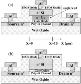
Fig. 1. Schematic cross-sectional device structures of (a) Si/Ge T-gate TFTs and (b) conventional TFTs.
doped drain (LDD), gate-overlapped LDD, floating gate spacer, air cavity, or field-induced drain (FID) structures have been suggested to reduce the electric field near the drain [8]–[14].
In this paper, a novel self-aligned Si/Ge T-gate poly-Si TFT is proposed and demonstrated. The Si/Ge T-gate was formed by selective wet etching of Ge gate layer. The Ge regions etched at the gate edges were refilled by low-pressure chemical vapor deposition tetraethoxysilane (LPCVD TEOS) oxide in the pas-sivation process. The thick gate oxide layer at the gate edges and the passivation oxide layer were deposited simultaneously in the passivation process. The thick gate oxide at the gate edges effectively reduces the drain vertical and lateral electric fields without additional mask, LDD, spacer, and subgate bias. The lateral electric field within the channel can be lowered by using the lateral selective etching of Ge within the gate stack at the gate edges without extra fabrication cost in the Si/Ge T-gate TFTs. The Si/Ge T-gate TFTs have a reducedOFF-state leakage current at negative voltages, an improvedON/OFFcurrent ratio, and a smaller drain conductance in saturation due to a reduced impact ionization at the drain end of the channel compared with conventional TFTs.
II. DEVICESTRUCTURE ANDDESIGN
Fig. 1 shows the schematic cross-sectional device structures of [Fig. 1(a)] Si/Ge T-gate TFTs and [Fig. 1(b)] conventional
TFTs. Both devices have the same photomask gate length and perform the same source/drain (S/D) implantation condition. The experimental split table of Si/Ge T-gate TFTs and con-ventional TFTs is defined in Table I. In Si/Ge T-gate TFTs, the thickness of the thick gate oxide layer at the gate edges is controlled by the thickness of Ge gate layer (50 and 100 nm), and the Ge lateral undercut distances (400 and 800 nm) are controlled by the time of selective wet etching. For example, the Si/Ge50 nm T-gate TFTs (400 nm) have a 150-nm/50-nm stacked Si/Ge gate layer and a 400-nm Ge lateral undercut distance. The total thickness of stacked Si/Ge gate layer is 200 nm for all devices.
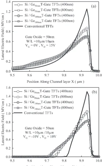
The Si/Ge T-gate TFTs can reduce the vertical electric field near the drain due to the thick gate oxide layer at the gate edges [12]. The poly-Si region under thick gate oxide can be considered as an offset region, and the gate edge over the thick gate oxide serves as a field plate connected with the gate so that the proposed TFTs operate like FID TFTs except a subgate bias [13]. In the OFF-state, the lateral electric field near the drain can be reduced due to the thick gate oxide layer at the gate edges [12]. In theON-state, a sufficient inversion layer can be induced by the thick gate-edge oxide near the source [14]. In order to demonstrate the reduction in drain lateral electric field in the Si/Ge T-gate TFTs, the electric fields in the TFTs were simulated by using a commercial 2-D numerical simu-lator for semiconductor devices. Fig. 2 shows the simulated lateral electric field distribution along the channel/gate oxide interface for conventional TFTs and Si/Ge T-gate TFTs with applied biases at [Fig. 2(a)] VG= 0 V and VD= 15 V, and at [Fig. 2(b)] VG =−10 V and VD= 10 V. The simulated result demonstrates that lateral electric field near the drain can be effectively reduced by the Si/Ge T-gate structure. The Si/Ge T-gate TFTs with 100-nm Ge gate layer have the lowest lateral electric field near the drain due to the thickest gate oxide at the gate edges [12].
III. EXPERIMENT
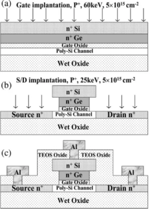
Fig. 3 shows the main fabrication process steps of Si/Ge T-gate TFTs. First, a 100-nm amorphous silicon (a-Si) layer was deposited by LPCVD at 550◦C on oxidized silicon wafers and then was crystallized by solid phase crystallization at
Fig. 2. Simulated lateral electric field distribution along the channel/gate oxide interface for conventional TFTs and Si/Ge T-gate TFTs with applied biases at (a) VG= 0 V and VD= 15 V and at (b) VG=−10 V and
VD= 10 V.
600 ◦C for 24 h. After the patterning of the active region, a 50-nm TEOS gate oxide layer was deposited by LPCVD. Subsequently, a stacked a-Si/a-Ge gate layer was deposited by LPCVD at 550◦C/370◦C. The thickness of the thick gate oxide layer at the gate edges was controlled by the thickness of the Ge gate layer (50 and 100 nm). A phosphorus gate implantation with dose 5× 1015cm−2and energy 60 keV was used to form the n+−gate [Fig. 3(a)]. After defining the gate electrode, the Si/Ge T-gate was formed by selective wet etching (H2O : H2O2 solution) of Ge gate layer at 75 ◦C. The Ge lateral undercut distances (400 and 800 nm) of Si/Ge T-gate were controlled by the time of wet etching. Then, the remaining oxide on the S/D region was removed by diluted HF. A self-aligned phosphorus implantation with dose 5× 1015cm−2and energy 25 keV was used to form the n+ S/D [Fig. 3(b)]. The Ge undercut regions were refilled by LPCVD TEOS oxide in the passivation process, and dopants were activated by furnace at 600◦C for 12 h. After contact and metallization processes [Fig. 3(c)], NH3 plasma treatments were implemented after sintering at 400 ◦C for 30 min. Conventional TFTs with self-aligned n+S/D and TEOS passivation were also fabricated to serve as control ones.
Fig. 3. Main fabrication process steps of Si/Ge T-gate TFTs.
Fig. 4. Cross-sectional TEM microphotograph of Si/Ge T-gate TFTs.
IV. RESULTS ANDDISCUSSION
Fig. 4 shows the cross-sectional transmission electron mi-croscopy (TEM) microphotograph of Si/Ge T-gate TFTs. The Si/Ge T-gate was successfully obtained on the gate oxide, and the interfacial oxide was not observed in the stacked Si/Ge interface. The Si and Ge gate layers were interalloyed between the stacked Si/Ge interface due to subsequent processes anneal-ing. The undercut regions were fully refilled by LPCVD TEOS oxide in the passivation process, and the thickness of thick gate oxide at the gate edges was controlled by the thickness of the Ge gate layer. In Fig. 4, the thickness of the Ge gate layer is about 100 nm, and the Ge lateral undercut distance of Si/Ge T-gate is about 400 nm. The poly-Si at the gate edges was bent upward by subsequent process-induced thermal stresses. The bending poly-Si at the gate edges brings about gradual variation in the thickness of the gate oxide at the gate edges, and the thickest gate oxide is near the drain. The vertical and lateral electric fields at the drain can be effectively reduced by a thick gate
Fig. 5. Composition of pure Ge gate layer extracted from the energy disper-sive X-ray spectrometer analysis.
oxide at the gate edges. In addition, the bending poly-Si at the gate edges can promote the refilling ability of LPCVD TEOS. Fig. 5 illustrates the composition of pure Ge gate layer extracted from the energy dispersive X-ray spectrometer analysis. The pure Ge gate layer of Si/Ge T-gate can be easily etched by the wet etching H2O : H2O2(100 : 1) solution at a low temperature of 75◦C. The etching rate is about 2.5 nm/s.
Fig. 6 exhibits the measured transfer characteristics of con-ventional TFTs and Si/Ge T-gate TFTs with [Fig. 6(a)] W/L = 10 µm/10 µm and [Fig. 6(b)] W/L = 10 µm/5 µm. TheOFF -state leakage currents of Si/Ge T-gate TFTs are significantly lower than those of conventional TFTs. This is because the lateral electric field near the drain can be effectively reduced by the Si/Ge T-gate structure. Since the thick gate oxide at the gate edges greatly suppresses the lateral drain electric field, the anomalousOFF-state leakage currents of poly-Si TFTs can be controlled by the thickness of the Ge gate layer and the Ge lateral undercut distances [14]. The Si/Ge100 nm T-gate (800 nm) TFTs have the lowestOFF-state leakage currents in the Si/Ge T-gate TFTs. TheON-state currents of Si/Ge T-gate TFTs are slightly lower than those of conventional TFTs. A sufficient inversion layer can be induced by the thick gate-edge oxide near the source. For the Si/Ge T-gate TFTs, theON-state currents are slightly reduced with increasing thickness of Ge gate layer and Ge lateral undercut distances. The Si/Ge50 nmT-gate (400 nm) TFTs have the highest ON-state currents among all the Si/Ge T-gate TFTs.
Fig. 7 displays the measured OFF-state leakage currents of conventional TFTs and Si/Ge T-gate TFTs with W/L = 10 µm/10 µm for different drain biases at VG=−10 V. The
OFF-state leakage currents of Si/Ge T-gate TFTs are signifi-cantly lower than those of conventional TFTs. The OFF-state leakage current is increased with increasing gate and drain voltages which enhance the field emission via grain boundary traps in the depletion region near the drain [6], [7]. In the Si/Ge T-gate TFTs, the lateral electric field near the drain can be greatly reduced due to the thick gate oxide layer at the gate edges, and theOFF-state leakage currents are greatly decreased with increasing thickness of the Ge gate layer and the Ge lateral undercut distances.
Fig. 6. Measured transfer characteristics of conventional TFTs and Si/Ge T-gate TFTs with (a) W/L = 10 µm/10 µm and (b) W/L = 10 µm/5 µm.
Fig. 7. Measured OFF-state leakage currents of conventional TFTs and Si/Ge T-gate TFTs with W/L = 10 µm/10 µm for different drain biases at
VG=−10 V.
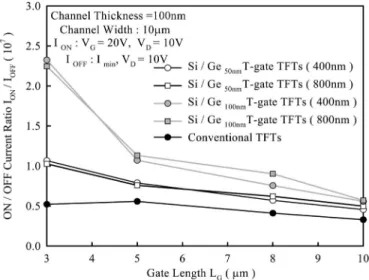
Fig. 8 illustrates the measuredON/OFFcurrent ratio of con-ventional TFTs and Si/Ge T-gate TFTs with W = 10 µm and different channel length. TheON/OFFcurrent ratio is defined as
Fig. 8. MeasuredON/OFFcurrent ratio of conventional TFTs and Si/Ge T-gate TFTs with W = 10 m and different channel length. TheON/OFFcurrent ratio is defined as the ratio of theON-state current to the minimumOFF-state leakage current. TheON-state current is defined as drain–current (ID) at VG= 20 V
and VDS= 10 V, and the minimum OFF-state leakage current is defined as minimum drain–current (Imin) at VDS= 10 V.
the ratio of theON-state current to the minimumOFF-state leak-age current. The ON-state current is defined as drain–current (ID) at VG= 20 V and VDS= 10 V, and the minimum OFF -state leakage current is defined as the minimum drain–current (Imin) at VDS= 10 V. The Si/Ge T-gate TFTs not only reduce theOFF-state leakage current but also maintain a highON-state current. The Si/Ge T-gate TFTs with 100-nm Ge gate layer have the highestON/OFFcurrent ratio than those with 50-nm Ge gate layer due to the lowestOFF-state leakage currents. On the other hand, the Si/Ge T-gate TFTs with 100-nm Ge gate layer can maintain a high ON-state current even though the gate length is scaled down to 3 µm. Hence, to optimize the Si/Ge T-gate TFTs, the thickness of Ge gate layer should be considered first. The Si/Ge T-gate TFTs are different from conventional FID TFTs. The conventional FID TFTs need an additional subgate electrode, a large subgate bias, and an additional subgate mask compared with Si/Ge T-gate TFTs. In addition, the conventional FID TFTs have the farther separation of n+ S/D junction compared with conventional TFTs. In the conventional FID TFTs with a SiO2interlayer, a typical subgate bias of more than 60 V is necessary to obtain a highON/OFFcurrent ratio [13]. The Si/Ge T-gate TFTs and conventional TFTs were fabricated with the same photomask gate length and the same S/D im-plantation condition. The Si/Ge T-gate TFTs and conventional TFTs have the identical position of S/D junction. The Si/Ge T-gate TFTs only need one gate electrode to obtain a high
ON/OFFcurrent ratio.
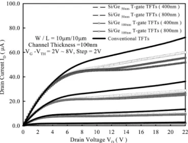
The output characteristics of conventional TFTs and Si/Ge T-gate TFTs with W/L = 10 µm/10 µm are shown in Fig. 9. The Si/Ge T-gate TFTs have more saturated output character-istics compared with conventional TFTs. The kink current of Si/Ge T-gate TFTs is reduced considerably compared with that of conventional TFTs. The Si/Ge T-gate TFTs with 100-nm Ge gate layer have the most saturated output characteristics due to the lowest lateral electric field near the drain. The output
Fig. 9. Output characteristics of conventional TFTs and Si/Ge T-gate TFTs with W/L = 10 µm/10 µm.
characteristics exhibit an anomalous increase of current in the saturation regime, often called “kink” effect due to an analogy with silicon-on-insulator devices [15]–[17]. This phenomenon can be attributed to the floating-body effect [18] and the avalanche multiplication enhanced by grain boundary traps [16], particularly in n-channel TFTs. With increasing drain voltage, the added drain–current enhances impact ionization and parasitic bipolar junction transistor effect, which leads to a premature breakdown in return [18], [19]. Since the Si/Ge T-gate TFTs can reduce the vertical and lateral electric fields near the drain due to the thick gate oxide layer at the gate edges and the poly-Si region under thick gate oxide can be considered as an offset region [12], the impact ionization can be effectively reduced, and the avalanche multiplication enhanced by grain boundary traps can be suppressed by the Si/Ge T-gate TFTs [9]–[11].
V. CONCLUSION
In this paper, a self-aligned Si/Ge T-gate poly-Si TFTs ef-fectively reduce theOFF-state leakage current while still main-taining theON-state current compared with conventional TFTs. The stacked Si/Ge gate layers were successfully deposited by LPCVD. The thick gate oxide layer at the gate edges and passi-vation oxide layer were deposited simultaneously in passipassi-vation process. The thick gate oxide at the gate edges effectively reduces the vertical and lateral electric fields near the drain without additional mask, LDD, spacer, or subgate bias. The Si/Ge T-gate poly-Si TFTs are proved to be a very promising structure with lowOFF-state leakage current, improvedON/OFF
current ratio, and saturated output characteristics for display system-on-panel applications.
ACKNOWLEDGMENT
The authors would like to thank the Nano Facility Center, National Chiao Tung University, and the National Nano Device Laboratory for providing process equipment.
REFERENCES
[1] A. J. Walker, S. Nallamothu, E. H. Chen, M. Mahajani, S. B. Herner, M. Clark, J. M. Cleeves, S. V. Dunton, V. L. Eckert, J. Gu, S. Hu, J. Knall, M. Konevecki, C. Petti, S. Radigan, U. Raghuram, J. Vienna, and M. A. Vyvoda, “3D TFT-SONOS memory cell for ultra-high density file storage applications,” in VLSI Symp. Tech. Dig., 2003, pp. 29–30. [2] T. Shimoda, H. Ohshima, S. Miyashita, M. Kimura, T. Ozawa,
I. Yudasaka, H. Kobayashi, R. H. Friend, J. H. Burroughes, and C. R. Towns, “High resolution light emitting polymer display driven by low temperature polysilicon thin film transistor with integrated driver,” in Proc. ASID, Seoul, Korea, 1998, pp. 217–220.
[3] A. G. Lewis, I.-W. Wu, T. Y. Huang, A. Chiang, and R. H. Bruce, “Active matrix liquid crystal display design using low and high tempe-rature processed polysilicon TFTs,” in IEDM Tech. Dig., San Francisco, CA, 1990, pp. 843–846.
[4] H. Oshima and S. Morozumi, “Feature trends for TFT integrated circuits on glass substrates,” in IEDM Tech. Dig., Washington, DC, 1989, p. 157. [5] K. Werner, “The flowering of flat display,” IEEE Spectr., vol. 34, no. 5,
pp. 40–49, May 1997.
[6] J. G. Fossum, A. O. Conde, H. Shichijo, and S. K. Banerjee, “Anomalous leakage current in LPCVD polysilicon MOSFET’s,” IEEE Trans. Electron
Devices, vol. ED-32, no. 9, pp. 1878–1884, Sep. 1985.
[7] K. R. Olasupo and M. K. Hatalis, “Leakage current mechanism in sub-micron polysilicon thin-film transistors,” IEEE Trans. Electron Devices, vol. 43, no. 8, pp. 1218–1223, Aug. 1996.
[8] Z. Xiong, H. Liu, C. Zhu, and J. K. O. Sin, “Characteristics of
high-κ spacer offset-gated polysilicon TFTs,” IEEE Trans. Electron Devices,
vol. 51, no. 8, pp. 1304–1308, Aug. 2004.
[9] C. T. Liu, C. H. D. Yu, A. Kornblit, and K. H. Lee, “Inverted thin-film transistor with a simple self-aligned lightly doped drain structure,” IEEE
Trans. Electron Devices, vol. 39, no. 12, pp. 2803–2809, Dec. 1992.
[10] M. Hatano, H. Akimoto, and T. Sakai, “A novel self-aligned gate-overlapped LDD poly-Si TFT with high reliability and performance,” in
IEDM Tech. Dig., Washington, DC, 1997, pp. 523–526.
[11] T. Zhao, M. Cao, J. D. Plummer, and K. C. Saraswat, “A novel floating gate spacer polysilicon TFT,” in IEDM Tech. Dig., Washington, DC, 1993, pp. 393–396.
[12] M. C. Lee, S. H. Jung, I. H. Song, and M. K. Han, “A new poly-Si TFT structure with air cavities at the gate-oxide edges,” IEEE Trans. Electron
Devices, vol. 22, no. 11, pp. 539–541, Nov. 2001.
[13] K. Tanaka, K. Nakazawa, S. Suyama, and K. Kato, “Characteristics of field-induced-drain (FID) poly-Si TFT’s with high ON/OFF current ratio,”
IEEE Trans. Electron Devices, vol. 39, no. 4, pp. 916–920, Apr. 1992.
[14] J. Park and O. Kim, “A novel self-aligned poly-Si TFT with field-induced drain formed by the Damascene process,” IEEE Electron Device Lett., vol. 26, no. 4, pp. 249–251, Apr. 2005.
[15] M. Koyanagi, H. Kurino, T. Hashimoto, H. Mori, K. Hata, Y. Hiruma, T. Fujimori, I.-W. Wu, and A. G. Lewis, “Relation between hot-carrier light emission and kink-effect in poly-Si thin film transistors,” in IEDM
Tech. Dig., Washington, DC, 1991, pp. 571–574.
[16] M. Hack and A. G. Lewis, “Avalanche-induced effects in polysilicon thin-film transistors,” IEEE Electron Device Lett., vol. 12, no. 5, pp. 203–205, May 1990.
[17] J. P. Colinge, “Reduction of kink effect in thin-film SOI MOSFETs,”
IEEE Electron Device Lett., vol. 9, no. 2, pp. 97–99, May 1988.
[18] M. Valdinoci, L. Colalongo, G. Baccarani, G. Fortunato, A. Pecora, and I. Policicchio, “Floating body effects in polysilicon thin-film transistors,”
IEEE Trans. Electron Devices, vol. 44, no. 12, pp. 2234–2241, Dec. 1997.
[19] M. C. Lee and M. K. Han, “Poly-Si TFTs with asymmetric dual-gate for kink current reduction,” IEEE Electron Device Lett., vol. 25, no. 1, pp. 25–27, Jan. 2004.
Po-Yi Kuo was born in Pingtung, Taiwan, R.O.C.,
in 1978. He received the B.S. degree in electrical engineering from Feng-Chia University, Taichung, Taiwan, in 2000 and the M.S. degree in electronics engineering from National Chiao Tung University, Hsinchu, Taiwan, in 2002. He is currently working toward the Ph.D. degree at the Institute of Electron-ics, National Chiao Tung University.
His current research topic is the fabrication and characterization of fully Ni-salicided source/drain and gate poly-Si thin-film transistors (TFT) and Si/Ge T-gate poly-Si TFTs.
National Chiao Tung University, Hsinchu, Taiwan, in 1992.
He joined the National Nano Device Laboratories as an Associate Researcher in July 1992 and became a Researcher in 1996. He was engaged in developing the thin dielectrics preparations, cleaning processes, and CMOS device fabrication. He has been with the Department of Electrophysics, National Chiao Tung University, since 2001. He has published more than 100 papers.
Pei-Shan Hsieh was born in Taichung, Taiwan,
R.O.C., in 1982. She received the M.S. degree from Electrophysics Department, National Chiao Tung University, Hsinchu, Taiwan, in 2005.
Her current research interest is in the fabrication process of low-temperature poly-Si TFTs. She is currently in the Electrophysics Department, National Chiao Tung University.
Kung University, Tainan, Taiwan, in 1967, and the M.S. and Ph.D. degrees in electronics engineer-ing from National Chiao Tung University, Hsinchu, Taiwan, in 1970 and 1979, respectively.
From 1970 to 1972, he was with the Fine Prod-ucts Microelectronics Corporation, Taiwan, as an Engineer working on the fabrication of small-signal transistors. From 1980 to 1982, he was the Plant Manager with Photronic Corporation, Taiwan. In 1983, he was with the faculty at National Chiao Tung University as an Associate Professor in the Department of Electronics Engineering and the Institute of Electronics. From 1984 to 1986, he was the Director of the Semiconductor Research Center. During 1991 to 1998, he also was the Deputy Director of the National Nano Device Laboratories. Currently, he is a Professor in the Department of Electronics En-gineering and the Institute of Electronics, National Chiao Tung University. His research interests are semiconductor devices and very large-scale integration technologies.