Effect of bismuth content on the properties of Sr 0.8 Bi x Ta 1.2 Nb 0.9 O 9+y
ferroelectric thin films
Huei-Mei Tsai, Pang Lin, and Tseung-Yuen Tseng
Citation: Journal of Applied Physics 85, 1095 (1999); doi: 10.1063/1.369234 View online: http://dx.doi.org/10.1063/1.369234
View Table of Contents: http://scitation.aip.org/content/aip/journal/jap/85/2?ver=pdfcov
Published by the AIP Publishing
Articles you may be interested in
Degradation and recovery of polarization under synchrotron x rays in Sr Bi 2 Ta 2 O 9 ferroelectric capacitors
J. Appl. Phys. 97, 044106 (2005); 10.1063/1.1851598
Heat-treatment-induced ferroelectric fatigue of Pt/Sr 1x Bi 2+y Ta 2 O 9 / Pt thin-film capacitors
Appl. Phys. Lett. 81, 1477 (2002); 10.1063/1.1502010
Improvement in ferroelectric properties of SrBi 2 Ta 2 O 9 thin films with Bi 2 O 3 buffer layers by liquid-delivery metalorganic chemical-vapor deposition
Appl. Phys. Lett. 79, 1519 (2001); 10.1063/1.1400077
Stress effects of the inter-level dielectric layer on the ferroelectric performance of integrated SrBi 2 Ta 2 O 9 capacitors
J. Appl. Phys. 89, 8011 (2001); 10.1063/1.1371277
Compositional dependence of electrical characteristics of SrBi 2 (Ta 1x Nb x ) 2 O 9 thin-film capacitors
J. Appl. Phys. 84, 6788 (1998); 10.1063/1.369010
Effect of bismuth content on the properties of Sr
0.8Bi
xTa
1.2Nb
0.9O
91yferroelectric thin films
Huei-Mei Tsai,a)Pang Lin,a)and Tseung-Yuen Tsengb)
National Chiao-Tung University, Hsinchu, Taiwan, Republic of China
~Received 28 July 1998; accepted for publication 14 October 1998!
This study investigates the effect of bismuth content on the ferroelectric properties of Sr0.8BixTa1.2Nb0.9O91y ~SBTN, x51.7, 2.0, 2.5, 2.7, 2.9, and 3.2! thin film capacitors. SBTN films
are in situ grown on Pt/SiO2/Si substrates by using two-target off-axis radio-frequency magnetron
sputtering at a substrate temperature of 600 °C. The films are crystallized with a high ~115! diffraction intensity and exhibit a columnar microstructure. Experimental results indicate that the root mean square surface roughness of the film increases with an increase of the bismuth content. In addition, the ferroelectric properties of the films heavily rely on the bismuth content. Moreover, the 440-nm-thick Sr0.8Bi2.5Ta1.2Nb0.9O91yfilms exhibit maximum remanent polarization~2Pr! of 52
mC/cm2 and minimum coercive field ~2Ec! of 28 kV/cm at an applied voltage of 1.5 V. X-ray photoelectron spectral studies reveal that except for Bi13, no lower valence state bismuth exists in the Sr0.8Bi2.5Ta1.2Nb0.9O91yfilm and bismuth substituted in the strontium site still remains in its13
valence state. © 1999 American Institute of Physics. @S0021-8979~99!06302-1#
I. INTRODUCTION
Ferroelectric nonvolatile memory devices have received increasing attention from the perspective of the next genera-tion of highly integrated circuits. A convengenera-tionally used ferroelectric material is lead zirconate titanate ~PZT!.1,2 However, PZT memories with Pt electrodes suffer from fa-tigue, in which the switchable polarization declines at around 108 read/write cycles. Bismuth oxide layered ferroelectric materials based on SrBi2Ta2O9 ~SBT! or SrBi2Nb2O9
~SBN!3–8 have become increasingly important because the
films exhibit no fatigue up to 1012cycles, and have excellent retention characteristics and a low leakage current on Pt elec-trodes. The general formula for the Bi containing layer-type compounds is Bi2An21BnO3n13, where A denotes the 12-fold coordinated cation in the perovskite sublattice, B repre-sents the octahedral site and the bismuth forms the rock-salt type interlayer ~Bi2O2!12 between the perovskite blocks
~An21BnO3n11), and n is the number of octahedral layers
within the perovskite sublattice of the structure. For the sto-ichiometric SrBi2Ta2O9 (n52) compound, there is one
complete perovskite sublattice created by the Ta–O octahe-dra in which a 12-fold A cation ~i.e., Sr! may reside. Osaka et al.9studied the phase transition process of SBT thin films prepared by chemical liquid deposition. A fluorite phase ini-tially formed at a low temperature and it transforms into bismuth-layer-structure family or a pyrochlore phase (x
,1.2 SrBixTa2O9) after 750 °C treatment. Although the
bis-muth content heavily influences remanent polarization~2Pr!, particularly when Sr is deficient, formation of the bismuth layer structure is independent of the bismuth content ~x
51.6–3.0 for SrBixTa2O9). 10,11
It was considered that Sr de-ficiency was compensated by excess Bi12 owing to the fact that the Bi and Sr ionic radii are nearly identical~Sr1251.4 Å, Bi1351.3 Å!. In addition, if the bismuth valence state is
13, maintaining electrical neutrality would lead to some
de-fect formation in the lattice. Therefore, it shifts the Ta posi-tion in the perovskite blocks, and gives rise to permanent electric dipoles. When Sr is in stoichiometry, excess bismuth exists in~Bi2O2)12 rock salt layer, not in perovskite lattice. Therefore, although its influence on electric dipoles in per-ovskite blocks is not significant, it facilitates the grain growth. Both changing the perovskite structure and facilitat-ing the grain growth, caused by the excess bismuth, are es-sential in controlling the ferroelectric properties. Therefore, investigating bismuth content dependence of ferroelectric properties promises means of optimizing the sputtered film preparation process, because the Bi content in the films nor-mally deviates strikingly from that of the target at a high deposition temperature.13–16In this work, we employ a two target off-axis magnetron sputter deposition process to pre-pare SBTN films containing various amounts of bismuth. The microstructure, electrical properties, and x-ray photo-electron spectra of SBTN thin films are thoroughly studied as well.
II. EXPERIMENT
The SBTN films were deposited on a Pt~150 nm!/ SiO2
~250 nm!/Si~100! substrates by simultaneous magnetron
sputtering from two different sintered targets of Sr0.8Bi2.2Ta1.2Nb0.8O9and Bi2O3with a diameter of 2 in. The
targets were prepared by the solid-state reaction process. The radio frequency input for Bi2O3target was fixed at 20 W, and
that for the SBTN target was varied from 70 to 120 W. A chamber pressure of 20 mTorr was maintained by a mixture
a!Also at: Institute of Materials Science and Engineering.
b!Also at: Department of Electronics Engineering and Institute of Electron-ics; electronic mail: [email protected]
1095
0021-8979/99/85(2)/1095/6/$15.00 © 1999 American Institute of Physics
of argon and oxygen at a flow-rate ratio of 200/50. Field-emission scanning electron microscopy ~FESEM, Hitach S4000! was performed to investigate the surface and cross-sectional morphology of the films. Transmission electron mi-croscopy and energy dispersive spectroscopy ~TEM-EDS! examination were performed on a JEOL JEM-2100 which was attached with ISIS 300 energy dispersive x-ray analyzer. The crystal structures of the films were analyzed by using a Siemens D5000 x-ray diffraction ~XRD! with CuKa radia-tion and a Ni filter. The chemical composiradia-tion of the films was determined using inductively coupled plasma ~ICP! mass spectroscopy ~Perkin Elmer, SCIEX ELAN 5000! and secondary ion mass spectroscopy @~SIMS!, CAMECA IMS-4f#. Surface roughness of the films was analyzed by using atomic force microscopy@~AFM!, NanoscopeIII#. The x-ray photoelectron spectroscopy ~XPS! measurements were car-ried out in a Physical Electronics ESCA PHI 1600 spectrom-eter at a constant pass energy of 23.5 eV. An Ar1ion beam was used to etch the films to obtain the depth profiles of the films. For electrical measurements, Pt top electrodes 1000 Å thick were sputter deposited onto the SBTN films at 300 °C through a shadow mask on an area of 1.7731024 cm2. The ferroelectric properties of the films were measured by using a RT66A ferroelectric tester from Radiant Technologies Inc., The current–voltage ~I–V! measurements were performed by measuring the current through the sample with a Hewlett–Packard 4145B semiconductor parameter analyzer.
III. RESULTS AND DISCUSSION
XRD studies of SBTN films indicated that the films de-posited at temperatures below 500 °C were amorphous and the crystallinity was observed at 600 °C. Figure 1 illustrates the XRD patterns of the films prepared by different power ratios between two targets. According to this figure, all the films reveal a strong ~115! reflection, besides that there is a small SBT~200! reflection peak for power ratios lower than 20/90W. As the power ratios exceed more than 20/90W, a Bi2O3peak appears in the XRD pattern. The fact that
ferro-electric films are anisotropic accounts for why the crystallo-graphic orientation in ferroelectric materials can heavily in-fluence their properties. According to previous in-vestigations, the crystal orientation more pronouncedly
af-fected the polarization and coercive field values of layer structured SBT and SBN.17,18The~Bi2O2)22layer
interven-ing the perovskite-like units along the c axis might not par-ticipate in the cooperative phenomenon responsible for fer-roelectricity in these materials. The polarization vectors most likely lie close to the a-b plane wherein all the perovskite-like layers are continuous, but do not lie in c axis. Therefore, as expected, our SBTN films@which contain extremely weak
~00
l
! peaks# have larger 2Pr values. The SBTN~115! reflec-tion also exhibited a strong doublet peak~D2u50.2°!, which has been described earlier as a strong distortion in the unit cell and a deviation from the actual symmetry.19Table I lists the 600 °C SBTN film compositions ob-tained from various power ratios. Off-axis sputtering used herein can prevent plasma-bombardment effects and main-tain compositional stoichiometry. Table I clearly indicates that the molar numbers of Sr, Ta, and Nb in those films are very close to their target composition, and that the variation of Bi content is attributed to Bi2O3 target compensation.
However, there still existed a very small compositional dif-ference between the film and target, because we cannot to-tally eliminate the different sticking coefficients and varia-tion in sputtering yields of the constituent elements.
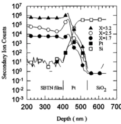
Figure 2 displays the bismuth SIMS depth profiles of the SBTN films with x51.7, 2.5, and 3.2. The Bi diffusion through the Pt layer was also observed in this figure. A Bi concentration reaching maximum in the interface of SBTN and Pt bottom electrode implies the formation of Bi2Pt in the
interface. The Bi diffusion was also observed for the SBT films prepared by the sol-gel,1metal-organic decomposition
TABLE I. Chemical composition of 600 °C deposited SBTN films prepared by various radio-frequency power ratios.
Power ratio between Bi2O3 and Sr0.8Bi2.2Ta1.2Nb0.8O91y
targets
Mole ratio in SBTN film
Sr Bi Ta Nb 20/120W 0.860.05 1.760.05 1.260.05 0.960.05 20/110W 0.860.05 2.060.05 1.260.05 0.960.05 20/100W 0.860.05 2.560.05 1.260.05 0.960.05 20/90W 0.860.05 2.760.05 1.260.05 0.960.05 20/80W 0.860.05 2.960.05 1.260.05 0.960.05 20/70W 0.860.05 3.260.05 1.260.05 0.960.05
FIG. 1. XRD patterns of 600 °C deposited SBTN films prepared by various radio frequency power ratios.
FIG. 2. SIMS bismuth depth profiles of 600 °C deposited Sr0.8BixTa1.2Nb0.9O91y~x51.7, 2.5, and 3.2! films.
1096 J. Appl. Phys., Vol. 85, No. 2, 15 January 1999 Tsai, Lin, and Tseng
~MOD!,20,21 and metal-organic chemical vapor deposition
~MOCVD!22techniques. To elucidate the Bi
2Pt formed in the
interface, TEM examination was performed. The cross-sectional TEM image of x52.5 SBTN films @Fig. 3~a!# indi-cates that a layer of 12–40-nm-thick second phase forms at the interface of SBTN film and Pt bottom electrode and the SBTN film had columnar microstructure. The EDS analyses of SBTN, interface, and Pt bottom electrode were made with a 15-nm-diam probe and their spectra are shown in Fig. 3~b!. The signals of Cu and Si in Fig. 3~b! come from copper ring and Si substrate during TEM sample preparation using ion gun milling. The major elements at the interface are Bi and Pt. Therefore, the TEM-EDS analysis also reveals that the formation of BixPt second phase in the interface, most prob-ably is Bi2Pt. As generally recognized, it is extremely
diffi-cult for the Bi to get off the bismuth deficiency SBTN film and diffuse into the Pt layer at the deposition temperature of about 600 °C. Hence, according to Fig. 2, the Bi depth profile of x51.7 ~i.e., bismuth deficit! film is more uniform than that of x52.5 film. However, for films with x53.2 ~i.e., bismuth rich!, owing to the presence of Bi2O3 phase, evaporation of
Bi is expected to be more serious than diffusion. Therefore,
there is not significant bismuth depletion region in front of bismuth maximum peak ~Fig. 2!. The SIMS composition depth profiles of Sr0.8Bi2.5Ta1.2Nb0.9O91y films ~i.e., x52.5
film! indicate that Sr, Ta, and Nb were not diffused into the bottom electrode and their depth profiles are very uniform
~Fig. 4!. Similar behavior is also found in other films.
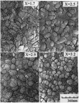
Figure 5 illustrates typical~FESEM! surface images ob-tained from SBTN films having various Bi contents. The films exhibit a somewhat porous structure with elongated grains. The grain size distribution of x51.7 film is nonuni-form. In addition, an increase of the bismuth content causes the grain size distribution to become more homogeneous. The average grain size of the x52.5, 2.9, and 3.2 films is about 96 nm. The root means square~rms! roughness of the film surfaces calculated from the AFM morphologies in a 5 mm35 mm area ~Fig. 6! reveals that the roughness of the films increases with an increase of the bismuth content. As generally assumed, increasing Bi content lowers the melting
FIG. 3.~a! The cross-sectional TEM image of Sr0.8Bi2.5Ta1.2Nb0.9O91yfilm deposited on Pt/SiO2/Si substrate.~b! EDS spectra acquired from the SBTN, interface, and Pt bottom electrode.
FIG. 4. SIMS depth profiles of Sr0.8Bi2.5Ta1.2Nb0.9O91y film deposited at
600 °C.
FIG. 5. FESEM surface images of Sr0.8BixTa1.2Nb0.9O91y~x51.7, 2.5, 2.9,
and 3.2! films.
point of the films, making it relatively easy to merge small grains into large rough grains during 600 °C deposition.
Figure 7 illustrates the remanent polarization~2Pr! and the coercive field ~2Ec! of the different bismuth content SBTN films at an electric field of 35 kV/cm. The SBTN films of x52.5 has a higher remanent polarization than the others, while the coercive fields~2Ec! of the films, except for x53.2, are close to 30 kV/cm. Figure 8 illustrates typical polarization versus electric field curves of Sr0.8Bi2.5Ta1.2Nb0.9O91y film recorded with23 to 13 V ex-citations. The 2Pr and 2Ec of Sr0.8Bi2.5Ta1.2Nb0.9O91y films were 52 mC/cm2 and 28 kV/cm at an electric field of 35
kV/cm, respectively. These excellent properties may be at-tributed to the unique solid solution of SrBi2Ta2O9 and SrBi2Nb2O9and the crystal orientation control, hence, the Pr
value of our SBTN films can be compared with that of PZT. Herein, the fatigue test of the Sr0.8Bi2.5Ta1.2Nb0.9O91y films
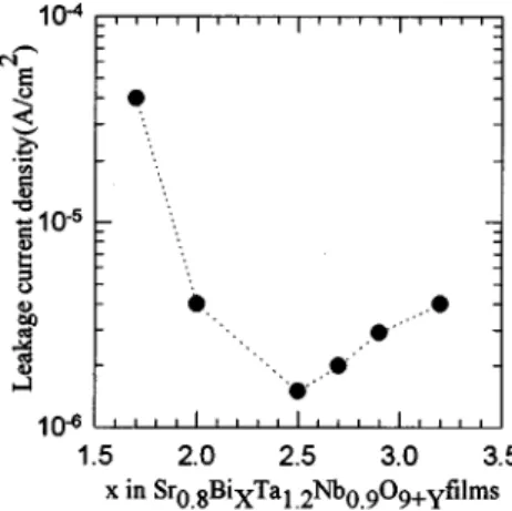
was performed using a bipolar square wave of 3 V at 1 MHz, which indicated that no fatigue was observed after the sample was switched up to 1.031010cycles. Figure 9 depicts the leakage current densities of the different bismuth content SBTN films at an electric field of 50 kV/cm. The current densities were measured after fabricating the Pt top elec-trodes followed by annealing in an atmosphere of O2 at
500 °C for 1 h. According to this figure, the Sr0.8Bi2.5Ta1.2Nb0.9O91y film exhibits minimum leakage
cur-rent density of about 1.531026 A/cm2at an electric field of 50 kV/cm and the Bi deficient films have larger leakage cur-rent than the Bi excess films. The leakage curcur-rent of our
films is higher than that of SBT films. The columnar crystal-lites, the possible Bi2Pt phase at the interface of SBTN/Pt
and the deviation from stoichiometry might be responsible for the higher leakage current density of the SBTN films.
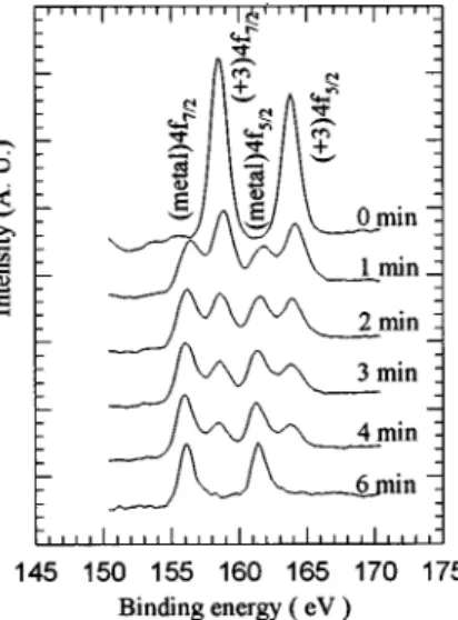
Figure 10 displays the dependence of the Bi signals from XPS of Sr0.8Bi2.5Ta1.2Nb0.9O91y film on the etching time.
The etching rate of the films was 25 nm/min. Obviously, the signal from the film surface is different from that inside. The intensity of the Bi13signal was high at the film surface and decreased with the etching time, while the intensity of the metallic Bi signal increased with depth. The binding energies of Bi134 f7/2 and 4 f5/2 core level photoemissions were lo-cated at 158.8 and 164.2 eV, respectively. The binding energy locations of the metallic bismuth 4 f7/2 and 4 f5/2 core levels, were at 156.4 and 161.8 eV, respectively. After 6 min etching, the amount of metallic Bi was extremely large and there was nearly no trace of Bi13. These phenom-ena were attributed to the cleavage of the O–Bi bonds during the Ar ions etching which made bismuth oxide de-composed and reduced to the metallic state.6,23 Figure 11 illustrates the dependence of the Nb signal from XPS of Sr0.8Bi2.5Ta1.2Nb0.9O91y film on the etching time. The
bind-ing energies of Nb153d5/2and 3d3/2are 206.6 and 209.4 eV,
respectively. After 6 min etching, a signal appeared from metallic Nb, and after 12 min etching, there was no further reduction of Nb15to Nb. Some of the Bi ions substitute for strontium in its site in Sr0.8Bi2.5Ta1.2Nb0.9O91y film. XPS
FIG. 6. Root mean square roughness of the various bismuth content SBTN films.
FIG. 7. The remanent polarization and coercive field of the various bismuth content SBTN films at 35 kV/cm electric field.
FIG. 8. P–E hysteresis loops of the Sr0.8Bi2.5Ta1.2Nb0.9O91yfilms.
FIG. 9. The current density of the various bismuth content SBTN films at 50 kV/cm electric field.
1098 J. Appl. Phys., Vol. 85, No. 2, 15 January 1999 Tsai, Lin, and Tseng
studies indicate that there was no lower valence state of bis-muth in the film surface except Bi13. Moreover, metallic Bi in the interior of the film was reduced from Bi13 during argon ion etching. Next, the film after 6 min etching was annealed at 500 °C in O2for 1 h and then, the XPS spectrum
of this film was recorded at the same spot as before. The metallic Bi and Nb in the interior were observed to be reoxi-dized to Bi13and Nb15states, which are the same as those on the surface of the film. Hence, there was still no lower valence state of bismuth in strontium site. Table II lists the binding energies of this annealed film.
IV. CONCLUSIONS
The bismuth layer structured Sr0.8BixTa1.2Nb0.9O91ythin
films with x51.7, 2.0, 2.5, 2.7, 2.9, and 3.2 were grown on Pt/SiO2/Si substrates at low temperature of 600 °C by
two-target off-axis radio-frequency magnetron sputtering. These films exhibited~115! as the dominant plane and showed
co-lumnar morphology. When x>2.9, Bi2O3second phase was
found in the film. These films had a low coercive field~2Ec! of about 30 kV/cm at an applied field of 35 kV/cm. In addi-tion, the Sr0.8Bi2.5Ta1.2Nb0.9O91y film had a larger remanent
polarization~2Pr! of 52mC/cm at 35 kV/cm than other com-position films, and also demonstrated fatigue free character-istics up to 1.031010switching cycles under a 3 V bipolar 1
MHz square wave. Moreover, XPS depth profiles studies of Sr0.8Bi2.5Ta1.2Nb0.9O91y film indicated not only that Bi13 and Nb15 appear in both the surface and interior of as-deposited films, but also that bismuth substituted in the strontium site of x52.5 films still remains in its 13 valence state.
ACKNOWLEDGMENT
The author would like to thank the National Science Council of the Republic of China for financially supporting this research under Contract No. NSC 87-2112-M009-037.
1
T. Y. Tseng, Proceedings of 1996 International Electron Devices and Ma-terials, C2-5, Tsing-Hua University, Hsinchu, Taiwan, 1996, p. 89. 2T. Mihara, H. Yoshimori, H. Watanabe, and C. A. Araujo, Jpn. J. Appl.
Phys., Part 1 34, 5233~1995!. 3
T. J. Boyle, C. D. Buchheit, M. A. Rodriguez, H. N. Al-Shareef, B. A. Hernandez, B. Scott, and J. W. Ziller, J. Mater. Res. 11, 2274~1996!. 4K. Amanuma, T. Hase, and Y. Miyasaka, Appl. Phys. Lett. 66, 221
~1995!.
5P. Y. Chu, R. E. Jones, Jr., P. Zurcher, D. J. Taylor, B. Jiang, S. J. Gillespie, Y. T. Lii, M. Kottke, P. Fejes, and W. Chen, J. Mater. Res. 11, 1065~1996!.
6S. Ono, A. Sakakibara, T. Seki, T. Osaka, I. Koiwa, J. Mita, and T. Iwabuchi, J. Electrochem. Soc. 144, L185~1997!.
7
R. Dat, J. K. Lee, O. Auciello, and A. I. Kingon, Appl. Phys. Lett. 67, 572 ~1995!.
8H. M. Yang, J. S. Luo, and W. T. Lin, J. Mater. Res. 12, 1145~1997!. 9T. Osaka, A. Sakakibara, T. Seki, S. Ono, I. Koiwa, and A. Hashimoto,
Jpn. J. Appl. Phys., Part 1 37, 597~1998!. 10
H. Watanabe, T. Mihara, H. Yoshimori, and C. A. Paz de Araujo, Jpn. J. Appl. Phys., Part 1 34, 5240~1995!.
11T. Atsuki, N. Soyama, T. Yonezawa, and K. Ogi, Jpn. J. Appl. Phys., Part 1 34, 5096~1995!.
12M. A. Rodriguez, T. J. Boyle, B. A. Hernandez, C. D. Buchheit, and M. O. Eatough, J. Mater. Res. 11, 2282~1996!.
13T. Matsuki, Y. Hayashi, and T. Kunio, Tech. Dig. Int. Electron Devices Meet., 691~1996!.
14N. Ichinose and M. Watanabe, Jpn. J. Appl. Phys., Part 1 36, 5893~1997!. 15
S. S. Park, C. H. Yang, S. G. Yoon, J. H. Ahn, and H. G. Kim, J. Elec-trochem. Soc. 144, 2855~1997!.
16H. M. Tsai, P. Lin, and T. Y. Tseng, Appl. Phys. Lett. 72, 1787~1998!. 17I. Koiwa, T. Kanehara, J. Mita, T. Iwabuchi, T. Osaka, and S. Ono, Jpn. J.
Appl. Phys., Part 1 36, 1597~1997!. 18
S. B. Desu, D. P. Vijay, X. Zhang, and B. P. He, Appl. Phys. Lett. 69, 1719~1996!.
19S. B. Desu and D. P. Vijay, Mater. Sci. Eng., B 32, 75~1995!. TABLE II. Binding energy of 600 °C deposited Sr0.8Bi2.5Ta1.2Nb0.9O91y film.
Energy level Valence state Binding energy~eV!
Bi 4 f7/2 4 f5/2 13 158.860.2 164.260.2
Nb 3d5/2 3d3/2 15 206.660.2 209.460.2
Ta 4 f7/2 4 f5/2 15 25.560.1 27.360.1
Sr 3d5/2 3d3/2 12 133.160.2 135.660.1
O 1s 22 529.660.2
FIG. 10. Etching time dependence of bismuth XPS signals of Sr0.8Bi2.5Ta1.2Nb0.9O91yfilm.
FIG. 11. Etching time dependence of niobium XPS signals of Sr0.8Bi2.5Ta1.2Nb0.9O91yfilm.
20T. Hayashi, H. Takahashi, and T. Hara, Jpn. J. Appl. Phys., Part 1 35, 4952~1996!.
21T. Noguchi, T. Hase, and Y. Miyasaka, Jpn. J. Appl. Phys., Part 1 35, 4900~1996!.
22N. J. Seong, C. H. Yang, W. C. Shin, and S. G. Yoon, Appl. Phys. Lett.
72, 1374~1998!.
23Y. Oishi, Y. Matsumuro, and M. Okuyama, Jpn. J. Appl. Phys., Part 1 36, 5896~1997!.
1100 J. Appl. Phys., Vol. 85, No. 2, 15 January 1999 Tsai, Lin, and Tseng