Highly Stable SrZrO3 Bipolar Resistive Switching Memory by Ti Modulation Layer
Ming-Chi Wu1, Meng-Han Lin1, Yu-Ting Yeh1, Chen-Hsi Lin2, and Tseung-Yuen Tseng1
1 Department of Electronics Engineering and Institute of Electronics
National Chiao Tung University, Hsinchu 300, Taiwan
2 Winbond Electronics Corporation, Hsinchu 300, Taiwan
In this study, we investigated the resistive switching characteristics of the SrZrO3 (SZO)-based resistance random access memory
(RRAM). After the sequential thin-films Pt/Ti/SZO/LaNiO3
deposition, the post annealing (PA) treatment under various conditions was carried out to form the interfacial layer (TiOx)
between Ti and SZO. It can be proved that the Ti modulation layer act as an oxygen getter can modify the resistive switching property of RRAM. With the suitable thickness of Ti layer and the proper annealing temperature, the SZO-based RRAM device could have a lower operation voltage, a lower compliance current a long retention behavior, and stable resistance ratio over 104 s under 0.3 V reading voltage.
Introduction
The researchers have extensively studied several next-generation nonvolatile memories due to the physical limitation. Among the studied memories, the resistive random access memory (RRAM) have attracted the most interest due to its advantages of high speed operation, low power consumption, excellent retention, and simple structure to realize ultrahigh density integration. Several metal oxides with resistive switching behavior have been used in RRAM device, such as TiO2 (1), NiO (2), ZrO2 (3), and
Al2O3 (4), as well as perovskite oxides including SrZrO3(SZO) (5), (Pr, Ca)MnO3
(PCMO) (6), and Bi4Ti3O12 (7). However, several key issues on the RRAM, including
instability of operation parameters, low switching endurance, and poor yield, need to be overcome before using to replace the conventional nonvolatile memories. In this paper, we demonstrate the SZO-based RRAM in Pt/Ti/SZO/LaNiO3 (LNO) structure with
bipolar switching behavior, in which the Ti metal layer acts as an oxygen getter to modify the resistive switching property. Therefore, the SZO-based RRAM with good endurance, stable operation parameters, and high yield could be appropriate for next generation nonvolatile memory application.
Experimental Procedure
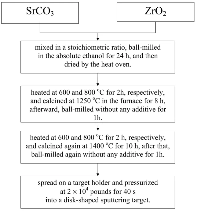
Preparation of the SZO and LNO targets
The fabrication of the SZO target use as the sputtering source to deposit SZO thin films was shown as the following. First, the SrCO3 and ZrO3 powders were mixed in a
stoichiometric ratio, and then their mixed power was ball-milled in the absolute ethanol for 24 h to ensure a homogeneous mixing and particle size reduction. After the mixture was dried by the heat oven, the dried powder was separately heated at 600 oC and 800 oC
ball-mill the calcined powder for 1h, separately heat it at 600 oC and 800 oC for 2 h, and calcined it at 1400 oC for 10 h to improve crystallinity. The second calcined powder was also ball-milled again without any additive for 1 h to obtain the final SZO power. Finally, the SZO powder was spread on a target holder and pressurized at 2 × 10⁴ pounds for 40 s
to form a disk-shaped sputtering target. The fabrication flow of SZO sputtering target is listed in Fig. 1.
Figure 1. The fabrication flow chart of the SZO sputtering target.
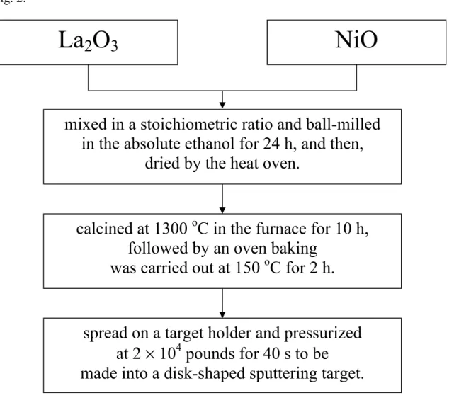
The LNO sputtering target was prepared in the following method, similar to SZO fabrication process. At first, the La2O3 and NiO powder were mixed in a stoichiometric
ratio and ball-milled in the absolute ethanol for 24 h. The dried powder was calcined at 1300 oC for 10 h, and then baked at 150 oC for 2 h. Eventually, the LNO powder was also spread on a target holder and pressurized at 2 × 10⁴ pounds for 40 s into a disk-shaped
SrCO
3
ZrO
2
mixed in a stoichiometric ratio, ball-milled
in the absolute ethanol for 24 h, and then
dried by the heat oven.
heated at 600 and 800
oC for 2h, respectively,
and calcined at 1250
oC in the furnace for 8 h,
afterward, ball-milled without any additive for
1h.
heated at 600 and 800
oC for 2 h, respectively,
and calcined again at 1400
oC for 10 h, after that,
ball-milled again without any additive for 1h.
spread on a target holder and pressurized
at 2
× 10
4pounds for 40 s
sputtering target. The fabrication flow chart of LNO sputtering target is summarized in Fig. 2.
Figure 2. The fabrication flow chart of the LNO sputtering target. Fabrication of SZO-based RRAM device
The 200-nm thick wet oxide was grown on 4-inch Si wafer as the starting substrate for the RRAM devices. After the 80-nm Pt/ 20-nm Ti layer was deposited on oxide substrate by electron beam evaporation, the 120-nm LNO conducting films were deposited on by radio-frequency (RF ) sputtering system at 250 oC in a Ar + O2 mixed
gas ambient (Ar/O2 = 3: 2). The sputtering power and the working pressure were set to
150 W and 10 mTorr, respectively. And then, the rapid thermal annealing (RTA) process was carried out at 600 oC in O2 ambient for 60 s to enhance the crystallinity of the LNO
film with highly (100) and (200)-orientations [5]. A 20-nm resistive switching layer, a SZO film, was deposited on the LNO/Pt/Ti/SiO2 substrates by RF sputter at 500 oC under
10 mTorr in Ar/O2 mixed gas ambient. The inserted Ti layers with the thicknesses of 40
nm and 100 nm were deposited onto SZO thin film, and then the 80-nm thick Pt capping layer with a diameter of 150 μm was deposited by shadow mask to form Pt/Ti/SZO/LNO/Pt/Ti/oxide structure. After depositing all stack films, the post annealing (PA) treatment was carried out to form the interfacial layer (TiOx) between Ti and SZO
thin film at temperatures ranging from 200 oC to 300 oC for 1 h.
La
2
O
3
NiO
mixed in a stoichiometric ratio and ball-milled
in the absolute ethanol for 24 h, and then,
dried by the heat oven.
calcined at 1300
oC in the furnace for 10 h,
followed by an oven baking
was carried out at 150
oC for 2 h.
spread on a target holder and pressurized
at 2
× 10
4pounds for 40 s to be
Results and Discussion
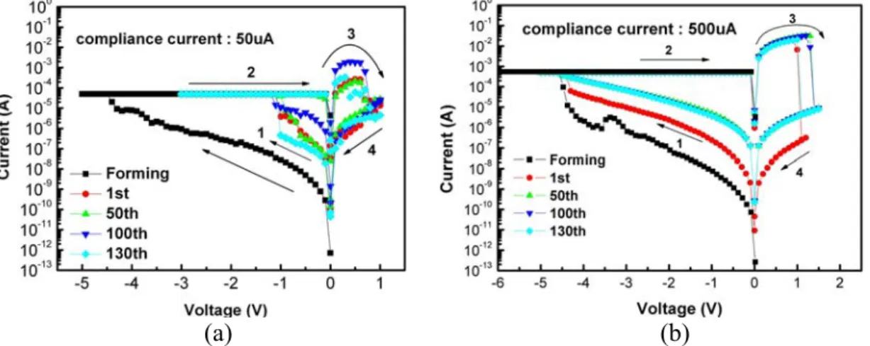
The SZO film of the RRAM device in the original state must be subjected to a forming process before operating as a resistive switching device. Fig. 3(a) shows the IV curves of the SZO-based RRAM device with 40-nm-thick Ti layer subjected to 200 oC PA process (denoted as: Ti40-200). Its forming voltage is approximate -3.5 V to -4.5 V with a compliance current of 50 μA. It is noteworthy that the compliance current protects the RRAM device form hard breakdown. After the forming process, the device switches to high current state (H-state) due to formation the conducting filament, and then, the voltage sweep reached to a positive approximately 1 V, the device switches to low current state (L-state) attributed to rupture the filament, which is defined as turn-off process. Further applying negative voltage, the device switches from L-state back to H-state, which is defined as turn-on process. The reproducibility of up to 130 cycles promises stable and uniform switching characteristics. The arrows in the figure denote the voltage sweeping direction. Fig. 3(b) depicts the IV curve of a SZO film with 40-nm-thick Ti layer and as deposited (denoted as: Ti40-as). The Ti40-200 device shows lower turn-on voltage and compliance current than Ti40-as.
(a) (b)
Figure 3. Typical I-V curves of the SZO-based RRAM device with 40-nm Ti layer subjected to 200 oC PA process, and (b) without PA process.
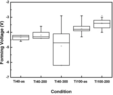
To clarify the influence of Ti layer and PA process on the resistive switching behaviors, the IV characteristics of the other control samples, including of Ti40-300, Ti100-as, and Ti100-200 are also measured. The forming voltages and operation voltages of various SZO memory devices are demonstrated in Figs. 4 and Fig. 5 pointing out that Ti40-200 device has more stable forming voltage and lowest turn on voltage.
Figure 4.Statistical chart for various forming voltages of SZO-based RRAM devices
Figure 5. Statistical chart for various operation voltages of SZO-based RRAM devices.
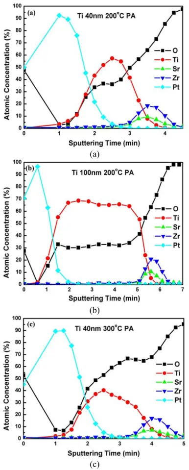
Fig. 6(a), 6(b), and 6(c) show the X-ray Photoelectron Spectrometer (XPS) depth profiles of oxygen, titanium, strontium, zirconium, and platinum elements in Ti40-200, Ti100-200, and Ti40-300 devices, respectively. It indicates that oxygen content in the Ti layer increases as the increase of the thickness of Ti layer and annealing temperature, which causes oxygen vacancies in the SZO thin film.
(a)
(b)
(c)
Figure 6. XPS depth profiles of various SZO-based RRAM devices under (a) Ti40-200, (b) Ti100-Ti40-200, and (c) Ti40-300 conditions, respectively.
According to the bipolar switching behavior of Pt/Ti/SZO structure devices and oxygen depth profiles, we can conclude a possible mechanism. A reaction between Ti and SZO thin films makes a thin TiOx film and leads to SZO thin film having a number
of oxygen vacancies during post annealing. During the forming process, the generation of other defects, i.e., oxygen vacancies in the SZO thin film due to high electric field, which align to form the conducting paths. Meanwhile, the oxygen ions migrate from the TiOx
layer to the SZO thin film and the TiOx-y are formed by reduction process, resulting in the
L-state switch to H-state. When a positive bias is applied, the oxygen ion are attracted from the SZO to the TiOx-y thin film and the TiOx-y layer is further oxidized to TiOx by
the assistance of local joule heating leading to the H-state switch to L-state. Under the negative bias, the oxygen ions migrate from the TiOx layer to the SZO thin film so that
the oxidation state of the TiOx is reduced again. As the above mention, the TiOx layer,
which serves as an oxygen sink, captures and releases the oxygen ions during the switching of the applied voltage. So, the conduction filaments could be formed and ruptured at the interface through the reduction and oxidation of the TiOx layer,
respectively. The possible switching mechanism is shown in Fig. 7.
Figure 7. A demonstration of the possible switching mechanism.
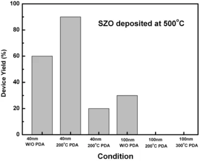
Fig. 8 displays the yield probability of the SZO thin film device with various conditions. The Ti40-200 device shows the best yield. The better SZO resistive switching memory device can be made with the appropriate oxygen vacancies in the SZO film and the proper TiOx film formed by suitable annealing temperature and thickness of Ti layer.
Pt (-V) TiOx SZO LNO (ground) TiOx O O Pt (-V) TiOx SZO Oxygen defect LNO (ground) Pt (+V) TiOx SZO LNO (ground) O2 O2 TiOx-y Turn off Turn on Formi ng Pt TiOx SZO LNO TiOx-y Pt TiOx SZO LNO TiOx O O Turn on Turn off
Figure 8. The yield probability of the SZO based RRAM device with various conditions.
For memory application, the retention test of Ti40-200 device is carried out at room temperature and 85 oC, which was measured under 0.3 V. The resistance ratio of between L-state and H-state which range covers around four orders of magnitude and both memory states can be retained for more than 106 s without any external electrical power, as shown in Fig. 9.
Figure 9. Data retention characteristics of the Ti40-200 device for H-state and L-state measured under 0.3 V at room temperature and 85 oC.
Besides, the nondestructive readout test was also performed at room temperature and 85 oC under stress voltage of 0.3 V, both memory states are stable up to 104 s, which is presented in Fig. 10.
Figure 10. Nondestructive readout property of the Ti40-200 device at room temperature and 85 oC under stress voltage of 0.3 V
Conclusion
In summary, the bipolar resistance switching behavior of Pt/Ti/SZO/LNO RRAM devices with stable and reproducible characteristics was performed. The influences of Ti modulation layer and PA on the properties of the devices were investigated. The Ti40-200 device showing lower operation voltage, lower compliance current, long retention behavior, and stable resistance ratio over 104 s under 0.3 V stress. Such a device has good performances such as, good endurance, stable operation parameters, and high yield, which is appropriate for next generation nonvolatile memory application.
Acknowledgments
This work was supported by the Winbond Electronics Corporation, Taiwan, and by the National Science Council, Taiwan, under project NSC 96-2628-E-009-166.
References
1. M. Fujimoto, H. Koyama, Y. Hosoi, K. Ishihara, and S. Kobayashi, Jpn. J. Appl.
Phys., 45, L310 (2006)..
2. D. W. Kim, B.H. Park, R. Jung, and S. Seo, Jpn. J. Appl. Phys., 46, 5205 (2007). 3. C. Y. Lin, S. Y. Wang, D. Y. Lee, and T. Y. Tseng, J. Electrochem. Soc., 155,
H615 (2008)
4. C. Y. Lin, C. Y. Wu, C. Y. Wu, C. Hu, and T. Y. Tseng, J. Electrochem. Soc., 154, G189 (2007)..
5. C. C. Lin, C. C. Lin, B. C. Tu, J. S. Yu, C. H. Lin, and T. Y. Tseng, Jpn. J. Appl.
Phys., 46, 2153 (2007).