Highly Efficient and Stable Inverted Polymer Solar Cells
Integrated with a Cross-Linked Fullerene Material as an
Interlayer
Chao-Hsiang Hsieh, Yen-Ju Cheng,* Pei-Jung Li, Chiu-Hsiang Chen, Martin Dubosc, Ru-Meng Liang, and Chain-Shu Hsu*
Department of Applied Chemistry, National Chiao Tung UniVersity, 1001 Ta Hsueh Road Hsin-Chu, 30010 Taiwan
Received January 11, 2010; E-mail: [email protected]; [email protected]
Abstract: A novel PCBM-based n-type material, [6,6]-phenyl-C61-butyric styryl dendron ester (PCBSD), functionalized with a dendron containing two styryl groups as thermal cross-linkers, has been rationally designed and easily synthesized. In situ cross-linking of PCBSD was carried out by heating at a low temperature of 160°C for 30 min to generate a robust, adhesive, and solvent-resistant thin film. This cross-linked network enables a sequential active layer to be successfully deposited on top of this interlayer to overcome the problem of interfacial erosion and realize a multilayer inverted device by all-solution processing. An inverted solar cell device based on an ITO/ZnO/C-PCBSD/P3HT:PCBM/PEDOT:PSS/Ag configuration not only achieves enhanced device characteristics, with an impressive PCE of 4.4%, but also exhibits an exceptional device lifetime without encapsulation; it greatly outperforms a reference device (PCE ) 3.5%) based on an ITO/ZnO/P3HT:PCBM/PEDOT:PSS/Ag configuration without the interlayer. This C-PCBSD interlayer exerts multiple positive effects on both P3HT/C-PCBSD and PCBM/C-PCBSD localized heterojunctions at the interface of the active layer, including improved exciton dissociation efficiency, reduced charge recombination, decreased interface contact resistance, and induction of vertical phase separation to reduce the bulk resistance of the active layer as well as passivation of the local shunts at the ZnO interface. Moreover, this promising approach can be applied to another inverted solar cell, ITO/ZnO/C-PCBSD/PCPDTBT:PC71BM/PEDOT:PSS/Ag, using PCPDTBT as the p-type low-band-gap conjugated polymer to achieve an improved PCE of 3.4%. Incorporation of this cross-linked C60interlayer could become a standard procedure in the fabrication of highly efficient and stable multilayer inverted solar cells.
Introduction
Polymeric solar cells (PSCs) have emerged as a promising alternative technique for producing clean and renewable energy due to their potential for fabrication onto large areas of lightweight flexible substrates by low-cost solution processing. To maximize the donor-acceptor heterojunction interfacial area for efficient exciton dissociation, mainstream PSC devices adopt the concept of a bulk heterojunction (BHJ), where an active layer contains a p-type donor and an n-type acceptor to form an interpenetrating nanoscale network.1 A conventional BHJ PSC with an active layer sandwiched by a low-work-function aluminum cathode and a hole-conducting poly(3,4-ethylene-dioxylenethiophene):poly(styrenesulfonic acid) (PEDOT:PSS) layer on top of an indium tin oxide substrate is the most widely used and investigated device configuration. On the basis of this device architecture, high power-conversion efficiencies (PCEs)
of ca. 4-5% have been achieved using a blend consisting of a regioregular poly(3-hexylthiophene) (P3HT) and a fullerene derivative, [6,6]-phenyl-C61-butyric acid methyl ester (PCBM).2
Along with high performance, long-term stability is a growing concern for PSCs. However, it is highly challenging to develop a PSC that can achieve a high PCE while maintaining good ambient stability of the device. Prolonged exposure to air rapidly reduces the performance of unencapsulated conventional de-vices. Many mechanisms are proposed to explain the decay. First, oxygen and moisture can diffuse to the active layer through grain boundaries and pinholes in the metal electrode, which in turn degrades the organic active materials. Second, due to direct contact, the aluminum electrode can easily penetrate the active layer, leading to chemical reactions and alteration of the intrinsic properties of semiconductors. As a result, metal oxides such as a titanium oxide or zinc oxide buffer layer have been inserted between the organic active layer and the Al electrode to improve (1) (a) Yu, G.; Gao, J.; Hummelen, J. C.; Wudl, F.; Heeger, A. J. Science
1995, 270, 1789. (b) Halls, J. J. M.; Walsh, C. A.; Greenham, N. C.; Marseglia, E. A.; Friend, R. H.; Moratti, S. C.; Holmes, A. B. Nature 1995, 376, 498. (c) Thompson, B. C.; Fre´chet, J. M. J. Angew. Chem., Int. Ed. 2008, 47, 58. (d) Gu¨nes, S.; Neugebauer, H.; Sariciftci, N. S. Chem. ReV. 2007, 107, 1324. (e) Brabec, C. J.; Sariciftci, N. S.; Hummelen, J. C. AdV. Funct. Mater. 2001, 11, 15. (f) Coakley, K. M.; MeGehee, M. D. Chem. Mater. 2004, 16, 4533. (g) Cheng, Y.-J.; Yang, S.-H.; Hsu, C.-S. Chem. ReV. 2009, 109, 5868.
(2) (a) Woo, C. H.; Thompson, B. C.; Kim, B. J.; Toney, M. F.; Fre´chet, J. M. J. J. Am. Chem. Soc. 2008, 130, 16324. (b) Reyes-Reyes, M.; Kim, K.; Carroll, D. L. Appl. Phys. Lett. 2005, 87, 083506. (c) Li, G.; Yao, Y.; Yang, H.; Shorotriya, V.; Yang, G.; Yang, Y. AdV. Funct. Mater. 2007, 17, 1636. (d) Li, G.; Shrotriya, V.; Huang, J.; Yao, Y.; Moriarty, T.; Emery, K.; Yang, Y. Nat. Mater. 2005, 4, 864. (e) Mayer, A. C.; Scully, S. R.; Hardin, B. E.; Rowell, M. W.; McGehee, M. D. Mater. Today 2007, 10, 28. (f) Ma, W.; Yang, C.; Gong, X.; Lee, K.; Heeger, A. J. AdV. Funct. Mater. 2005, 15, 1617.
Recently reported inverted devices based on P3HT/PCBM composite exhibited PCEs in the range of ca. 2-4%, which is inferior to that of regular solar cells, presumably due to poor electrical coherence at the organic/inorganic interfaces.5f-h,6 Self-organization of a fluorinated PCBM buffer layer on top of a P3HT/PCBM active layer has been shown to improve the photovoltaic performance of a regular PSC.7It is believed that
incorporating an additional n-type C60 derivative interlayer
between the inorganic metal oxide and the organic active layer in an inverted solar cell might improve device performance by modulating the electronic and orbital interactions at the upper and bottom interfaces.
The major obstacle to realizing such a multilayer inverted device by cost-effective solution processing is that the deposited C60 derivative interlayer must possess sufficient resistance
against the organic solvent used in processing the sequential active layer to prevent interfacial erosion.8 A C
60 derivative
having a carboxylic acid group that forms a self-assembled monolayer (SAM) on the metal oxide surface has been suc-cessfully used to enhance the device characteristics.5c,9 The
potential drawbacks for SAM formation are incomplete coverage at the molecular scale and probable desorption of this monolayer during wet processing, creating localized defects in this inter-layer.10Very recently, a cross-linkable polythiophene has been
successfully used to improve the thermal stability of a PCS by
chemically fixing the optimized morphology of the active layer.11Moreover, this cross-linking approach also allows for fabricating a bilayer solar cell device by solution processing.11
As a result, development of a fullerene material that can be solution-deposited on a substrate and readily undergo chemical cross-linking to form a robust and immobilized layer could be a straightforward and ideal strategy. With this distinct interlayer, mutual diffusion between the upper active layer and the bottom metal oxide layer, leading to direct contact, can be avoided. Styrene is known to be a superb thermally curable group because it can undergo rapid polymerization in the solid state to form polystyrene without the use of any initiators.12Therefore, we have designed and synthesized a fullerene derivative, [6,6]-phenyl-C61-butyric styryl dendron ester (PCBSD), that contains
a small dendron functionalized with two thermally cross-linkable styryl groups. Herein, we report a generally applicable and effective approach that integrates an interlayer of this cross-linked PCBSD (C-PCBSD) into inverted solar cells, achieving not only superior device performance but also remarkable long-term stability.
Results and Discussion
In the presence of 1-ethyl-3-(3-(dimethylamino)propyl)car-bodiimide (EDC) and 4-(dimethylamino)pyridine (DMAP), PCBSD was easily prepared by esterification of styrene-containing dendron SD with [6,6]-phenyl-C61-butyric acid
(PCBA), which was obtained by the hydrolysis of PCBM (Scheme 1).13The core structure of PCBSD is based on the
most widely used n-type material, PCBM; therefore, PCBSD is expected to inherit all the excellent electrical properties of its parent, PCBM.
The thermal transition properties of PCBSD monomer were investigated by the first scan of differential scanning calorimetry (DSC). It showed a broad exothermic peak with a Tmaxvalue
around 149 °C, which clearly indicates thermal cross-linking of styrene groups (Figure S1, Supporting Information). In (3) (a) Lee, K.; Kim, J. Y.; Park, S. H.; Kim, S. H.; Cho, S.; Heeger,
A. J. AdV. Mater. 2007, 19, 2445. (b) Gilot, J.; Barbu, I.; Wienk, M. M.; Janssen, R. A. J. Appl. Phys, Lett. 2007, 91, 113520. (c) Yang, C.; Kim, J. Y.; Cho, S.; Lee, J. K.; Heeger, A. J.; Wudl, F. J. Am. Chem. Soc. 2008, 130, 6444. (d) Yip, H.-L.; Hau, S. K.; Baek, N. S.; Ma, H.; Jen, A. K.-Y. AdV. Mater. 2008, 20, 2376. (e) Kim, J. Y.; Kim, S. H.; Lee, H.-H.; Lee, K.; Ma, W.; Gong, X.; Heeger, A. J. AdV. Mater. 2006, 18, 572.
(4) Sahin, Y.; Alem, S.; de Bettignies, R.; Nunzi, J.-M. Thin Solid Films 2005, 476, 340.
(5) (a) Li, G.; Chu, C.-W.; Shrotriya, V.; Huang, J.; Yang, Y. Appl. Phys. Lett. 2006, 88, 253503. (b) Hau, S. K.; Yip, H.-L.; Baek, N. S.; Zou, J.; O’Malley, K.; Jen, A. K.-Y. Appl. Phys. Lett. 2008, 92, 253301. (c) Hau, S. K.; Yip, H.-L.; Acton, O.; Baek, N. S.; Ma, H.; Jen, A. K.-Y. J. Mater. Chem. 2008, 18, 5113. (d) Liao, H.-H.; Chen, L.-M.; Xu, Z.; Li, G.; Yang, Y. Appl. Phys. Lett. 2008, 92, 173303. (e) Waldauf, C.; Morana, M.; Denk, P.; Schilinsky, P.; Coakley, K.; Choulis, S. A.; Brabec, C. J. Appl. Phys. Lett. 2006, 89, 233517. (f) Mor, G. K.; Shankar, K.; Paulose, M.; Varghese, O. K.; Grimes, C. A. Appl. Phys. Lett. 2007, 91, 152111. (g) White, M. S.; Olson, D. C.; Shaheen, S. E.; Kopidakis, N.; Ginley, D. S. Appl. Phys. Lett. 2006, 89, 143517. (h) Yu, B.-Y.; Tsai, A.; Tsai, S.-P.; Wong, K.-T.; Yang, Y.; Chu, C.-W.; Shyue, J.-J. Nanotechnology 2008, 19, 255202. (6) Steim, R.; Choulis, S. A.; Schilinsky, P.; Brabec, C. J. Appl. Phys.
Lett. 2008, 92, 093303.
(7) Wei, Q.; Nishizawa, T.; Tajima, K.; Hashimoto, K. AdV. Mater. 2008, 20, 2211.
(8) (a) Liang, C.-W.; Su, W.-F.; Wang, L. Appl. Phys. Lett. 2009, 95, 133303. (b) Huang, J.-S.; Chou, C.-Y.; Lin, C.-F. Sol. Energy Mater. Sol. Cells 2010, 94, 182.
(9) Hau, S. K.; Yip, H.-L.; Ma, H.; Jen, A. K.-Y. Appl. Phys. Lett. 2008, 93, 233304.
(10) Goh, C.; Scully, S. R.; McGehee, M. D. J. Appl. Phys. 2007, 101, 114503.
(11) Kim, B. J.; Miyamoto, Y.; Ma, B.; Fre´chet, J. M. J. AdV. Funct. Mater. 2009, 19, 2273.
(12) (a) Cheng, Y.-J.; Liu, M. S.; Zhang, Y.; Niu, Y.; Huang, F.; Ka, J.-W.; Yip, H.-L.; Tian, Y.; Jen, A. K.-Y. Chem. Mater. 2008, 20, 413. (b) Huang, F.; Cheng, Y.-J.; Zhang, Y.; Liu, M. S.; Jen, A. K.-Y. J. Mater. Chem. 2008, 18, 4495.
(13) Hummelen, J. C.; Knight, B. W.; LePeg, F.; Wudl, F. J. Org. Chem. 1995, 60, 532.
addition, the vibrational stretching of the vinyl groups at 1622 cm-1in the PCBSD completely disappears in the IR spectrum after the thermal treatment, again undoubtedly proving the occurrence of cross-linking (Figure 1a). These results reveal that the two arms of the dendron provide adequate flexibility for styryl groups to react in the solid state. After the initial heating cycle, a high Tgvalue of ca. 142°C was observed during the
second DSC heating, indicating that the resultant C-PCBSD is highly amorphous. Additionally, the cross-linked network prevents the diffusion of PCBSD molecules, which can reduce the tendency toward crystallization and maintain long-term morphological stability of the fullerene film (Figure S1).14In spite of its cross-linkable property, PCBSD can be stably stored at room temperature without the need for nitrogen protection. After the thermal cross-linking condition of PCBSD was determined, a multilayer inverted solar cell device A based on the configuration ITO/ZnO/C-PCBSD/P3HT:PCBM(1:1, w/w)/ PEDOT:PSS/Ag was fabricated. The electron-selective layer of ZnO nanoparticles was first prepared on ITO according to the literature.15A solution of PCBSD was spin-coated on top of
the ZnO surface, followed by thermal curing at 160°C for 30 min.
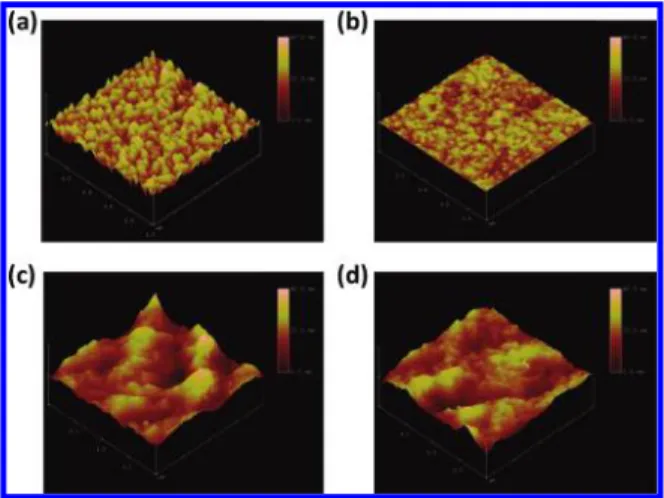
To prove that the cross-linked network of PCBSD is unambiguously generated on top of the ZnO, atomic force microscopy (AFM) and contact angle measurements were performed (Figure 2a,b). The bare ZnO/ITO surface exhibited a root-mean-square (rms) roughness of 3.16 nm and a wetting angle to DI water of 42°. After a layer of cross-linked PCBSD was deposited on top of the ZnO/ITO, the surface roughness decreased significantly to 0.6 nm, and the contact angle increased to 95° (Figure S2). These results reveal that voids in the uneven ZnO nanostructure surface are completely filled and covered by the PCBSD to form a smoother and more hydrophobic surface. By using an R-step profilometer, the thickness of the cross-linked layer is estimated to be approximately 10 nm, which indicates that the thin film consists of multiple layers of PCBSD molecules. Most importantly, this cross-linked network produced a robust and adhesive thin film with sufficient solvent resistance, evidenced by the almost unchanged absorption spectra measured before and after rinsing with dichlorobenzene (Figure 1b). Note
that the absorption intensity of the non-cross-linked layer is completely gone after rinsing with dichlorobenzene, indicating that without thermal curing, this thin layer can be totally washed out by the solvent used in the following spin coating.
The solvent resistance allows sequential active materials dissolved in dichlorobenzene to be successfully spin-coated on the C-PCBSD layer without destroying it. Unlike the case of a self-assembled monolayer C60modifier, which cannot planarize
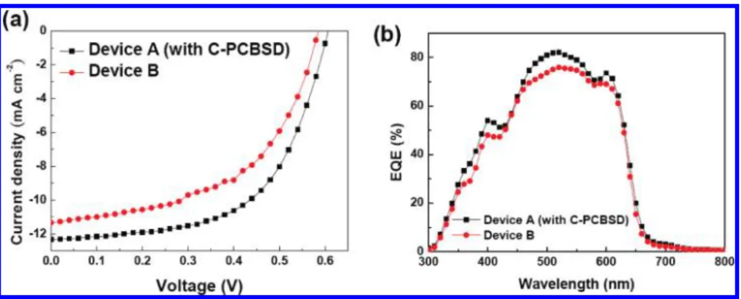
the metal oxide surface, the insertion of this C-PCBSD interlayer guarantees that the upper active layer and the bottom ZnO layer can be fully separated. Finally, a solution of PEDOT:PSS was then spin-cast, followed by vacuum deposition of silver as the anode. Under identical fabrication conditions, reference device B, using an ITO/ZnO/P3HT:PCBM(1:1, w/w)/PEDOT:PSS/Ag configuration (without the C-PCBSD interlayer), was prepared for comparison. The device characteristics and J-V curves of devices A and B are shown in Table 1 and Figure 3a. Under AM 1.5 G illumination at 100 mW/cm2, this standard device B
showed a PCE of 3.5%, which agrees well with the values reported in the literature based on P3HT/PCBM blend inverted solar cells.5b With an additional interlayer of C-PCBSD, the
PCE of device A was substantially improved to 4.4%. This value not only represents a 26% improvement over device B but also reaches a performance comparable to that of state-of-the-art regular solar cells based on the P3HT/PCBM system. The overall improved PCE of device A is the result of its (14) (a) Zhong, H.; Yang, X.; deWith, B.; Loos, J. Macromolecules 2006,
39, 218. (b) Drees, M.; Hoppe, H.; Winder, C.; Neugebauer, H.; Sariciftci, N. S.; Schwinger, W.; Scha¨ffler, F.; Topf, C.; Scharber, M. C.; Zhu, Z.; Gaudiana, R. J. Mater. Chem. 2005, 15, 5158. (15) (a) O’Brien, S.; Koh, L. H. K.; Crean, G. M. Thin Solid Films 2008,
516, 1391. (b) Musat, V.; Rego, A. M.; Monteiro, R.; Fortunato, E. Thin Solid Films 2008, 516, 1512.
Figure 1. (a) Infrared spectra of the PCBSD precursor and cross-linked PCBSD thin film. (b) Absorption spectra of the cross-linked PCBSD before (squares) and after (circles) rinsing with dichlorobenzene and non-cross-linked PCBSD layer after rinsing with dichlorobenzene (triangles).
Figure 2. AFM tapping mode height images of the surface of bare ZnO (a) and a C-PCBSD thin film on top of the ZnO (b) (1.0× 1.0 µm) and topography images of P3HT:PCBM films on top of the C-PCBSD interlayer (c) and on top of the ZnO layer (d) after thermal annealing at 140°C for 10 min (2.0× 2.0 µm).
simultaneously enhanced open-circuit voltage (Voc), short-circuit
current (Jsc), and fill factor (FF) relative to device B.
Because the BHJ active layer contains a p-type P3HT and an n-type PCBM component, both P3HT and PCBM domains at the interface are expected to make contact with the bottom layer to form two types of localized heterojunction at nanoscale size. Therefore, device A contains P3HT/C-PCBSD (denoted as LH-A1) and PCBM/C-PCBSD (LH-A2) localized hetero-junctions at the interface, whereas device B has P3HT/ZnO (LH-B1) and PCBM/ZnO (LH-B2) at the interface (Figure 4).
To carefully analyze the characteristic differences between devices A and B, we first consider only the microscopic heterojunctions LH-A1 and LH-B1, at which the P3HT domain in the active layer is exposed to the bottom layer in the interface. First, in device A, the C-PCBSD interlayer provides an extra P3HT/C-PCBSD interface area for ultrafast exciton dissociation, which is more efficient than the P3HT/ZnO interface in device B.16Second, the LUMO energy level of C-PCBSD (3.8 eV) is located between the LUMO of P3HT (3.3 eV) and the conduction band of ZnO (4.4 eV). Therefore, the C-PCBSD can function as an energy gradient intermediate, so that electrons can be efficiently transported to the ZnO through an energetically downhill cascade pathway.17These advantages might be
as-sociated with the improvement in Jscfrom 11.6 mA cm-2in
device B to 12.8 mA cm-2in device A. Third, considering that the energy offset between the conduction band of ZnO and the HOMO energy of P3HT (5.2 eV) is only 0.8 eV, charge recombination at the P3HT/ZnO interface in device B is thus very likely. With n-type C-PCBSD acting as a hole-blocking
buffer layer in device A, back electron transfer from ZnO to either the C-PCBSD interlayer or P3HT in the active layer can be greatly suppressed, which in turn helps enhance Vocand FF
in device A. Although charge recombination is also possible at the P3HT/C-PCBSD interface in device A, the much larger (16) (a) Beek, W. J. E.; Wienk, M. M.; Janssen, R. A. J. AdV. Funct. Mater.
2006, 16, 1112. (b) van Hal, P. A.; Christiaans, M. P. T.; Wienk, M. M.; Kroon, J. M.; Janssen, R. A. J. J. Phys. Chem. B 1999, 103, 4352.
(17) Niu, Y.-H.; Liu, M. S.; Ka, J. W.; Jen, A. K.-Y. Appl. Phys. Lett. 2006, 88, 093505.
Figure 3. (a) J-V curves of devices A and B under AM 1.5 G illumination at 100 mW/cm2. (b) IPCE spectra of devices A and B.
Figure 4. Schematic illustration of the multilayer inverted solar cell ITO/ ZnO/P3HT:PCBM(1:1, w/w)/PEDOT:PSS/Ag with (device A) and without (device B) a C-PCBSD interlayer. Device A contains two localized heterojunctions, LH-A1 and LH-A2, at the active layer interface, whereas device B has LH-B1 and LH-B2 at the interface. The architectures of devices A and B, with energy diagrams of the four localized heterojunctions at the interfaces, are shown.
energy offset of 1.4 eV at this interface, compared to 0.8 eV at P3HT/ZnO in device B, is still beneficial for reducing its probability.
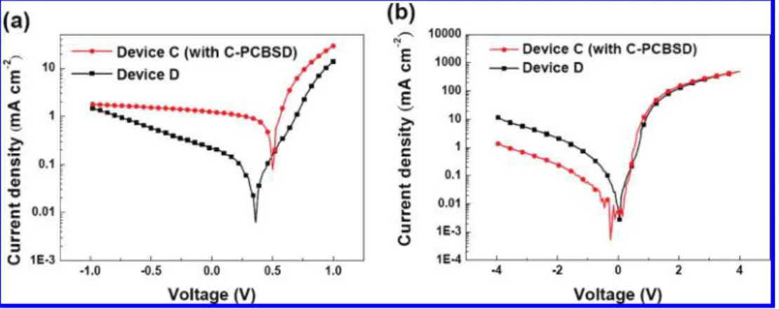
To prove the aforementioned multifunctionality of the C-PCBSD interlayer in device A, planar heterojunction device C (ITO/ZnO/C-PCBSD/P3HT/PEDOT:PSS/Ag) and device D (ITO/ZnO/P3HT/PEDOT:PSS/Ag) were fabricated and inves-tigated. Because such a simplified bilayer heterojunction completely eliminates the influence of PCBM in the active layer, so that the exciton dissociation and charge recombination sites are located mainly at the interface of the heterojunction, the macroscopic characteristics of devices C and D can reflect the microscopic properties of LH-A1 in device A (P3HT/C-PCBSD/ ZnO) and LH-B1 in device B (P3HT/ZnO), respectively.
Figure 5a shows the J-V characteristics of the planar heterojunction devices under AM 1.5 G illumination. As expected, device C showed dramatic improvement in all device characteristics relative to device D (Table. 1). The significantly increased Jsc value verifies that the exciton dissociation
ef-ficiency of the P3HT/C-PCBSD interface in device C is much higher than that of P3HT/ZnO in device D. Again, the charge recombination kinetics depends strongly on the energy offset at the n-type/p-type bilayer heterojunction. In comparison to device D with a Vocvalue of 0.36 V and an FF value of 32%,
an enlarged energy offset in device C reduces the carrier recombination rate and appreciably improves the Vocvalue to
0.5 V and the FF value to 50%. The J-V characteristics of devices C and D in the dark were also investigated (Figure 5b). Device C, with a C-PCBSD interlayer, showed a significant reduction in dark current under reverse bias, leading to a diode rectification ratio (current density at 3 V divided by current density at -3 V) higher by an order of magnitude than for device D (5.1× 10²vs 5.6 × 101). This result may suggest that the
C-PCBSD interlayer in device C can indeed passivate the local shunts at the ZnO interface and therefore block the injection of holes in the leakage pathways of the ZnO. This is also supported by the much increased shunt (parallel) resistance (Rsh) of devices
A (553 Ω cm2) and C (2913 Ω cm2) compared to their reference
devices B (292 Ω cm2) and D (1309 Ω cm2), respectively (Table
1). Consequently, the reduced leakage current leads to improved
Vocand FF values in device C.
After examining LH-A1 in device A and LH-B1 in device B, we further consider the microscopic properties of another localized heterojunction, PCBM/C-PCBSD (LH-A2) in device A and PCBM/ZnO (LH-B2) in device B (Figure 4). The electrochemical properties of the PCBSD were studied by cyclic voltammetry (Figure S3 and Table S1). It is not surprising to
observe that the chemically modified PCBSD has a LUMO energy level very similar to that of its parent PCBM (3.8 eV), thus forming ohmic contact with PCBM in the active layer of device A. In comparison to ZnO, which acts as an inorganic electron-selective layer in device B, the C-PCBSD interlayer in device A serves as an organic electron-selective layer. The obvious advantage of device A over device B is that the ohmic contact and organic-organic interface can enhance electrical coupling and lower the contact resistance, facilitating electron transport through the interface. As a result, electrons in the PCBM domain can be effectively extracted by the C-PCBSD interlayer from the active layer, where recombination is apt to take place due to directionless charge transport. Even though the bulk resistance as a result of the additional C-PCBSD layer may increase the series resistance (Rs), the overall series
resistance of device A (5.9 Ω cm2) is still smaller than that of
device B (6.2 Ω cm2), implying that the C-PCBSD interlayer
is indeed capable of reducing the contact resistance in device A.
To investigate the effect of the C-PCBSD interlayer on the morphology of the sequential active layer, AFM images under the tapping mode were used to trace differences in the surface topography of the P3HT:PCBM overlayer on ZnO and on C-PCBSD. After thermal annealing at 140°C for 10 min, the P3HT:PCBM layer on C-PCBSD showed a higher surface roughness of 4.61 nm (Figure 2c) compared to that on the ZnO surface with a roughness of 3.06 nm (Figure 2d). Due to the excellent compatibility and strong affinity between PCBM and C-PCBSD as well as the lower surface energy of P3HT, the active layer deposited on C-PCBSD tends to adopt a vertical phase separation in which the bottom side is PCBM-rich and the upper side is P3HT-rich. Therefore, the higher ordering of the P3HT domain close to the top surface leads to greater surface roughness. In addition, a comparison of the incident photon to current efficiency (IPCE) spectra (Figure 3b) shows that device A exhibits a more pronounced vibronic shoulder around 610 nm, indicating a higher degree of P3HT crystallinity, than device B. This type of distribution of n-type and p-type materials in the active layer is ideal for inducing directional charge carrier transportation in inverted solar cells.18
(18) (a) Campoy-Quiles, M.; Ferenczi, T.; Agostinelli, T.; Etchegoin, P. G.; Kim, Y.; Anthopoulos, T. D.; Stavrinou, P. N.; Bradley, D. D. C. Nat. Mater. 2008, 7, 158. (b) Xu, Z.; Chen, L.-M.; Yang, G.; Huang, C.-H.; Hou, J.; Wu, Y.; Li, G.; Hsu, C.-S.; Yang, Y. AdV. Funct. Mater. 2009, 19, 1227. (c) Kumar, A.; Li, G.; Hong, Z.; Yang, Y. Nanotechnology 2009, 20, 165202.
Figure 5. Semilogarithmic plots of J-V characteristics of heterojunction solar cell devices C and D (a) under AM 1.5 G illumination at 100 mW/cm2and
(b) in the dark.
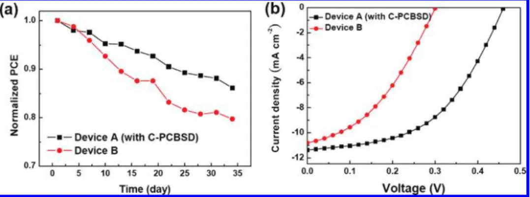
The PCEs of the unencapsulated inverted solar cell devices A and B were periodically measured for 35 days to monitor their long-term stability (Figure 6a). Device B retains 80% of the magnitude of its original PCE value after being exposed to ambient conditions for 35 days. In sharp contrast, the device performance of a regular solar cell (ITO/PEDOT:PSS/PCBM: P3HT/Ca/Al) without encapsulation decays very rapidly in just 2 days. This explicitly demonstrates the superior air stability of inverted solar cells. Most encouragingly, device A exhibited even better long-term stability than device B. The device degradation rate was quantified by plotting normalized PCEs as a function of time; the slopes were 4.1 × 10⁻³day-1 for device A and 6.6× 10⁻³day-1for device B (using the least-squares method). This result indicates that the C-PCBSD interlayer plays a key role in increasing the lifetime of device A by 1.5 times relative to that of device B.
Note that for most practical applications, a number of single cells must be connected in series to form a module producing sufficient voltage. Under illumination, if a single cell in the module is shaded and cannot absorb light, it is forced to be under reverse bias driven by the other illuminated cells to generate electrical power. Therefore, it is also crucial to evaluate the stability of a single cell under the influence of reverse bias. For this reason, we applied a voltage pulse of -5 V to devices A and B at a frequency of 2 Hz for 5 h under ambient conditions and then remeasured the J-V characteristics under AM 1.5 G at 100 mW/cm2(Figure 6b). The PCE of device B dropped
significantly to 1.2%, corresponding to a 66% loss of its original value prior to reverse bias stressing, whereas device A exhibited better stability against reverse bias, showing a 40% decay to obtain a much higher PCE of 2.6%. Device degradation is known to be related to leakage current caused by the formation of hot spots in bulk or at the interface.19The coverage of a
three-dimensional C-PCBSD network on ZnO might passivate the hot spots generated in the ZnO to suppress the leakage current, thus improving the operational lifetime. Additionally, without this interlayer as a dense and robust spacer, gradual mutual penetration between the ZnO and the active layer in device B may alter their chemical or physical properties as the operational time increases.
While recent research on inverted solar cells has concentrated mainly on device engineering on the basis of the typical P3HT/ PCBM system, the use of other low band gap p-type polymers has not been well explored due to their relatively low device performance. After successfully demonstrating that a C-PCBSD
interlayer can effectively improve the performance of a P3HT/ PCBM-based inverted solar cell, we envision that this strategy can be a general approach for extension and application to other blending systems using a low-band-gap polymer with better light-harvesting ability. A well-studied p-type polymer, poly[2,6-(4,4-bis(2-ethylhexyl)-4H-cyclopenta[2,1-b;3,4-b
′]dithiophene)-alt-4,7-(2,1,3-benzothiadiazole)] (PCPDTBT), with a band gap
of 1.4 eV, was chosen to test this idea.20Device E (ITO/ZnO/ C-PCBSD/PCPDTBT:PC71BM (1:2, w/w)/PEDOT:PSS/Ag) and
its corresponding reference device F without the C-PCBSD interlayer (ITO/ZnO/PCPDTBT:PC71BM (1:2, w/w)/PEDOT:
PSS/Ag) were therefore fabricated. Encouragingly, device E exhibited a Vocvalue of 0.66 V, a Jscvalue of 14.52 mA cm-2,
and an FF value of 35.4%, leading to a PCE value of 3.4%, which is a considerable improvement of 78% compared to device F (PCE ) 1.9%) without this C-PCBSD interlayer (Table 1 and Figure 7). The PCE of 3.4% again achieves a level comparable to that of a regular solar cell based on the PCPDTBT:PC71BM system.18To the best of our knowledge,
this is the first example of an inverted solar cell using a low-band-gap polymer other than P3HT that can obtain a PCE greater than 3%.
Conclusion
In conclusion, a novel PCBM-based n-type material, PCBSD, functionalized with a dendron containing two styryl groups as the thermal cross-linkers, has been rationally
(19) Steim, R.; Choulis, S. A.; Schilinsky, P.; Lemmer, U.; Brabec, C. J. Appl. Phys. Lett. 2009, 94, 043304.
(20) (a) Zhu, Z.; Waller, D.; Gaudiana, R.; Morana, M; Mu¨hlbacher, D.; Scharber, M.; Brabec, C. J. Macromolecules 2007, 40, 1981. (b) Chen, C.-H.; Hsieh, C.-H.; Dubosc, M.; Cheng, Y.-J.; Hsu, C.-S. Macro-molecules 2010, 43, 697.
Figure 6. (a) Normalized PCEs as a function of time for devices A and B stored for 35 days in air under ambient conditions. (b) J-V curves of devices A and B under AM 1.5 G illumination at 100 mW/cm2after -5 V reverse bias stressing at a frequency of 2 Hz for 5 h.
Figure 7. J-V curves of devices E and F under AM 1.5 G illumination at 100 mW/cm2.
designed and easily synthesized. In situ cross-linking of PCBSD was carried out by heating at a low temperature of 160°C for 30 min to achieve a robust and solvent-resistant network, enabling the fabrication of a multilayer inverted device by solution processing. This C-PCBSD interlayer has multiple positive effects on both n-type semiconductor/C-PCBSD and p-type semiconductor/C-semiconductor/C-PCBSD localized het-erojunctions at the interface of the active layer as well as the interface of ZnO. An inverted solar cell device based on the ITO/ZnO/C-PCBSD/P3HT:PCBM/PEDOT:PSS/Ag con-figuration not only demonstrates enhanced device character-istics, with an impressive PCE of 4.4%, but also possesses exceptional device lifetime without encapsulation, overcom-ing the stability-performance trade-off. Moreover, this promising approach can be applied to another inverted solar cell system using PCPDTBT/PC71BM as the active layer to
achieve an improved PCE of 3.4%. We envision that incorporation of the cross-linked C60interlayer could become
a standard procedure in the fabrication of highly efficient and stable multilayer inverted solar cells.
Acknowledgment. This work is supported by the National Science Council and “Aim for the Top University Plan” of the National Chiao Tung University and Ministry of Education, Taiwan. Supporting Information Available:Text, figures, and a table giving synthetic procedures, device fabrication details, DSC, contact angle, and cyclic voltammetry measurements, and1H
and13C NMR spectra. This material is available free of charge
via the Internet at http://pubs.acs.org. JA100236B