Thermal Leakage Improvement by Using a
High-Work-Function Ni Electrode in High-
TiHfO Metal–Insulator–Metal
Capacitors
K. C. Chiang,a,zC. C. Huang,aH. C. Pan,bC. N. Hsiao,bJ. W. Lin,aI. J. Hsieh,a C. H. Cheng,cC. P. Chou,cA. Chin,a H. L. Hwang,dand S. P. McAlistere a
Department of Electronics Engineering, Nano Science Technology Center, National Chiao-Tung University, University System of Taiwan, Hsinchu, Taiwan
b
Instrument Technology Research Center, National Applied Research Laboratories, Hsinchu, Taiwan
c
Department of Mechanical Engineering, National Chiao-Tung University, Hsinchu, Taiwan
d
Department of Electrical Engineering, National Tsing Hua University, Hsinchu, Taiwan
e
National Research Council of Canada, Ottawa, Canada
An unavoidable drawback when using high- dielectrics in capacitors is the small bandgap and the related reduction in the band-offset, which results in a large leakage current at elevated temperatures. We report improvements in the thermal leakage current by using Ni as a high-work-function top electrode for high- TiHfO capacitors. This avoids sacrificing the overall value by using a multilayer or laminate structure and results in better voltage linearity, which is important for analog/radio frequency integrated circuits.
© 2007 The Electrochemical Society. 关DOI: 10.1149/1.2422874兴 All rights reserved.
Manuscript submitted August 17, 2006; revised manuscript received October 19, 2006. Available electronically January 5, 2007.
Metal–insulator–metal 共MIM兲 capacitor development aims to achieve high-capacitance density devices using a simple integration process to yield multiple functions for system-on-chip共SOC兲 appli-cations. The technological trend has been to increase the value in the dielectrics, from using Al2O3 and then HfO2–Al2O31 and
Nb2O52to TiTaO3-5 or TiHfO6 共 ⬇ 45–50兲. However, one draw-back for higher MIM devices is that the smaller bandgaps 共EG兲 result in a large leakage current at elevated temperatures, so that the stored charge leaks from the capacitor 共Q = CV兲. This is also a challenge in flash memory7 and is unavoidable during integrated circuit共IC兲 operation, where there is a large device density in the circuit and high dc power dissipation. A possible solution is to add a high EGdielectric to form a multilayer8,9or laminate structure,1but the overall value and voltage coefficient of capacitance 共VCC兲 are then degraded. In this paper we report the use of a high-work-function共m兲 metal to reduce the leakage current, without sacrific-ing the capacitance density. By ussacrific-ing highmNi共5.1 eV兲 for high- TiHfO capacitors, the leakage current at 125°C was reduced by nearly 2 orders of magnitude compared with control devices which used an Al electrode共m= 4.1 eV兲. Economically it is also better to use Ni rather than Ir, which has been used previously in comple-mentary metal oxide semiconductors共CMOSs兲.9
Experimental
The devices were fabricated by first depositing 2m SiO2on a
Si wafer and then forming the lower capacitor electrode using physi-cal vapor deposit 共PVD兲-deposited TaN/Ta bilayers. The Ta was used to reduce the series resistance and the TaN served as a barrier layer between the high- TiHfO and the Ta electrode. Then, the TixHf1−xO共x ⬇ 0.6兲 dielectric was deposited by PVD, followed by
a 400°C oxidation and an annealing step to reduce the leakage cur-rent. Finally, Ni or the control Al was deposited and patterned to form the top capacitor electrode. Devices of various sizes were made, and those measured were typically 20⫻ 20 m in area. The fabricated devices were characterized by capacitance–voltage共C–V兲 and current-density–voltage共J–V兲 measurements using an HP4155B semiconductor parameter analyzer and an HP4284A precision LCR meter.
Results and Discussion
Electrical C–V and J–V characteristics.— Figure 1a shows the
C–V characteristics at various frequencies for 关Ni or Al兴/ TiHfO/TaN MIM capacitors having⬃11 fF/m2capacitance den-sity. The Ni electrode devices show better frequency dispersion and voltage independence共small VCC兲 than those using Al. This indi-cates that the magnitude of the barrier height, m, of the upper
z
E-mail: [email protected]
Figure 1.共a兲 C–V characteristic of 关Ni or Al兴/TiHfO/TaN capacitors
mea-sured at various frequencies and 共b兲 J–V characteristics of 关Ni or Al兴/ TiHfO/TaN capacitors measured at 25 and 125 °C.
Journal of The Electrochemical Society, 154共3兲 G54-G57 共2007兲
0013-4651/2007/154共3兲/G54/4/$20.00 © The Electrochemical Society G54
) unless CC License in place (see abstract). ecsdl.org/site/terms_use
address. Redistribution subject to ECS terms of use (see 140.113.38.11
electrode is important in improving the device performance. In Fig. 1b the J–V characteristics of the TiHfO MIM capacitors, measured at 25 and 125°C, show that the advantage of the Ni electrode is preserved at the higher temperature, even though the leakage cur-rents are both increased exponentially.
⌬C/C and VCC␣.— Capacitor voltage linearity is an important factor for MIM capacitors in silicon radio frequency共rf兲 and mixed-signal IC applications. This voltage dependence can be obtained by fitting the measured C–V characteristics using a second-order poly-nomial expression of the form
⌬C共V兲 = C0共␣V2+V兲 关1兴
Here C0is the capacitance at 0 V, and␣ and  represent the qua-dratic and linear voltage coefficients of capacitance, respectively. Because the effect of the linear  term can be compensated by appropriate circuit design共by using a differential method10-13兲, the ␣ term is the main parameter for the voltage dependence. Figure 2a depicts the variation of⌬C共V兲/C as a function of voltage for the 关Ni or Al兴/TiHfO/TaN capacitors at different frequencies. The lines in the figure are fits to the data using the expression above. The Ni top electrode not only reduces the leakage current but also improves the frequency dispersion,⌬C/C, and ␣. This improvement of the volt-age dependence may arise from the higher barrier heightm be-tween the electrode and the dielectric, which leads to a lower carrier concentration.14,15In general, the dispersive behaviors, such as the voltage and frequency dependence, are believed to be related to the existence of bulk-dielectric traps near the dielectric/metal interface. Different traps induce charges with different time constants and strongly modulate the capacitor charges at certain frequencies. Therefore, when the applied frequency is high, VCC is low because
the induced charges are unable to follow the ac signal.2-6
In addition, the stability of the devices after a thermal treatment of 350°C for 1 h was good, as indicated from the J–V and⌬C/C–V characteristics shown in Fig. 2b. This suggests that the devices are suitable for the fabrication of MIM structures in back-end-of-the-line共BEOL兲 processes.
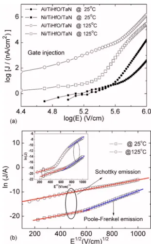
Current conduction mechanism.— To investigate the large leakage-current difference for the关Ni or Al兴/TiHfO/TaN MIM ca-pacitors, an understanding of the conduction mechanism is neces-sary. This is also useful in the development of advanced MIM de-vices. According to the space-charge-limited current 共SCLC兲 theory,16-18 the J–V characteristics should initially be ohmic 共J ⬃ V兲 at low applied bias. As the applied voltage is increased, a strong injection of the charge carriers into the bulk of the film oc-curs, giving J⬃ V2. Figure 3a shows the log共J兲 vs log共E兲
depen-dence. The slopes of the curves in both the low- and high-field regimes are not in agreement with the ohmic and SCLC mecha-nisms.
To investigate further, we have plotted ln共J兲 vs E1/2for Schottky
emission共SE兲 or Frenkel–Poole 共FP兲 conduction, as shown in Fig. 3b, i.e., J⬀ exp
冉
␥E 1/2− V b kT冊
关2兴 whereFigure 2. 共a兲 ⌬C/C–V characteristics of 关Ni or Al兴/TiHfO/TaN capacitors
and共b兲 J–V and ⌬C/C–V 共insert兲 for the Ni-based capacitors.
Figure 3.共Color online兲 共a兲 log共J兲 vs log共E兲 plots of 关Ni or Al兴/TiHfO/TaN
capacitors measured at 25 and 125°C共b兲 Measured and simulated J–E1/2of
an Al/TiHfO/TaN capacitor. A Ni/TiHfO/TaN device is shown in the inset. G55
Journal of The Electrochemical Society, 154共3兲 G54-G57 共2007兲 G55
) unless CC License in place (see abstract). ecsdl.org/site/terms_use
address. Redistribution subject to ECS terms of use (see 140.113.38.11
␥ =
冉
e3 0K⬁冊
1/2
关3兴 The constant is equal to 1 or 4 for the FP or SE cases. The fits to the experimental data give slopes ␥ of 1.65 or 3.32 ⫻ 10−5eV
共m/V兲1/2 for the SE or FP mechanisms, respectively, by using a
refractive index n = 2.45 for TixHf1−xO共x ⬇ 0.6兲.19This n value is consistent with a linear interpolation of the reported 2.57 value for
TiO2and 1.85 for HfO2.20The leakage current at 25°C for the Al
electrode on TiHfO/TaN is consistent with an SE description at low field and FP at high field through a trap-conduction mechanism. However, the leakage at 125°C appears to be dominated by the SE process, due to the small energy barrierb. In contrast, the leakage at 125°C for the Ni case is still governed by the SE and FP at low and high field, respectively, which is due to the largeb, as depicted in the figure insert.
Because the low-field conduction for both Ni and Al electrodes at 125°C is governed by SE, we have plotted the detailed ln共J/T2兲-E1/2relation in Fig. 4a to extract
b. A Schottky barrier height of 0.3 or 1.4 eV for Al/TiHfO or Ni/TiHfO was obtained, where the significantly largerbusing Ni accounts for the⬃2 or-ders of magnitude lower leakage current, compared with devices using Al. From the extractedband the reportedmdata, the con-duction band of the dielectric with respect to the vacuum level is at 3.8 eV; this gives an EG for TixHf1−xO of 4.3 eV with x⬇ 0.6. Because the conduction mechanism at high electric field for the Ni electrode on TiHfO is governed by an FP mechanism, we also plot-ted the ln共J/E兲-1/KT relationship in Fig. 4b. The extracted trap en-ergy is 1.2 eV from the conduction band of TiHfO, as shown in the inserted plot. This value is less than the SE energy of 1.4 eV, which supports the contention that the high-field conduction should be de-scribed as an FP process rather than an SE one. This result also explains that the conduction mechanism for the lowmAl electrode case should be governed by SE because its SE barrier height is only 0.3 eV, whereas the FP case requires 1.2 eV. Thus, the use of a high m electrode, such as Ni, is vital when using high- dielectrics which have small EGvalues.
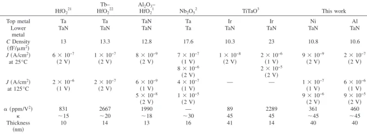
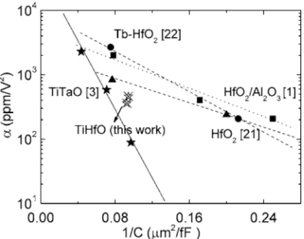
Performance comparison.— Table I summarizes the important device data for MIM capacitors with various high- dielectrics and work-function metals. The thermal leakage decreases with increas-ing m of the metal electrode from Al to Ni. High ⬃11 fF/m2 density, small quadratic VCC ␣ of 361 ppm/V2, and low 1
⫻ 10−7A/cm2leakage current at 125°C were simultaneously
mea-sured in the Ni/TiHfO/TaN devices, which is comparable with or better than other reported data. The VCC␣ is strongly dependent on the capacitance density and electric field;1-6,21-24an exponential de-crease of␣ with increasing capacitance effective thickness 共CET兲, or 1/C, was observed for all the capacitors, as shown in Fig. 5. The VCC␣ is also dependent on the specific high- dielectric, where Ta2O5exhibits superior VCC compared with HfO2and Al2O3.8In
addition, the metal-dielectric interface is also important for the VCC ␣ and formation of such an interfacial layer degrades the capaci-tance performance.23 Overall, MIM capacitors incorporating a
Figure 4. 共a兲 SE fitting of 关Ni or Al兴/TiHfO/TaN capacitor data at low
electric field and共b兲 FP fits of a Ni/TiHfO/TaN capacitor data at high field. The related band diagrams are included.
Table I. Comparison of device data for MIM capacitors with various high- dielectrics and work-function metals.
HfO221
Tb– HfO222
Al2O3–
HfO21 Nb2O52 TiTaO3 This work
Top metal Ta Ta TaN Ta Ir Ir Ni Al
Lower metal
TaN TaN TaN Ta TaN TaN TaN TaN
C Density 共fF/m2兲 13 13.3 12.8 17.6 10.3 23 10.8 10.6 J共A/cm2兲 at 25°C 6⫻ 10−7 共2 V兲 1⫻ 10 −7 共2 V兲 8⫻ 10 −9 共2 V兲 7⫻ 10 −7 共1 V兲 8⫻ 10−6 共2 V兲 1⫻ 10−8 共2 V兲 2⫻ 10 −6 共1 V兲 2⫻ 10−5 共2 V兲 9⫻ 10−9 共2 V兲 2⫻ 10 −7 共2 V兲 J共A/cm2兲 at 125°C 2⫻ 10−6 共1 V兲 2⫻ 10 −7 共2 V兲 6⫻ 10 −9 共1 V兲 5⫻ 10−8 共2 V兲 4⫻ 10−7 共1 V兲 1⫻ 10−5 共2 V兲 — — 1⫻ 10−7 共1 V兲 9⫻ 10−6 共2 V兲 6⫻ 10−6 共1 V兲 9⫻ 10−5 共2 V兲 ␣ 共ppm/V2兲 831 2667 1990 — 89 2289 361 460 ⬃15 ⬃20 ⬃18 ⬃30 45 45 ⬃45 ⬃45 Thickness 共nm兲 10 14 13 16 41 14 40 40
G56 Journal of The Electrochemical Society, 154共3兲 G54-G57 共2007兲
G56
) unless CC License in place (see abstract). ecsdl.org/site/terms_use
address. Redistribution subject to ECS terms of use (see 140.113.38.11
highermtop electrode and a higher dielectric provide a practical approach to achieve low thermal leakage and good VCC simulta-neously without reducing the capacitance density, as in a multilayer or laminate structure.
Conclusions
The thermal leakage current in MIM capacitors has been shown to be reduced by work-function tuning. High-performance TiHfO MIM capacitors were developed without sacrificing the overall value, which occurs when using a multilayer or laminate structure. This approach improved the voltage-dependent factor␣, which is important for analog/RF ICs.
Acknowledgment
This work has been partially supported by NSC 共95-2221-E-009-298兲 and TDPA DOIT MOEA 95-EC-17-A-01-S1-047 of Taiwan.
National Chiao Tung University assisted in meeting the publication costs of this article.
References
1. H. Hu, S. J. Ding, H. F. Lim, C. Zhu, M. F. Li, S. J. Kim, X. F. Yu, J. H. Chen, Y. F. Yong, B. J. Cho, D S. H. Chan, S. C. Rustagi, M. B. Yu, C. H. Tung, A. Du, D. My, P. D. Fu, A. Chin, and D. L. Kwong, Tech. Dig. - Int. Electron Devices Meet.,
2003, 379.
2. S. J. Kim, B. J. Cho, M. B. Yu, M.-F. Li, Y.-Z. Xiong, C. Zhu, A. Chin, and D. L. Kwong, VLSI Technical Digest, p. 56–57共2005兲.
3. K. C. Chiang, A. Chin, C. H. Lai, W. J. Chen, C. F. Cheng, B. F. Hung, and C. C. Liao, VLSI Technical Digest, p. 62–63共2005兲.
4. K. C. Chiang, C. C. Huang, A. Chin, W. J. Chen, S. P. McAlister, H. F. Chiu, J. R. Chen, and C. C. Chi, IEEE Electron Device Lett., 26, 504共2005兲.
5. K. C. Chiang, C. H. Lai, A. Chin, T. J. Wang, H. F. Chiu, J. R. Chen, S. P. McAlister, and C. C. Chi, IEEE Electron Device Lett., 26, 728共2005兲. 6. K. C. Chiang, C. C. Huang, A. Chin, W. J. Chen, H. L. Kao, M. Hong, and J. Kwo,
VLSI Technical Digest, p. 126–127共2006兲.
7. C. H. Lai, A. Chin, H. L. Kao, K. M. Chen, M. Hong, J. Kwo, and C. C. Chi, VLSI Technical Digest, p. 54–55共2006兲.
8. Y. K. Jeong, S. J. Won, D. K. Jwon, M. W. Song, W. H. Kim, O. H. Park, J. H. Jeong, H. S. Oh, H. K. Kang, and K. P. Suh, VLSI Technical Digest, p. 222–223 共2004兲.
9. C. H. Huang, D. S. Yu, A. Chin, W. J. Chen, C. X. Zhu, M.-F. Li, B. J. Cho, and D. L. Kwong, Tech. Dig. - Int. Electron Devices Meet., 2003, 319.
10. K.-S. Tan, S. Kiriake, M. de Wit, J. W. Fattaruso, C.-Y. Tsay, W. E. Mattthews, and R. K. Hester, IEEE J. Solid-State Circuits, 25, 1318共1990兲.
11. The International Technology Roadmap for Semiconductors, Semiconductor Indus-try Association, San Jose, CA共2003兲.
12. S. B. Chen, J. H. Lai, K. T. Chan, A. Chin, J. C. Hsieh, and J. Liu, IEEE Electron Device Lett., 23, 203共2002兲.
13. C. H. Huang, M. Y. Yang, A. Chin, C. X. Zhu, M. F. Li, and D. L. Kwong, IEEE MTT-S Int. Microwave Symp. Dig., 1, 507共2003兲.
14. S. Blonkowski, M. Regache, and A. Halimaou, J. Appl. Phys., 90, 1501共2001兲. 15. C. Zhu, H. Hu, X. Yu, S. J. Kim, A. Chin, M. F. Li, B. J. Cho, and D. L. Kwong,
Tech. Dig. - Int. Electron Devices Meet., 2003, 879.
16. M. A. Lampert and P. Mark, Current Injection in Solids, Academic Press, New York共1970兲.
17. K. Kao and W. Hwang, Electrical Transport in Solids, Pergamon Press, New York 共1981兲.
18. D. Lamp, Electrical Conduction Mechanisms in Thin Insulating Films, IEEE 共1967兲.
19. Q. Fang, J. Y. Zhang, Z. M. Wang, J. X. Wu, B. J. O’Sullivan, P. K. Hurley, T. L. Leedham, H. Davies, M. A. Audier, C. Jimenez, J. P. Senateur, and W. Boyd, Thin Solid Films, 428, 263共2003兲.
20. A. Palil, Handbook of Optical Constants, Academic Press, New York共1985兲. 21. X. Yu, C. Zhu, H. Hu, A. Chin, M. F. Li, B. J. Cho, D.-L. Kwong, P. D. Foo, and
M. B. Yu, IEEE Electron Device Lett., 24, 63共2003兲.
22. S. J. Kim, B. J. Cho, M.-F. Li, C. Zhu, A. Chin, and D. L. Kwong, VLSI Technical Digest, p. 77–78共2003兲.
23. K. C. Chiang, C. C. Huang, A. Chin, G. L. Chen, W. J. Chen, Y. H. Wu, and S. P. McAlister, IEEE Trans. Electron Devices, 53, 2312共2006兲.
24. S. J. Ding, H. Hu, C. Zhu, S. J. Kim, X. Yu, M. F. Li, B. J. Cho, S. H. Chan, M. B. Yu, S. C. Rustagi, A. Chin, and D. L. Kwong, IEEE Trans. Electron Devices, 51, 886共2004兲.
Figure 5. ⌬C/C-1/C plots. An exponential decrease of ␣ with increasing
dielectric thickness was observed.
G57
Journal of The Electrochemical Society, 154共3兲 G54-G57 共2007兲 G57
) unless CC License in place (see abstract). ecsdl.org/site/terms_use
address. Redistribution subject to ECS terms of use (see 140.113.38.11