A Wideband DVB Forked Shape Monopole Antenna
With Coupling Effect for USB Dongle Application
Cho-Kang Hsu and Shyh-Jong Chung, Senior Member, IEEE
Abstract—A novel wide-band printed antenna, named forked shape monopole antenna (FSMA), is proposed. The forked shape line structure is introduced to create a capacitive coupling effect to reduce the antenna size and enhance the impedance bandwidth. The proposed antenna is to be applied in a compact USB dongle. And it is designed for the reception of the digital video broad-casting (DVB) signal in the 470 860 MHz frequency band. In addition to the DVB application, the upper band limit of the FSMA even can be extended from 860 MHz to 1142 MHz, suitable for use in the Global System for Mobil Communication (GSM850/900). By employing the branched-line and forked shape configurations, an antenna with 86% impedance bandwidth(SWR 2 5) is provided. A prototype of the FSMA was constructed and demon-strated. Measured and simulated results for the FSMA alone and with real application on a laptop computer are obtained.
Index Terms—DTV, UHF antenna, USB dongle, wide band monopole antenna.
I. INTRODUCTION
N
OWADAYS, new digital video broadcasting (DVB) has been realized through UHF band and operated in many countries [1]. It can offer high quality video with greater multimedia and interactive capabilities. It may also provide large opportunities for business and replace all the conventional analog TV broadcasting in the near future. Recently, some promising DVB antennas for application in various devices have been reported, such as portable personal computers (PCs) [2], USB (Universal Series Bus) dongles [3], PMPs (Portable Media Players) [4], vehicles, and other DVB applications [5]–[9]. The DVB antennas studied in [2] are embedded within the narrow spacing between the display and the casing of a PC for operation as an internal antenna. This internal DVB antenna requires the presence of a large ground plane, such as the supporting metal frame of the display of the laptop computer, in order to achieve an operating bandwidth in the ultra high frequency (UHF) band. USB dongles are frequently used in laptop computers for providing additional functions such as the plug-and-play function for GSM wireless network access and DVB system application [3], etc. The dimensions of antennaManuscript received January 16, 2009; revised March 12, 2010; accepted March 22, 2010. Date of publication June 14, 2010; date of current version September 03, 2010. This work was supported in part by the National Science Council, R.O.C. under Contract NSC 97-2221-E-009-041-MY3.
The authors are with the Department of Communication Engineering, National Chiao Tung University, Hsinchu, Taiwan 30050, R.O.C. (e-mail: sjchung@cm.nctu.edu.tw)
Color versions of one or more of the figures in this paper are available online at http://ieeexplore.ieee.org.
Digital Object Identifier 10.1109/TAP.2010.2052545
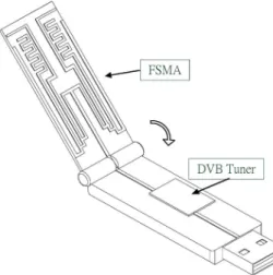
Fig. 1. Diagram of the FSMA in the USB dongle application.
and ground used in [3] are and
respectively, which are larger than normally used USB dongle size. PMP is also a popular hand-held device that combines DVB function. Some novel antennas have been demonstrated for used in PMPs [4], however, the designs were subject to a large ground plane (about ), or using protruded area from the housing of the PMP device. In the other hand, a conventional wire monopole antenna has a narrow impedance bandwidth. One of the techniques to improve the bandwidth required for the DVB system is to use a sleeve monopole antenna [5], [6], which suffers from a larger extra area for sleeve. The structure of the H-shape dipole antenna [7], fat dipole antenna with step-shaped feed gap [8], and folded dipole antenna with stubs [9] are also good to enhance bandwidth for DVB application. All the dimensions are over , which are more suitable for vehicle based than portable use.
In this paper, a forked shape monopole antenna (FSMA) is proposed to provide a small size and wide bandwidth applica-tion for DVB recepapplica-tion in the UHF band of 470 860 MHz. In addition to DVB application, the upper band limit of the pro-posed antenna even can be extended from 860 MHz to 1142 MHz that cover the GSM850/900 system. By employing the coupling branched-lines configuration, an antenna with 86% impedance bandwidth is provided. Fig. 1 illus-trates the diagram of the FSMA in a folded USB dongle, which possesses a small ground plane of size . The ground plane not only serves as the antenna ground but also the circuit ground for the DVB tuner. All the simulations in this study are performed by Ansoft HFSS (High Frequency Structure Simu-lator based on the finite element method) and AWR MWO (Mi-crowave Office). The former is used for full-wave
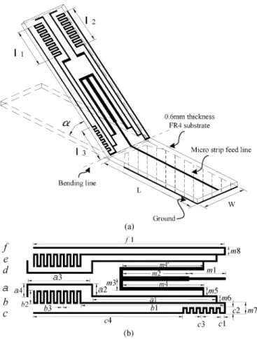
Fig. 2. (a) Geometry of the proposed FSMA for folded USB dongle applica-tion. (b) Detailed dimensions of the traces on the top substrate.
sional EM simulation, which is benefic to obtain the required antenna dimensions and performance. And the latter is for cir-cuit simulation, used for simulating the equivalent circir-cuit of the coupled strips structure.
II. ANTENNADESIGN
A. Antenna Concept
The proposed forked shape monopole antenna (FSMA) is a monopole-like planar antenna, with geometry and dimensions shown in Fig. 2. The antenna consists of two FR4 substrates with 0.6 mm thickness and . The top substrate of a size is printed with multi-forked shape metal strips, which functions as the main radiator of the antenna and also represents the foldable cover of the DVB USB dongle receiver. The bottom substrates with ground plane of dimensions
is reserved for the receiving circuitry. The two substrate are connected with a fold angle , as shown in Fig. 2(a). The antenna is excited by using a 50 microstrip line on the bottom substrate. As shown in Fig. 2(a), two bevels with angle of 45 are made on the ground plane for impedance matching. The widths of the metal strips are from 0.5 mm to 1.4 mm. The principal dimensions of the design are denoted in Fig. 2(b). Note that each element includes several sub-elements. For example, element- is composed of , , , and . The element- are defined at the left in Fig. 2(b).
The design for a specified FSMA is simple and clear. The forked line contains several pairs of symmetric metal traces and
TABLE I
TOTALLENGTHS ANDCORRESPONDINGRESONANTFREQUENCIES OFSEVERAL
ELEMENTSBELONGING TO THEFIRSRESONANCEGROUP
three inductive meandered lines designed to generate several resonant modes. These resonant modes can be divided into two groups that excited at different geometries. The first group of resonance has the characteristic that the excited current is dis-tributed mainly on a pair of traces in the whole forked line and is excited when the total path length from the feed point to the trace end equal to a quarter resonant wavelength. Referring to Fig. 2(b), the current fed to is divided into two equal parts entering strips and . Each strip is connected to three branches with different lengths, which provide different reso-nant paths for the incoming current. Due to the close spacing, mutual coupling occurs between any two adjacent traces, which results in a wide impedance bandwidth for the antenna (as will be demonstrated later). This group of resonance includes three resonant modes and generates a return loss bandwidth from 452 MHz to 800 MHz. For example, the total length of both wires and are about 165 mm that designed to generate a longest resonant path which corresponds to about a quarter wavelength at the lowest frequency of 460 MHz. The meander structures on the tops of the antenna and element-are designed to make this resonant path in small size. Besides, under the same total length of the meander portion, tuning the lengths of parts b2 and b3 can make optimum contribution of resonant modes to gain the better bandwidth and improve the impedance matching. The lengths of wires and correspond, respectively, to the resonant ones of the middle frequency 560 MHz and the highest frequency 750 MHz. Table I summarizes the total lengths and the corre-sponding resonant frequencies of several elements belonging to the first group type.
The second group of resonance generates a return loss band-width from 800 MHz to 1142 MHz. The meander portion in el-ement- is important for this resonance group since it functions as a current choke that helps to stop the high frequency current, leading to a shorter quarter-wavelength resonant path from the feed point to this meander portion. The main resonant mode of the second group is excited with current distributed on the outer paired traces, i.e., wire and . This path provides the resonant mode at about 980 MHz. The steps formed in wires
to help to excite the resonances of the second group. Be-sides, due to the bending structures in elements , these elements also provide other paths for extra resonances in the second group, which are contributive to extend the impedance bandwidth of the antenna.
The design steps for the proposed antenna can be listed as follows.
1) Design a monopole antenna of a quarter wavelength at the center frequency (650 MHz) of the DVB band (470 860 MHz);
Fig. 3. Simulated return loss of the proposed antenna with = 0 . The an-tenna dimensions are listed in Table II.
2) Add two branch strips to produce multiple resonances. The additional resonant frequencies are to be located at 460 MHz and 750 MHz;
3) Tuning the distance between strips to produce the coupling effect for combining the three resonant modes closely with continuous impedance bandwidth;
4) Create other resonant modes at higher frequency. To this end, add a meander structure that functions as a low pass filter at a suitable position to create an equivalent open cir-cuit for the high-frequency current. The meander struc-ture is placed at element- with the resonant path from feed line to the meander structure equal to a quarter wavelength of 980 MHz. Tune the meander structure to get an optimal current choke to support the multiple resonant modes on the second group.
Fig. 3 shows the simulated return loss of the proposed an-tenna with . It is seen that the bandwidth of
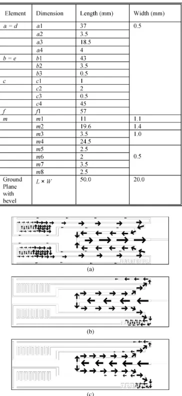
is 690 MHz, ranging from 452 MHz to 1142 MHz. The center frequencies of the first and second groups are located at 560 MHz and 980 MHz, respectively. To obtain this broadband antenna performance, the antenna parameters have been care-fully tuned with dimensions listed in Table II. In the optimiza-tion, it is found that suitably adjusting the distances between the metal traces would help to get a continuous return-loss band-width, instead of producing discrete resonance modes. This is because the impedance behavior at frequencies in between the resonant modes is sensitive to the coupling effect among the metal traces. Also, it is found that the best impedance bandwidth of the second group can be achieved when the current-choke me-ander portion is located in the outer pair of strips (element- or ). Fig. 4(a), (b), and (c) show, respectively, the current distri-butions at 460 MHz, 980 MHz, and 1100 MHz. It is seen that at the first frequency (in the first group), the current distributes over the strips and , and at the latter two frequencies (in the second group), the currents are blocked by the meander portion in element- .
The proposed FSMA provides multi-paths with proximity coupling to enhance bandwidth. The impedance bandwidths of the several excited resonant modes can not only cover the op-erating bandwidths of the DVB, but also can be extended to
TABLE II
PRINCIPALDIMENSIONS OF THEFSMA
Fig. 4. Typical current distributions of (a) the first group resonant mode at 460 MHz, (b) the second group mode at 980 MHz, and (c) the second group mode at 1100 MHz, = 0 .
GSM850 (824 MHz to 894 MHz)/900 (880 MHz to 960 MHz) system.
B. Coupling Effect of Closely Spaced Strips
To explain the mutual coupling effect occurred between any two adjacent traces of proposed antenna, let us consider the
Fig. 5. Configurations of (a) single strip and (b) dual strips monopole antennas. L = 50 mm, W = 20 mm, s1 = 75 mm, s2 = 67:5 mm, w1 = 1:4 mm, w2 = 1 mm, d = 3:4 mm, thickness of FR4 substrate = 0:75 mm.
Fig. 6. Simulated return losses of single strip and dual strips monopole antenna.
quarter-wavelength single-strip and dual-strips monopole an-tennas as shown in Fig. 5. The main strip of the dual-strips monopole has a length s1 of 75 mm, which is the same as the length of the single-strip monopole. And the second strip has a shorter length s2 of 67.5 mm and is parallel to the main one with a distance . Fig. 6 illustrates the simulation return losses of the single-strip antenna and the dual-strips one with distance equal to 3.4 mm and 0.8 mm. The optimal result of the single-strip monopole has a return-loss bandwidth of 528 MHz with the center frequency located at about 970 MHz. As the second strip is added with a distance of , as seen from the figure, a second resonant mode appears at a higher quency and pushes the original resonant mode to the lower fre-quency. When one reduces the distance d to 0.8 mm, stronger coupling between the two strips occurs and the two resonant modes merge into one. Notice that, as compared to that of the single-strip antenna, the new resonant mode of the dual-strips antenna with possesses a wider impedance band-width of 605 MHz and a lower resonant frequency (920 MHz). This demonstrates that, with suitable design, a close spaced par-allel strip would increase the impedance bandwidth and also re-duce the resonant frequency, or alternatively, rere-duce the required length, of the main strip.
To further expound the coupling effect of forked adjacent strips, a conceptual equivalent circuit of the dual-strips antenna
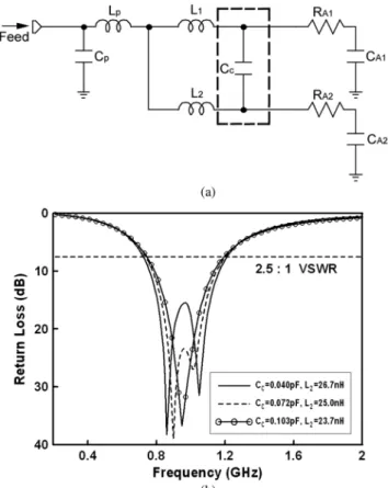
Fig. 7. (a) Corresponding equivalent circuit model of dual strips monopole an-tenna. (b) Simulated return losses for different values of coupled capacitance C . (C = 0:23 pF, L = 2:77 nH, L = 23:7 nH, R = 50:5 ohm, C = 1:36 pF, R = 53:4 ohm, C = 0:77 pF.)
in Fig. 5(b) is established as shown in Fig. 7(a), where the two radiating strips of about quarter-wavelength long are both mod-eled as a series RLC circuit with representing the radiation resistance [10]. The components and are used to con-sider the parasitic effect of the discontinuity structure where the microstrip feed line passes across the ground edge. A capaci-tance is placed in between the two RLC circuits to model the capacitive coupling between the two strips. To extract the components in this model, we first obtain the equivalent circuit of the first strip antenna alone and get the components of , , , , and . To this end, the parasitic components and are first gotten by full-wave simulating a structure formed by two back-to-back microstrip line discontinuities. The rest com-ponents in the equivalent circuit are then obtained by curve-fit-ting the calculated frequency response of return loss from the circuit model and the simulated response from HFSS. Secondly, the equivalent circuit with components of , , , , and for the second strip alone is established using the same pro-cedure as above. Note that the parasitic components and are identical to those for the first strip. Finally, we put the two equivalent circuits together, place a coupling capacitance be-tween them to get the final equivalent circuit [Fig. 7(a)], and then tune the value of until the equivalent circuit exhibits a sim-ilar frequency response as that of the dual strips monopole.
Fig. 7(b) presents the calculated return losses of the equiv-alent circuit for various coupling capacitance . When
Fig. 8. Simulated return loss for several values of .
equals 0.04 pF, two resonant modes are produced with fre-quency separation of 180 MHz. As increases, which means the two strips getting closer, the two resonant modes also get closer. The frequency separation reduces to 125 MHz when increases to 0.072 pF, which is exactly equal to that of in Fig. 6. Finally, when reaches 0.103 pF, the two modes merge into one. This modes degeneration behavior is just the same as that of the dual strips monopole. Note that in the above calculation, the value of deceases according to the increase of the coupling capacitance , since to reach a higher coupling capacitance, the distance d between strips should be shorter so that the total length of the second strip also becomes smaller. The reduction percentage of when increases from 0.072 pF to 0.103 pF is about 5.2%, which is close to the length reduction percentage of the second strip (from 3.4 67.5 to 0.8 67.5 mm, 3.7% reduction). Finally, it is noticed that although the coupling between strips is weak (i.e., small ), its effect on the antenna behavior is important and can not be ignored, especially when multiple closely-spaced strips, like the proposed antenna structure, are used.
In summary, by suitably controlling the spacing between the forked parallel strips, and thus the coupling capacitances, sev-eral grouped resonant modes can be generated, which is benefic to produce a wide impedance bandwidth and reduce the antenna size.
C. Antenna Parametric Study
To achieve a compact configuration for the USB dongle, the proposed antenna is designed as a folded type as shown in Fig. 2. Different fold angle may result in different antenna performance. Fig. 8 shows the influence of the fold angle on the return loss of the antenna. It is noticed that the increase of the angle deteriorates the impedance matching and thus decreases the bandwidth. Especially when the angle is over 90 , the impedance bandwidth reduces dramatically.
To see the effects of the FSMA structural parameters on the impedance bandwidth, several prototypes with various resonance lengths were constructed and studied by simulation. Fig. 9 shows the simulated return loss for various lengths
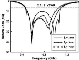
Fig. 9. Simulated return losses for several values of` : = 0 . Other param-eters are the same as indicated in Table II.
Fig. 10. Simulated return losses for several values of` . = 0 . Other pa-rameters are the same as indicated in Table II.
of the meander portion in element- (element- ) with . Other dimensions are the same as those given in Table II. The total strip lengths of the meander portion in element- for , 12.5, and 8.5 mm are, respectively, 59.5, 51.5, and 35.5 mm. From the obtained results it is seen that, the center frequency of the second group has little change, while that of the first group shifts to the higher frequency with the decrease of and . For , the obtained impedance bandwidth is the largest that can cover the lowest frequency of DVB system at 470 MHz. Fig. 10 shows the simulated return losses for various lengths of the meander portion in element- with , where is the length of the meander portion in element- [see Fig. 2(a)]. The total strip lengths of the meander portion in element- are 31, 21, and 16 mm, respectively, as , 9, and 7 mm. As stated earlier, the second group of resonance happens at the pair of wires and with dense current distributed in the meander portion. This can also be verified from Fig. 10 that changing the length of the meander portion in element- influences only the second group but not affects the first group. Note that the total impedance bandwidth is decreased with a decreased meander length . The reason is that decreasing the meander length
Fig. 11. Simulated input impedance on the Smith chart for various lengths of m2.
would deteriorate the function of the current choke, so that the incoming current may leak through the meander portion and diffuse into element- . This will make the resonance path of the second group longer, thus let the resonant modes move to the lower frequency.
Fig. 11 illustrates the variation of antenna impedance with the length of [see Fig. 2(b)]. The width of line is fixed as 1.4 mm. This line can be an impedance transformer that will make FSMA more suitable for different kinds of impedance system used. As shown, the real part of the impedance is increased when the length of increases. Since in this study the proposed FSMA is to be designed for use in a 50 system (like most of the devices), the length of would lead to the best return loss performance. The corresponding loop in the Smith chart is well centered and good impedance matching.
III. EXPERIMENTALRESULTS
A. Antenna Only
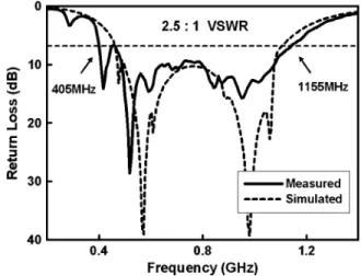
Based on the design dimensions shown in Table II, the proto-type of the proposed antenna was constructed and tested. Fig. 12 shows the measured return loss with the fold angle . The simulation result is shown here again for comparison. It is seen that the measurement roughly agrees with the simulation, with an impedance bandwidths of about 96% from 405 MHz to 1155 MHz. The cause of the experimental tolerance comes from the test cable that connects the antenna to the measurement equipment [11]. Note that in order to im-prove the measurement accuracy, a ferrite core (TDK, HF70) has been used in the test cable. From the measured data, several resonant modes in the first and second groups are successfully excited and the antenna shows a very wide impedance band-width that not only covers the required bandband-width of the DVB system from 470 MHz to 860 MHz, but also satisfies the band-width of the GSM850/900 system from 824 MHz to 960 MHz. In this study, the impedance bandwidth definition adopts 2.5:1 VSWR (about 7.3 dB return loss), which is a higher bandwidth standard for practical DVB and GSM applications. (Generally,
Fig. 12. Simulated and measured return loss of the proposed antenna with = 0 . The dimensions are the same as those in Table II.
Fig. 13. Measured total radiation field patterns of total power at 470, 700, 900, 1100 MHz with = 0 . (a) X-Y plane (b) Y-Z plane. (Unit: dBi)
the bandwidth definition is 5:1 VSWR or 3 dB return loss for DVB, and 3:1 VSWR or 6 dB return loss for GSM.)
The radiation characteristics of the proposed antenna were also studied. Fig. 13(a) and (b) plot the measured total radiation field patterns at 470, 700, 900, and 1100 MHz, respectively, for the fabricated prototype with in the and
planes. The radiation patterns are basically omnidirectional, with minor nulls in some directions. The measured peak gain varies from 0.9 dBi to 2.9 dBi in the frequency range.
B. Antenna With Notebook Computer
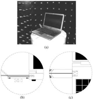
For a real application, the prototype of the folded FSMA was mounted at the side of a 14.1 notebook computer as shown in Fig. 14(a). The distance between the edge of the notebook and the bending line of the prototype antenna was set at 50 mm as
Fig. 14. (a) Photograph of the prototype antenna mounted in a notebook com-puter. (b) Side view and (c) top view of the antenna mounted in the notebook.
Fig. 15. Measured 3D total radiation field patterns with 14.1 notebook for various fold angles at (a) 500 MHz and (b) 900 MHz.
shown in Fig. 14(b). The ground plane of the prototype antenna was connected to the USB joint of the notebook that connected with the notebook ground plane as show in Fig. 14(c). Fig. 15 shows the three-dimensional measured radiation patterns of the mounted prototype antennas with different antenna fold angle at 500 MHz and 900 MHz. The display angle of the notebook was fixed at 110 as in the general use. Note that at the lower frequency (500 MHz), as observed from Fig. 15(a), the radia-tion patterns are almost the same as the fold angle is changed. This may be due to that at the lower frequency, quite a large part of the antenna current flows into the large ground plane of the notebook. This ground-plane current greatly contributes to the radiation field of the antenna, and thus dominantly deter-mines the total radiation pattern. On the other hand, when the frequency is shifted to 900 MHz, the antenna structure is larger
TABLE III
MEASUREDANTENNAGAIN ANDEFFICIENCY FOR THEPROPOSEDFSMAIN A
14.1 NOTEBOOK
Fig. 16. Measured peak gain versus frequency with different size of notebook.
as compared to the wavelength, thus less current is leaked to the ground plane and more current remains in the antenna area. This is why obvious changes of radiation patterns due to the variation of the fold angel can be observed in Fig. 15(b). Table III summa-rizes the measured results of the gain and efficiency. From the measurement, it is seen that the efficiency decreases with the in-crease of the fold angle . The best efficiency performances that appear with are 59.62% at 500 MHz and 62.51% at 900 MHz. The corresponding peak gain is about 2.35 dBi and 2.25 dBi, respectively.
The performance of the proposed antenna mounted in another notebook computer of 11.1 with a small size ground plane was also checked. As one knows, different sizes of the ground plane for applications will influence the return loss of a monopole-like antenna. This is also the case for the proposed antenna struc-ture, especially for the first resonant group. However, although not shown here, the measured return losses are still better than 7.3 dB (2.5:1 VSWR) over the full bandwidth for both the 11.1 and 14.1 notebooks. Fig. 16 illustrates the measured antenna peak gains at various frequencies for the popularly used dimen-sions of 11.1 and 14.1 notebooks. The antenna fold angle is fixed at 0 . The measured radiation gain of antenna only is also shown for comparison. The result shows that the performance of the antenna mounted in the notebooks is better than that of antenna only with a gain enhancement of about 3.5 dBi. This is because the antenna current is not crowded in the small an-tenna area and can be distributed to the large ground plane of the notebook, which helps to reduce the power loss in the antenna and thus increase the antenna efficiency and gain. Also notice from the figure that the antenna gain has little variance when the dimension of ground plane changed from 11.1 to 14.1 note-book. Ground size of 11.1 notebook is enough for the proposed FSMA.
IV. CONCLUSION
A novel wide-band DVB antenna has been proposed for the USB dongle reception. With the use of the multi forked-shaped structure, the impedance bandwidth of the proposed antenna oc-cupies all the used UHF bandwidth of the DVB system and can even cover the GSM850/900 system. Detailed design consider-ations for the antenna have been described. The performance of the proposed antenna mounted in notebook computers with different antenna angles and notebook sizes was also demon-strated. Good radiation characteristics were obtained. The pro-posed wideband DVB antenna, which has a compact antenna size of 60 by 20 with a ground plane of 50 by 20 and a folded structure, would be very attractive for USB dongle applications.
REFERENCES
[1] Digital Television Major Initiatives of Federal Communications Com-mission [Online]. Available: http://www.fcc.gov/dtv/
[2] C. M. Su, L. C. Chou, C. I. Lin, and K. L. Wong, “Internal DTV re-ceiving antenna for laptop application,” Microwave Opt. Technol. Lett., vol. 44, pp. 4–6, Jan. 2005.
[3] W. Y. Li, K. L. Wong, and S. W. Su, “Broadband integrated DTV an-tenna for USB dongle application,” Microwave Opt. Technol. Lett., vol. 49, pp. 1018–1021, May 2007.
[4] Y. S. Yu, S. G. Jeon, H. Park, D. H. Seo, and J. H. Choi, “Internal low-profile metal-plate monopole antenna for DTV portable multi-media player applications,” Microwave Opt. Technol. Lett., vol. 49, pp. 593–595, Mar. 2007.
[5] H. D. Chen, “Compact broadband microstrip-line-fed sleeve monopole antenna for DTV application and ground plane effect,” IEEE Antennas
Wireless Propag. Lett., vol. 7, 2008.
[6] K. G. Thomas, N. Lenin, and M. Sreenivasan, “Wide-band dual sleeve antenna,” IEEE Trans. Antennas Propag., vol. 54, pp. 1034–1037, 2006.
[7] H. Iizuka, T. Watanabe, K. Sato, and K. Nishikawa, “Modified H-shaped antenna for automotive digital terrestrial reception,” IEEE
Trans. Antennas Propag., vol. 53, no. 8, Aug. 2005.
[8] Y. W. Chi, K. L. Wong, and S. W. Su, “Broadband printed dipole an-tenna with a step-shaped feed gap for DTV signal Reception,” IEEE
Trans. Antennas Propag., vol. 55, no. 11, Nov. 2007.
[9] H. Iizuka, T. Watanabe, K. Sakakibara, and N. Kikuma, “Stub-loaded folded dipole antenna for digital terrestrial TV reception,” IEEE
An-tennas Wireless Propag. Lett., vol. 5, 2006.
[10] W. L. Stutzman and G. A. Thiele, Antenna Theory and Design, 2nd ed. New York: Wiley, 1998.
[11] Z. N. Chen, N. Yang, Y. X. Guo, and Y. W. Chia, “An investigation into measurement of handset antennas,” IEEE Trans. Instrum. Meas., vol. 54, no. 3, June 2005.
Cho-Kang Hsu was born in Pingtung, Taiwan,
R.O.C. He received the B.S. and M.S. degrees in electrical engineering from Da-Yeh University, Changhua, Taiwan, R.O.C., in 2000 and 2002, respectively, and he is currently working toward the Ph.D. degree at National Chiao Tung University, Hsinchu, Taiwan, R.O.C.
His main research interests are planar antenna de-sign for wireless communications.
Shyh-Jong Chung (M’92–SM’06) was born in
Taipei, Taiwan, R.O.C. He received the B.S.E.E. and Ph.D. degrees from National Taiwan University, Taipei, Taiwan, R.O.C., in 1984 and 1988, respec-tively.
Since 1988, he has been with the Department of Communication Engineering, National Chiao Tung University, Hsinchu, Taiwan, R.O.C., where he is currently a Professor and serves as the 7irector of the Institute of Communication Engineering. From September 1995 to August 1996, he was a Visiting Scholar with the Department of Electrical Engineering, Texas, A&M Univer-sity, College Station. His areas of interest include the design and applications of active and passive planar antennas, LTCC-based RF components and modules, packaging effects of microwave circuits, vehicle collision warning radars, and communications in intelligent transportation systems (ITSs).
Dr. Chung received the Outstanding Electrical Engineering Professor Award of the Chinese Institute of Electrical Engineering and the Teaching Excellence Awards of National Chiao Tung University both at 2005. He served as the Trea-surer of IEEE Taipei Section from 2001 to 2003 and the Chairman of IEEE MTT-S Taipei Chapter from 2005 to 2007.