國 立 交 通 大 學
電子工程學系 電子研究所碩士班
碩士論文
以離子植入矽化物技術製作在矽化鎳與矽介面間形成陡峭
接面之熱穩定度相關研究
Research of Thermal Stability of Shallow Junction between
Nickel Silicide and Silicon using Implant into Silicide
Technique
研 究 生:林詩帆 Student:Shi-Fan Lin
指導教授:張國明 博士 Advisor:Dr. Kow-Ming Chang
桂正楣 博士 Dr. Cheng-May Kwei
以離子植入矽化物技術製作在矽化鎳與矽介面間形成陡峭
接面之熱穩定度相關研究
Research of Thermal Stability of Shallow Junction between
Nickel Silicide and Silicon using Implant into Silicide
Technique
研 究 生:林詩帆 Student:Shi-Fan Lin
指導教授:張國明 博士 Advisor:Dr. Kow-Ming Chang
桂正楣 博士 Dr. Cheng-May Kwei
國 立 交 通 大 學
電子工程學系 電子研究所碩士班
碩 士 論 文
A Thesis
Submitted to Department of Electronics Engineering & Institute of
Electronics College of Electrical and Computer Science
National Chiao Tung University
in partial Fulfillment of the Requirements
for the Degree of
Master in
Electronics Engineering
July 2008,
Hsinchu, Taiwan, Republic of China
中華民國九十七年七月以離子植入矽化物技術製作在矽化鎳與矽介面間形成陡峭
接面之熱穩定度相關研究
研究生:林 詩 帆 指導教授:張 國 明 博士
桂 正 楣 博士
國 立 交 通 大 學
電子工程學系 電子研究所碩士班
摘要
在互補式金氧半電晶體的元件尺寸持續縮小時,閘極漏電流和接觸電阻等問題便顯 得格外的重要。隨著高介電材料的研究與應用,低溫的半導體製程也逐漸受到重視。在 我們的實驗中,為了降低接觸電阻與接面寄生電阻,我們採用了金屬矽化物技術。而矽 化鎳因為擁有低的電阻率和低的矽消耗量被我們用在做為金屬矽化物的材料。另外,我 們結合了離子植入矽化物技術和固態磊晶再成長的觀念,以達成低溫形成薄陡峭接面的 目的。我們的實驗是將 BF2+與 P+植入矽化鎳,再經由快速升溫退火裝置製成陡峭接面。 在這篇論文中,主要探討的是在矽化鎳與矽介面間形成陡峭接面的熱穩定度相關研究。 我們利用額外的退火步驟,研究當陡峭接面形成後,再經類似溫度的熱製程,對電性有 何影響。我們得到在實驗設計中,以約 550℃的溫度退火,是較良好的製程條件;在經額 外的熱製程後,有雜質析出現象與雜質堆集效應的存在。最後,我們也發現在高於 550 ℃的退火,矽的自我結晶形成的缺陷會讓漏電流上升,而低於 550℃則是由於已活化雜質 的析出而導致漏電流上升。Research of Thermal Stability of Shallow Junction between Nickel
Silicide and Silicon using Implant into Silicide Technique
Student: Shi-Fan Lin Advisor:Dr. Kow-Ming Chang
Dr. Cheng-May Kwei
Department of Electronics Engineering
and Institute of Electronics
Nationall Chiao Tung University
Abstract
When the pattern size of device continuously narrows for CMOS transistor, the issues of gate leakage and contact resistance are more important. Depending on the high-k dielectric material research, low temperature process is a trend. In our experiment, to reduce the contact resistance, we adopt the metal silicide technology. Nickel material is used be our silicide film due to its low electrical resistance and low silicon consumption. Additionally, we combine the concept the implant into silicide (IIS) technique and solid phase epitaxial regrowth (SPER) to fabricate the shallow junction at low temperature. As a result, NiSi-silicided shallow junctions are fabricated by BF2+/P+ implantation into a thin NiSi silicide layer, follow by rapid thermal
annealing (RTA). In this thesis, the thermal stability of NiSi-silicided shallow junctions is investigated with respect to their electrical characteristics by I-V measurement and C-V measurement. We introduced the additional thermal process after the junction formation. the annealing temperature around 550℃ is the widest process for junction formation in our experiment. And the dopant de-activation phenomenon and dopant segregation effect are discovered. Finally, when additional annealing temperature above 550℃, the defect formed in
Si itself dominated the leakage current of samples, and below 550℃, the dopant de-activation dominated it.
誌 謝
首先,要感謝張國明老師與桂正楣老師兩年來的指導與提攜。張國明老師開明的指 導方式,不但讓我學到做研究該有的科學思考,也習得待人處事的道理。而老師也不忘 在會議時,不時的提醒我們努力研究,回匱社會。而桂正楣老師對我而言就像母親般的 慈祥,不時關心我的生活與課業,而擔任老師的課程助教,也對我的生活與學術知識的 長進有莫大幫助。 同時,對於實驗室的學長,同學,與學弟妹也是非常感謝。文賢學長於我碩一初期 奠定我做學術研究的態度;稔傑學長則是在百忙之中授與我做實驗的技術與許多方面的 知識。另外要特別感謝的是建宏學長,不只在我的實驗,論文與口試給予我莫大的協助, 在生活中也是讓我成長很多。同學中特別謝謝黃菘宏同學與張庭嘉同學與我一起渡過課 業繁忙的碩一生活,那段時間一起討論一起讀書也是我研究生活中可貴的回憶。而實驗 室學弟妹則是我研究生活中的開心果,謝謝他們。在研究上要謝謝的是奈米中心與 NDL 在實驗設備上的大力幫助。讓我的實驗能順利完成,而林聖欽先生給予我的指導也是實 驗成功的原因之一,非常謝謝他們。也非常謝謝口試委員-鄧一中老師和鄭兆禎處長給 予我實驗研究上寶貴的建議。 最後,要感謝我的父母林森木先生與徐梅蘭女士與我的兄弟。在我實驗失意時給予 我心靈上的慰藉,也謝謝他們的支持與信任,讓我考上交大電子與順利畢業。Contents
Chinese Abstract---i English Abstract---ii Acknowledgements--- iv Contents---v Table Captions---vii Figure Captions---viiiChapter 1 Introduction
1.1 General background
---011.1.1 Salicide technology
---021.1.1.1 Titanium silicide
---031.1.1.2 Cobalt silicide
---031.1.1.3 Nickel silicide
---041.1.2 Low temperature activation technique
---051.1.2.1 Solid phase epitaxial regrowth (SPER)
---051.1.2.2 Implant into silicide (IIS)
---061.2 Motivation
---061.3 Organization of thesis
---071.4 References
---08Chapter 2 Device fabricated and Theory of Measurement
2.1 Introduction
---102.2 Experimental procedures
---112.3 Measurement system
---132.4 Theory of measurement
2.4.1 SIMS measurement
---132.4.2 C-V measurement
---132.4.3 I-V measurement
---152.5 Reference
---15Chapter 3 Heavily implanted samples
3.1 I-V and C-V measurement results of M/P
+/N junction
3.1.1 Brief introduction
---173.1.2 Analysis of M/P
+/N junction
---173.2 I-V and C-V measurement Results of M/N
+/P junction
3.2.1 Brief introduction
---193.2.2 Analysis of M/N
+/P junction
---193.3 Reference
---21Chapter 4 lightly implanted samples
4.1 Brief introduction
---224.2 I-V and C-V measurement results of M/P
+/N samples
---224.3 I-V and C-V measurement results of M/N
+/P samples
---234.4 Reference
---24Table captions
Table 1.1
the comparison of metal silicide
.
---28Table 2.1 the implantation conditions
---33Figure Captions
Fig. 1.1 Moore’s law.
---27Fig. 1.2 intel’s high-k/metal gate announcement
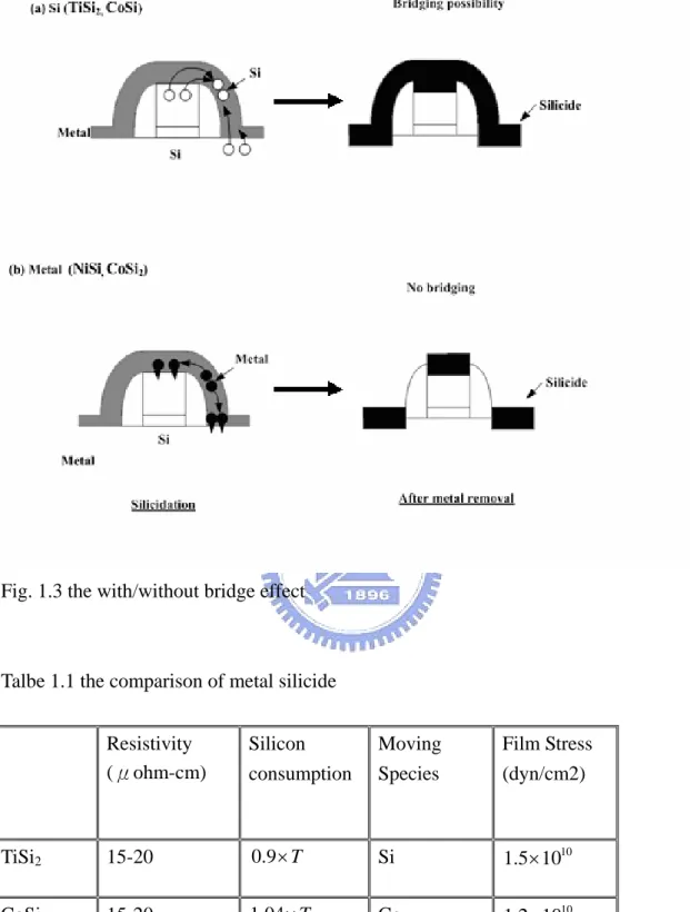
---27Fig. 1.3 the with/without bridge effect
---28Fig. 2.1 the process flow and top view of samples
---32Fig. 2.2 space charge distribution of the one-side abrupt junction
---34Fig. 2.3 plotting 1/C
2versus V
---34Fig. 3.1 Illustration of the dopant activation
---35Fig. 3.2 the SIMS measurement of heavily implanted sample (M/P
+/N junction)
---36Fig. 3.3 (a) I-V measurement and (b) effective doping density of M/P
+/N
---37Fig. 3.4 SIMS profile of heavily implanted phosphorous sample (M/N
+/P)
---38Fig. 3.5 (a) I-V measurement and (b) effective doping density of M/P
+/N
---39Fig. 3.6 (a) type 1 C-V distortion and (b)type 2 C-V distortion for the M/N
+/P
samples
---40Fig. 4.1 Reverse current density (I-V method) for lightly implanted M/P
+/N
----41Fig. 4.2 Only one kind of C-V distortion for lightly implanted M/P
+/N sample
treated at RTA 600℃(a) 120s and (b) 60s+60s(both linear junction like)
---42Fig. 4.3 Reverse current density (I-V method) for lightly implanted M/N
+/P
samples
---43Fig. 4.4 There are two kinds of C-V distortion for lightly implanted M/N
+/P
samples treated at RTA 600℃ (a) 120s (linear junction like) and (b)
60s+60s (hyper junction like)
---44CHAPTER 1
Introduction
1.1
General background
Transistor dimensions, including junction depths, are scaled aggressively each technology generation to sustain Moore’s Law, as showed in Fig. 1.1, enabling higher densities, better transistor performance, and increased functionality. When the pattern size of device continuously narrows, for MOS transistor, the thickness of the gate dielectric becomes too thin to operate under one voltage. When the device size less than 0.1 μm, we must use the high-K dielectric to replace the SiO2 being gate dielectric for the better performance (refer
to Fig. 1.2). Additionally, there are other problems at this generation, such as the short-channel effect, the high series resistance of the interconnection, and the shallow junction formation. To reduce the parasitic resistance of the source/drain contacts, a salicide process is required. The metal-silicide-related technology has become an integral part of sub-micro devices for reducing the parasitic resistance, which would improve the device and circuit performance.
Nowadays, the researches of the high-k material are popular. However, conventional technology for junction formation at source and drain requires high temperature process. It would affect the high-k materials, because the high-k materials will crystallize at high temperature [1]. In addition, high temperature activation process will prevent shallow junction formation at S/D. Because of above reasons, low temperature process is a trend. In this thesis, we study the mechanisms of shallow junction formation at the silicide/silicon interface, which combines the concept of implant into silicide (IIS) and solid phase epitaxial regrowth. Additionally, the materials of silicidation are also very important for the device
performance.
1.1.1 salicide technology
The incorporation of metal silicides is quite necessary as we meet the basic requirements for contact metallization: low specific resistivity, low contact resistivity to both n- and p- type silicon, high thermal stability and good processibility. For the various generations of MOS devices, the contacts technology have evolved from the so-called POLYCIDE (it means silicdes deposited on the poly-Si) to today’s standard salicides (self-salign silicided).
A salicide structure consists of a metal silicide formed atop the lines of polysilicon that make up the gates and the local interconnects, It is also form on the source/drain regions. The salicide on the source/drain regions can reduce the sheet resistance of the path between the metal contact and the channel edge. The salicide technology has an advantage that it can be formed without any extra mask. A salicide process is executed as follows [2]:
1. The metal which used to form the silicide is deposited on silicon.
2. The wafer is heated and the metal reacted with silicon to form the silicide
3. The unreacted metal is selectively removed by using an etchant that does not attract the silicide, the silicon substrate, and the SiO2. Then, the salicide process is
completed.
Among the metal silicides, TiSi2, CoSi2, and NiSi have been widely studied due to their
good thermal stability and low electrical resistivity. TiSi2 has been the most studied due to its
wide usage for CMOS metallization. CoSi2 began to replace the TiSi2 at a gate length of 0.25
μm and below. This replacement is due to increasing difficulties in forming low-resistivity TiSi2 as the dimension grew smaller. The CoSi2 technology is mature by now, however, it is
anticipated that NiSi will take over for CMOS technologies when gate length at 70 nm and below.
1.1.1.1 Titanium Silicide
TiSi2 is known to occur in two different crystallographic structures, C49 and C54 TiSi2,
and latter is a stable phase. Therefore, C54 TiSi2 is desired for the electronic devices, not only
due to its stability, but also due to the fourfold lower resistivity than C49 TiSi2, the resistivity
of C49 TiSi2 is around 60-80 μohm-cm, and that of C54 TiSi2 is only around 15-20μ
ohm-cm [2]. TiSi2 can reduce native oxide layers, making the TiSi2-contacted shallow
junction exhibits low contact resistance. When it is used being the gate electrode, it is an effective getter for the hydrogen atoms, and this improves the hot-electron reliability [3]. However, some drawbacks of Ti have been reported that Ti may react with the implanted dopant to form the metal compounds, and this will prevent the shallow junction formation [4]. The grain size of TiSi2 has to be larger than 0.2μm to achieved lower resistance. When the
gate line width is smaller than 0.2μm, TiSi2 application would be in trouble. And TiSi2 has
bridge effect (as show in Fig 1.3), the creep-up phenomenon during the formation of TiSi2
between the gate and the source/drain during annealing process, causing the device failure [5]. 1.1.1.2 Cobalt Silicide
CoSi2 is another attractive material for salicide process. The cobalt (Co) is transformed
to CoSi2 by a two step process. Co and Si are reacted to form CoSi at 450℃ first. After
removing the unreacted Co, a second thermal step at 700℃ is performed for the CoSi2
formation. The CoSi2 offers the benefits of lower resistivity, lower thermal budget, and higher
thermal stability than TiSi2. Furthermore, bridging effect is not a problem for CoSi2. But it
still has some disadvantages. Cobalt is very reactive and forms cobalt oxide easily when it contacts with air or moisture, so it often needs passivation layer. And the formation of CoSi2
consumes a relatively larger amount of Si to achieve an equivalent silicide sheet resistance than other silicides, as discussed in [3].
1.1.1.3 Nickel Silicide
In recent years, NiSi is another promising candidate to replace the CoSi2 for the
contact metal in submicron device applications. [6], some main advantages of NiSi are listed as follows:
1. NiSi has a lower formation temperature than TiSi2 or CoSi2.
2. NiSi has a low electrical resistivity. 3. NiSi has a low Si consumption.
4. NiSi also doesn’t have the creep-up phenomenon [7].
Because of the high solubility of Ni in Si, NiSi can be formed at low temperature(~400℃)[8] and low activation energy of about 1.5 eV [9]. NiSi has a slightly lower resistivity (10-15 μ ohm-cm) than both C54 TiSi2 and CoSi2 (15-20 μohm-cm) have. There are two reasons
contribute to the lower consumption of Si. First, the Si density of NiSi is lower than that of CoSi2, and this attribute makes the reduction for Si consumption more then 10%. Second,
because the resistivity of NiSi is lower than that of CoSi2, for the same sheet resistance, the
thickness of NiSi film can be thinner. NiSi can be formed at narrower poly lines than cobalt silicide is, and it doesn’t show a resistance increasing for narrow lines. All in all, NiSi film has the properties of low NiSi/Si contact resistance, wide process window (for example, even for a narrow Si line down to 100 nm width, NiSi can be formed at low annealing temperature 400℃ for 30 s [10]), and low film stress [11]. The main hurdle in using NiSi for contact metallization and local interconnection has been the poor thermal stability, if the NiSi suffered above 650℃, NiSi film might agglomerate which would produce leakage current [12]. Fortunately, the annealing temperature we adopt are below 650℃, the agglomerating problem of NiSi film can be ignored. Because of above reasons, NiSi film is the most suitable materials for our study. The comparison of the characterization of the Ti, Co and Ni is listed at Table 1.1.
1.1.2 Low Temperature Activation Technique
Because of the introduction of high-k materials in CMOS process, convention shallow junction formation technique isn’t suitable for this generation. Nowadays, there are three primary techniques for dopant activation at low temperature, which are solid phase epitaxial regrowth (SPER), implant into silicide (IIS), and diffuse silicide source (DSS). In our experiment, we combined the concepts of the SPER technique and IIS technique for our samples. So we will give a brief introduction for these two techniques.
1.1.2.1 Solid phase epitaxial regrowth (SPER)
When we use low temperature process for junction formation, the dopant activation is an important issue. In recent years, recrystallization of implanted amorphous silicon layer has been demonstrated for complete activation of dopants at lower temperature [13]. That is so-called SPER(Solid phase epitaxial regrowth) technique. SPER technique is pre-amorphous crystal silicon to amorphous type by implanting heavy ion, and Ge ion is often used be the implant ion. After the implantation for junction, the dopant almost remain in amorphous region and when annealing process is performed, dopant activation will be achieved a level above the equilibrium solid solubility during crystalline regrowth. For example, for the boron ion implanted into amorphous layer, during regrowth, dopant incorporation to substitutional sites is far higher than the equilibrium solid solubility at that temperature for the case of crystalline Si. This is likely due to a lower activation energy arising from the lack of a kick-out mechanism, as required in crystalline Si. The advantages of SPER are the suppression of channeling effect, the relative high dopant activation than conventional dopant activation, and compatibility with metal gate and high-k low thermal budget requirements. The thermal annealing is needed to recrystallize the amorphous layer and to electrically activate the dopant. And if the annealing temperature is high enough (above 700℃), it can recovery end-of-range (EOR) defects. The EOR defects are Is (self-interstitials) in excess precipitate forming extended defects, such as defect clusters and dislocation loops, which is
presented at the amorphous/crystalline interface during amorphization. 1.1.2.2 Implant into silicide (IIS)
The implant into silicide (IIS) technique is another alternative to fabricate the shallow junction with low thermal budget. In the IIS process, the dopants are implanted into the silicide, and then they diffused into the underlying substrate after activated annealing. This technique offers several advantages. First of all, the junction formed by IIS is almost free of implant damage and channeling effect, since the metal silicides have a larger nuclear stopping power than silicon has, the damages are almost confined in the silicide region. And the obtained junction is uniform to the silicide/silicon interface, this will reduce the possibility of junction penetration [14]. Finally, because of the dopant segregation phenomenon, the dopant will pile up at the silicide/silicon interface to form a high concentration profile, which results in low contact resistance. It has potential to form better ohmic contact. Since the low thermal budgets for IIS, it is suitable for the high-k material and the process of the sub-micro devices.
1.2
Motivation
When the device dimension scales down into the nano-device generation, the performance of CMOS has some problems such as gate-leakage and poly depletion. To conquer these problems, introduction of new materials is a tendency. Metal/high-k gate stack technology is a promising structure since it provides both low gate-leakage and minimal poly depletion effect [15]. For the high-k dielectric, hafnium based material is a promising candidate. But it can’t tolerate high temperature process, because it will crystallize at high temperature as description at section1.1. If the high-k dielectric is crystallized, the gate-leakage current will increase dramatically. Therefore, the thermal reliability of high-k dielectric is the main drawback need to be overcome. Since the thermal reliability is playing an important role for Metal/high-k gate stack technology, we use the NiSi as the contacting material due to its low temperature process window. Additionally, for the implant into silicide
(IIS) technique that NiSi is a good diffusion source has been purposed for formation of silicide contacted shallow junction.
Beside the low temperature of silicide formation, we hope the process temperature after gate dielectric formation can also be lower. We combine the concept of implant into silicide (IIS) and solid phase epitaxial regrowth (SPER) to control junction depth and junction activation. The IIS can minimize the implant damage and the SPER make the dopants which are in the amorphous silicon region active to a level above the equilibrium solid solubility during crystalline regrowth.
There are many studies showed that the PN junctions fabricated by IIS technique have good performance, such as low reverse current, low contact resistance, high activation energy [16], and been integrated in MOS device [17]. In our previous work, we successfully achieved high level activation at low temperature annealing ( around 450 ℃ ~650 ℃ ) [18,19]. Nevertheless, in the back-end thermal condition of CMOS processes, there are some thermal processes near around these temperatures, too. For example, a nitride layer is often used be the passivation layer to prevent phosphorus from PSG diffusing into the activation area, PECVD nitride deposited at temperature around 580℃. And forming gas annealing are often around 450℃.[20] How the post IIS thermal treatment affects the device’s performance is what we want to know. In our study, we introduced the additional thermal process after the junction formation which is done by IIS, and discussed the deactivation behavior of dopants.
The high activation level can be achieved at low temperature by using these techniques. And we want to know more information about shallow junction formation such as the thermal stability of device’s performance and the deactivation behavior of the dopants. The more details with our experiment will be discussed in the following chapters.
1.3
Organization of thesis
which is done by IIS technique. And we study the fabrication and characterization of the NiSi/ p+n and NiSi/ n+p samples.
In chapter1, it is brief introduction about metal silicide technology history, implant into silicide technique, solid phase epitaxial regrowth technique, and the motivation of this thesis.
In chapter2, it is the fabrication of the NiSi/ p+n and NiSi/ n+p shallow junction which
were done with the variation of dopant dose and annealing temperature.
In chapter3, it is the discussion of the electrical characterization of the NiSi/ p+n and
NiSi/ n+p shallow junction which were heavily implanted samples.
In chapter4, it is the discussion of the electrical characterization of the NiSi/ p+n and
NiSi/ n+p shallow junction which were lightly implanted samples.
In chapter5, It is conclusion and future work.
1.4
Reference
[1] C.S. Kang, H.J. Cho, R. Choi, Y.H. Kim C.Y. Kang, S.J. Rhee, C. Choi, M.S. Skbar, and J.C. Lee: Electron Devices, IEEE Transactions on, Vol. 51, Issue 2, Feb, 220, (2004). [2] R. Beyers and R. Sinclair: J. Appl. Phys. 57, 5240 ~1985 (1985).
[3] S. Wolf: ”Silicon Processing for The VLSI ERA”, second addition, Lattice Press, vol. 2,
Chapter 3, 2000.
[4] V. Probst, H. Schaber, P. Lippens, L. Van den hove and R. De Keersmacker: Appl. Phys.
Lett. 52 (1988) 1803.
[5] Y. Taur, J. Y. C Sun, D. Moy, L. K. Wang, B. Davari, S. P. Klepner and C. Y. Ting: IEEE
Trans. Electron Devices 34 (1987) 575.
[6] C. C. Wang, C. J. Lin and M. C. Chen: J. Electrochem. Soc. 150 (2003) G557.
[7] A. Lauwers, A. Steegen, M. de Potter, R. Lindsay, A. Satta, H. Bender and K. Maex: J. Vac.
[8] C. C. Wang, Y. K. Wu, W.H. Wu and M. C. Chen: Japan Society of Applied Physics Vol.
44 No. 1A, 2005, pp. 108~113.
[9] M.-A. Nicolet and S. S. Lau,in VLSI Electronics—Microstructure Sciences, edited by N. G.
Einsprich and G. B. Larrabee ~Academic, New York, 1983, Vol. 6, Chap. 6.
[10] T. Ohguro, et al: IEEE Trans, Electron Devices 41, 2305 (1994).
[11] T. Ohguro, S. Nakamura, M.Koike, T. Morimoto, A. Nishiymam, Y.Usihiku, T. Yoshitomi, M. Ono, M. Saito and H. Iwai: IEEE Trans. Electron Devices 41 (1994) 2305.
[12] C. C. Wang, and M. C. Chen: JJAP, Vol. 45, No. 3A, 2006, pp. 1582-1587. [13] M.Y. Tsai and B.G. Streetman: J. Appl. Phys. 50, 183(1979).
[14] F. La Via, C. Spinella, and E. Rimini: Semicond. Sci. technol, Vol. 10, P. 1362, 1995. [15]. Hobbs et al: Symp. VLSI tech., 9, 2003.
[16] Advanced Micro Devices, Inc. US Patent number-7306998.
[17] A. Kinoshita, C. Tanaka, K. Uchida and J. Koga: IEEE VLSI, 158,2005.
[18] K. M. Chang, J. H. Lin; C. H. Yang: Semiconductor Device Research Symposium, FP6-5,
2007.
[19] K. M. Chang, J. H. Lin, and Cheng-Yen Sun: Applied Surface Science, Vol 154, pp.
6151-6154, 2008.
[20] Hong Xiao: “Introduction to Semiconductor Manufacturing Technology”, international
Chapter 2
Device fabricated and theory of measurement
2.1 Introduction
For the traditional p-n junctions, it was form by implanting the ion into silicon substrate and then activated by high temperature furnace annealing. There are some drawbacks of conventional methods, such as channeling effect, high temperature dopant diffusion, and high thermal budget. These effects limit the shallow junction formation. Additionally, furnace annealing is not suitable for the commercial fabricated processes due to its low output. In recent years, low temperature activation technique is more important in nanometer regime. Many researches of advanced junction formation are performed, it includes the B4H10
implantation [1, 2], low energy implantation [3], gas-immersion laser doping (GIDL) [4, 5], implant into silicide (IIS) [6, 7, 8], and solid phase epitaxial regrowth (SPER) [9-11]. About low energy ion implantation, the major drawback of the method is that no commercial implantation system of such a low energy ion beam is available. And for the GILD technique, it eliminates the problems associated with ion implantation, and the unwanted diffusions that occur during activation process. However, GILD has issues of non-equilibrium phase transformations and high dependence of recrystallized structure on the applied energy density [12].
In this experiment, we adopt implant into silicide (IIS) and solid phase epitaxial regrowth (SPER), both techniques are discussed in chapter 1. They are potential processes for shallow junction formation. About the implant into silicide (IIS), the metal silicide has large nuclear stopping power than silicon due to the amorphous type of silicide, so it can effectively reduce the channeling effect. And it also reduces the damage of the implantation, due to the damage
is almost remained in the silicide region. For the solid phase epitaxial regrowth (SPER) technique, silicide/silicon interface has thin amorphous layer during silicidation process, it raise the dopant activation for shallow junction. Finally, to avoid the high dopant diffusion, we use the rapid thermal annealing (RTA) to replace the furnace annealing.
In our previous work, we studied the mechanism of implant into silicide technique, and we got some information, such like how the SPER affects the activation process, and achieving high level activation at low annealing temperature [13, 14]. The more information we want to know is the thermal stability of our devices. In our experiment, we adopt variation implant doses (heavily implanted samples and lightly implanted samples) and additional thermal processes after device formation (i.e. 3rd RTA and 4th RTA).
In this chapter, we investigate fabrication of NiSi/p+n and NiSi/n+p shallow junction with
different conditions discussed at above article. We would combine the dopant pile-up phenomena of IIS at interface and the ability of SPER to achieving the formation of shallow junction. We also introduce the theory of measurement. In our previous work, we got the samples we fabricated were abrupt junctions, so we adopt the abrupt junction physics theory in this thesis, such like I-V measurement and C-V measurement. Moreover, in order to realize the activation mechanism of implant into silicide technique, we introduced the SIMS (Secondary Ion Mass spectrometry) measurement. However, some samples in this experiment don’t show the characteristics of abrupt junctions, but the linear junctions, hyper junctions or otherwise. We will discuss about this phenomena.
2.2 experimental procedures
Samples are fabricated on n-type/p-type, (100)-oriented silicon wafers. After standard RCA cleaning, a 500nm field oxide was thermally grown by wet oxidation at 1000℃ for 90min. Active regions were defined by photolithography and etched by BOE (buffer solution etchant) solution. To reduce the series resistance of measurement, we have to form the ohmic
contact of backside of device, the backside of p/n type wafers were implanted with BF2+/P31+
at an energy of 20keV to a dose of 5×1015cm-2, followed activated annealing with 900℃
60sec by RTA system. Next, Stand clean was used again for removing the contamination. A nickel (Ni) film of 20nm thickness was deposited in Dual E-gun Evaporation system with a base pressure of less than 2×10⁻⁶ Torr, using a Ni target in vacuum ambient with a deposition
rate of about 0.08-0.12 nm/sec. After Ni film deposition, all samples were treated 1st RTA 400
℃ 30sec in N2 ambient to form nickel monosilicide (NiSi). And the unreacted Ni film was
selectively etched by a solution of H2SO4: H2O2=3:1 at 75-85℃ for 1min. After above steps,
the active regions and NiSi silicide were completed. Then the n+p and p+n junction diodes
were formed by P31+ implantation and BF2+ implantation into/through the NiSi silicide. The
P31+ implantation was performed at an energy of 20keV to a dose of 5×1013cm-2 (lightly
implanted sample) or a dose of 5×1015cm-2 (heavily implanted sample). And the BF2+
implantation was performed at an energy of 20keV to a dose of 5×1013cm-2 (lightly implanted
sample) or a dose of 5×1015cm-2 (heavily implanted sample ). Next, we deposited Ti on NiSi
with lift-off technique. First, we used photolithography to define the four-point probe measuring pads, and we deposited Ti 50nm by Dual E-gun Evaporation system (the condition of Ti deposition is the same with that of Ni deposition). After the Ti deposition, we removed PR by Acetone, and the Ti film was patterned. Then all samples were deposited TaN 150nm by ULVAC Sputter system with a base pressure of less than 6×10⁻⁷ Torr (the ambient gas ratio
is Ar : N2=19:1) on backside. Finally, followed by variation thermal annealing process (2nd
RTA: 400℃-650℃ for heavily implanted samples and 450℃-600℃ for lightly implanted samples, 50℃ per step) 60sec in a N2. For additional thermal process, heavily implanted
samples were added an extra 3rd RTA process and 4th RTA process at the same temperature
used in 2nd RTA. And lightly implanted samples were treated by 3rd RTA or longer 2nd RTA
(i.e. samples were treated by 2nd RTA 450℃-600℃ 120s) process. The fabricated processes
in Table 2.1 and Table 2.2.
2.3 Measurement system
We adopted the methods of Current-Voltage (I-V), Capacitance-Voltage (C-V) and Current-Temperature (I-T) to characterize the junction diodes. I-V and C-V characteristics of the junction diodes were measured using the semiconductor parameter analyzer HP-4156C and HP-4284, respectively.
2.4 Theory of measurement
2.4.1 SIMS measurementSecondary ion mass spectrometry is very powerful technique for the analysis of impurities in solids. The technique relies on removal of material from a solid by sputtering and on analysis of the sputtered ionized species. Most of sputtered materials consists of neutral atoms and cannot be analyzed. Only the ionized atoms can be analyzed by passing through an energy filter and a mass spectrometer. But SIMS determines the total impurity density, not the electrically active impurity density. Even it only affords the doping profiles, this is still very helpful for our experiment. For the electrically active impurity density, we adopted the C-V measurement.
2.4.2 C-V measurement
We adopted the capacitance-voltage measurement to analysis the junction interface. The measured capacitance consists of three parts in series, silicide/silicon capacitance, junction depletion capacitance and back contact capacitance. In silicide/silicon junction capacitance part, according to the literature [13], silicide/silicon junction had ohmic contact behavior. A high dopant concentration at M/S interface would result in large capacitance. So we can neglect the silicide/silicon capacitance term in our analysis. For the back contact capacitance, the area of the capacitance is almost about the full wafer size, it is bigger than that of abrupt
junction capacitance. Therefore, the capacitance of back contact can also be neglect in capacitance-voltage analysis. Consequently, the main measured capacitance is dominated by junction depletion capacitance. The depletion-layer capacitance per unit area is defined as
/ j
C =dQ dV , where Q is the incremental depletion charge on each side of the junction upon
an incremental charge with the applied voltage υ. The space charge distribution of the one-side abrupt junction is showed in Fig. 2.2. For one-side abrupt junctions, the capacitance per unit area is given by:
2 2( ) s s B j bi q N C kT W V V q ε ε = = − − (1) where V is positive/negative for forward/reverse bias, Rearrange the above Eq.(1):
2 2 2( ) 1 bi j s B kT V V q C q Nε − − = (2) it is clear from Eq.(2) that by plotting 1/C2 versus V, a straight line should result from a
one-side abrupt junction as shows in Fig. 2.3. The slope gives the impurity concentration of the substrate (NB), and when 1/C2=0, the medical point on x-axis means (Ψ −bi 2kT q/ ). Rearrange the above Eq.(2), we can obtain the impurity concentration at the depletion layer dege, as showed below:
2 2 ( ) [ ]. (1/ ) B s dV N W qε d C = (3) We know Ψ equation: bi 2
ln
A D bi iN N
kT
q
n
Ψ =
(4) Rearrange the above Eq.(4) which we can otain the interface doping density can be estimated as following [15]: 2 / biq kt i A Dn
N
e
N
Ψ=
for N-type (5)or 2 / biq kT i D A
n
N
e
N
Ψ=
for P-type (6) We obtained the electrically active impurity density by Eq.(5) and Eq.(6). We measured the C-V data by HP-4284, the measuring sweep voltage was from reverse bias to forward bias for N-sub and P-sub samples.2.4.3 I-V measurement
For directly determining the junction behavior, we used the I-V measurement to analysis the electrical characteristic of samples. The measuring sweep voltage was from forward bias to reverse bias for both type samples. From the I-V curve, we noticed the Joff (A/cm2) current
densities for both type samples. It exhibit the junction quality of the samples.
2.5 Reference
[1] M. A forad, R. Webb, R. Smith I. Jones, A. Al-Bayati, M. Lee, V. Agrawal, S. Banerjee, J. Matsuo and I. Yamada: 1998 International Conference on Ion implantation Technology
Proceedings, Vol. 1, p. 106, 1998.
[2] K. Goto, J. Mastuo, T. Sugii, H. Minakata, I. Yamada, and T. Hisatsugu: 1996
International Electron Devices Meeting, p. 435, 1996.
[3] S. Talwar, G. Verma, and K. H. Weiner: 1998 International Conference on Ion
Implantation Technology Proceedings, Vol. 2, p. 1171, 1998.
[4] P. G. Carey, K. H. Wiener, and Thomas W. Sigmon: IEEE Electron Device Letters, Vol. 9,
p. 542, 1988.
[5] E. Ishida and L. Larson: University/Convernment/Industry Microelectronics Symposium,
1995. , Proceedings of the Eleventh Biennial, p. 105, 1995.
[6] C. C. Wang, H. H. Lin, and M. C. Chen: Japanese Journal of Applied Physics, Vol. 43, No.
[7] C. C. Wang, Y. K. Wu, W. H. Wu and M. C. Chen: Japanese Journal of Applied Physics,
Vol. 44, No. 1A, 2005, pp. 108-113.
[8] C. C. Wang and M. C. Chen: Japanese Journal of Applied Physics, Vol. 45, No. 3A, 2006,
pp. 1582-1587.
[9] Pedro Lopez, Lourdes Pelaz, Luis A. Marques, Juan Barbolla, H, J. L Gossmann, Aditya Agarwal, Kenji Kimura, Tomoyoshi Matsushita: Materails Science and Engineering
B124-125 (2005) 379-382.
[10] Andrei I, Titov, Sergei O. Kucheyev: Nuclear Instruments and Methods in Physics
Research B 168 (2000) 375-388.
[11] Y. L. Chao, S. Prussin, and J. C. S. Woo: Applied Physics Letters 87, 142102 (2005) [12] G. Kerrien, J. Boulmer, D. Debarre, D. Bouchier, A. Grouillet, D. Lenoble: Appl. Surf, Sci,
186 (2002) 45.
[13] K. M. Chang, J. H. Lin; C. H. Yang: Semiconductor Device Research Symposium, FP6-5,
(2007)
[14] K. M. Chang, J. H. Lin, and Cheng-Yen Sun: Applied Surface Science, Vol 154, pp.
6151-6154, 2008.
[15] Donald A. Neamen: Semiconductor Physics and Devices, Third Edition, Chapter 7. [16] B. S. Chen and M. C. Chen: IEEE Trans. Electron Devices 43, 258, (1996).
Chapter 3
Heavily implanted samples
3.1 I-V and C-V measurement Results of M/P
+/N junction
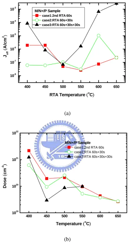
3.1.1 Brief introductionBefore the discussion of our experiment, we should know some information. According to our previous works [1, 2], SPER process is started from M/S interface into silicon substrate with temperature increasing (the illustration is showed in Fig.3.1). For the heavily implanted samples (M/P+/N), the SIMS measurement (refer to Fig.3.2) indicated the implantation peak is
in the silicon and the thickness of NiSi film is around 20nm. And we discovered that when the second annealing temperature is below 550℃, the activated behavior is dominated by SPER mechanism. Contrarily, if the temperature is above 550℃, bulk activation takes place. I-V and C-V measurement results of the device treated with three different thermal conditions (case 1: 2nd RTA 60sec, case 2: adding 3rd RTA 30sec after 2nd RTA, case 3: 4th RTA 30sec is added
after case 2, as showed in Table.2.2). 3.1.2 Analysis of M/P+/N junction
Fig.3.3 shows the I-V measurement and effective doping density extracted by C-V measurement of M/P+/N samples. The reverse bias current density is extracted at VR=2V and
divided by sample area. In case 1, the SPER process is likely completed at 2nd RTA
temperature 550℃ due to its highest on/off ratio than other samples (the more details are discussed in [1]). With temperature range below 550℃ in all cases, because the SPER process is not completed, the reverse bias current density decreases with the annealing temperature increasing in all cases. On the other hand, the reverse current is lowered with more RTA times
at that range. This is easy to explain: because the SPER process is continuous going, the more thermal treatment; the higher activation level (refer to Fig.3.3 (b)). When the RTA time increases, the PN junction towards the heavily doping region, the higher effective doping densities it activates, the lower defects if faces. As a result, the samples in case 3 have lower reverse current density than the samples in case 2 with the same temperature treatment. Also the samples in case 2 have better performance comparing to the samples in case 1 with the same annealing temperature. In all samples (case 1, 2 and 3), the devices in case 2 treated at RTA 550℃ have the lowest reverse current in this study. This might due to the SPER process is more close to the completion. Moreover, the leakage currents of samples in case 2 are lower than that of the samples in case 1 above 550℃. According to the literature [1], bulk activation dominated the samples above 550℃, due to the resistance dramatically decrease at that samples. The improvement of devices in case2 treated with higher temperatures (600℃ and 650℃) might due to the bulk activation and SPER process are simultaneously occur: When the bulk activation takes place, the SPER process continuously operates. Because the more RTA times, there are lower defects in the space charge region lead to the reverse current decrease in case 2. By the way, the junction position of samples in case 2 maybe is deeper than other samples (in case 1 and case 3) at 550℃, the bulk activation took place early, as showed at Fig. 3.3 (b). As a result, it implies that case 2 maybe is the best process condition for junction formation by IIS technique in our experiment. In case 3, reverse current dramatically increases above 550℃ and it is higher than that of samples in case 1. Some paper pointed that de-activation of dopant maybe occur at higher temperature [3], but in C-V measurement, the result doesn’t change too much. It might be explained that during longer annealing times (i.e. 60sec+30sec+30sec), some defects such like dislocations generated at these temperatures [2, 4].
3.2.1 Brief introduction
The SIMS measurement is showed in Fig. 3.4, it exhibits that the implantation peak is in the silicide layer for heavily implanted samples (M/N+/P). Therefore, in this series of M/N+/P
samples, the junction activation might be mainly affected by both silicide assisted dopant activation and SPER process (there was an amorphous layer in silicide/silicon interface). The additional thermal treatment of M/N+/P samples are the same with M/P+/N samples: case 1:
2nd RTA 60sec, case 2: adding 3rd RTA 30sec after 2nd RTA, case 3: 4th RTA 30sec is added
after case 2, also showed in Table.2.2. 3.2.2 Analysis of M/N+/P junction
I-V measurement and C-V measurement (effective doping density) of M/N+/P junction
are showed in Fig. 3.5. according to literature [1], in case 1, the devices treated by annealing temperature 550℃ got the best performance comparing to other samples, such that the lowest reverse current, the highest on/off ratio and the lowest resistance. We supposed that the SPER process is likely completed in the samples in case 1 at annealing 550℃, it is similar to M/P+/N samples. For samples in case 2, the reverse current densities are lower than that in
case 1 at lower temperatures. It is showed that the SPER process isn’t completion at lower temperature in case 1, the samples get lower leakage current with adding additional thermal treatment (i.e. more annealing time 30s). This can be extrapolated by some factors, such as the silicide/silicon interface recrystallized (i.e. junction re-growth and extending) and more impurities migrated into lattice sites (doping activation). In M/P+/N samples, case 2 (RTA
60s+30s) is the best condition of devices, but it is not the same in M/N+/P samples. The
samples in case 2 having the lowest leakage current at 550℃ is similar to case 1, but when the temperature above 550℃, the reverse current becomes worse in case 2 (it is also worse in case 3). The phenomenon is also discovered in the M/P+/N samples in case 3. It can be explained
that the defects in silicon are generated at these temperatures. For case 3 in M/N+/P samples, it
increases dramatically. This phenomenon can not be explained by defects formation, because defects often formed at higher temperatures. Even that defect formation induces leakage current increasing at 400℃ is true, this phenomenon should be discovered in M/P+/N samples, but we did not. This could be explained by dopnat de-activation. The lower temperature samples added; the lower solid solubility phosphorous has [5]. After long time annealing, the atoms which were already on lattice sites precipitate by super-saturation. The precipitation could induce defects formation near the junction interface to generate leakage current. Additionally, because of the higher active doping density of M/N+/P samples than that of
M/P+/N samples (as showed in Fig. 3.5 (b)), it makes the dopant de-activation of M/N+/P
samples easier to be observed than that of M/P+/N samples. Since above two factors, we only
found it in M/N+/P samples. Finally, for case 3, though it is not a good process condition for
samples due to its large leakage current, we still discover some information about the samples. The samples treated at 500℃ have the lowest reverse current in case 3. The SPER process seems to be completed at lower temperature with longer annealing time (in case 3).
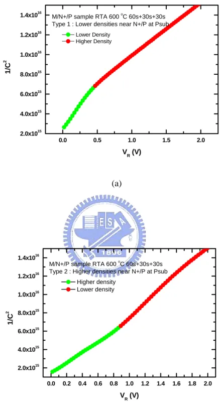
We found some C-V measurements of M/N+/P samples in case 3 were distorted. This is
implies some junctions have other kinds of junction behavior rather than abrupt junction. Two C-V distortions we found as showed in Fig. 3.6. Type 1 distortion (Fig. 3.6 (a)) has lower densities near N+/P interface at P-type substrate (it’s more like linear junction behavior rather than abrupt junction), and it is found in the samples treated at 600℃ and 650℃. Type 1 distortion could be understood by introducing the concern of dopant diffusion. When the samples experienced additional thermal process, phosphorous diffused into boron-doped substrate and activated. It would make the substrate counter-doped. Therefore, though the quantity of phosphorous which diffused into substrate is not a lot, it still affects the P side of M/N+/P when using C-V measurement method. Type 2 distortion (Fig. 3.6 (b)) has higher
densities near N+/P interface at P-type substrate (or hyper junction like behavior) and it is only
thermal process proceeding, the boron diffuse from substrate to M/S interface and pile up at the interface. After junction formation, if the position of junction is not deep enough, we will discover the type 2 distortion. However, if the assumption is true, the distortion should also be found at other samples. We will discuss about it. First, for M/P+/N samples, we didn’t
discover this phenomenon. This is might due to the implantation peak of boron is in the substrate (as showed in Fig. 3.2), so the pile up of the phosphorous is most in the P+ region
and is not significant in the N side. On the other hand, for M/N+/P samples, why do not all
samples have type 2 distortion? Although boron is faster diffuser than phosphorous under the same condition, but the implantation profile of phosphorous has a higher doping density gradient due to phosphorous is a heavier ion than boron, so phosphorous has a deeper diffused region. Therefore, in most case, the pile up of boron is most in the N+ region. However, when
the samples experienced the additional thermal annealing, phosphorous might be de-activated and the pile up of boron appears in the P side. As a result, the type 2 distortion takes place in these samples.
3.3 Reference
[1] K. M. Chang, J. H. Lin, C. H. Yang: Semiconductor Device Research Symposium, FP6-5,
(2007)
[2] K. M. Chang, J. H. Lin, C. Y. Sun: Applied Surface Science, Vol. 154, pp. 6151-6154,
2008.
[3] K. Larsen, V. Privitera, S. Coffa, F. Priolo, S. U. Campisano, and A. Carnera: physical
Review Letters, Vol. 76, No.9, pp. 1493, 1996.
[4] S. Wolf, and R. N. Tauber: ”Silicon processing for the VLSI era”, second edition, Lattice
press, Vol. 1, Chapter 10, 2000.
[5] S. Wolf, and R. N. Tauber: ”Silicon processing for the VLSI era”, second edition, Lattice
Chapter 4
Lightly implanted samples
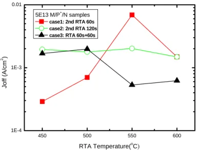
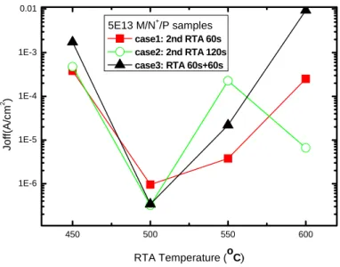
4.1 Brief introduction
In this chapter, we will discuss the thermal stability of lightly implanted samples. Interestingly, we discovered the thermal stability of lightly implanted samples is very different with that of heavily implanted samples. The process condition of samples was showed in Table. 2.1 and Table 2.2; the samples were formed by BF2+ implantation and P+ implantation
at an energy of 20keV to a dose of 5×1013cm-2. The thermal treatment conditions are showed
as follows: case 1: 2nd RTA 60s; case 2: 2nd RTA 120s; and case 3: added 3rd RTA 60s after
case 1.
4.2 I-V and C-V measurement results of M/P
+/N samples
Fig. 4.1 shows the reverse current with different RTA temperature of M/P+/N samples.
For case 1, it seems that the SPER process is best completed at 450℃ (more details were discussed at literature [1]), and leakage current increases with temperature increasing. The increasing of leakage current at 500℃ and 550℃ could be explained by the postulation of the dislocation formation of Si [2]. For case 2, the samples should suffer same high defect levels due to the little difference of leakage current of all samples. According to the C-V measurement, the junction formed by case 2 might be linear junction like, we extrapolate that after long annealing times (120sec), because boron is fast diffuser, the implantation profile distorted (more smooth). The gradient of impurity concentration is small, and the width of space charge region is wide. Therefore, the sample in case 2 has a little difference of leakage
current with each other. It seems that the case 2 is not the best process condition of junction formation. For case 3, the case 1 with 3rd RTA for 60s, the Joff becomes worse at 450℃ and
500℃. This is similar to that of heavily implanted samples, hence dopant de-activation which discussed in chapter 3 might be the reason. When the temperature increases, the leakage current gets improvement. The improvement might be contributed to the recovery of some defects which generated in the previous thermal treatments.
It is very different for C-V measurement results between lightly implanted samples and heavily implanted samples. In heavily implanted samples, the C-V distortion is founded only for M/N+/P samples treated at case 3 above 600℃. However, in lightly implanted samples, the abrupt junction behavior is hold only for M/P+/N samples treated at case 1. The C-V distortion of samples treated at case 2 and case 3 are showed in Fig. 4.2, there is only one kind C-V distortion (linear junction behavior like) for lightly implanted samples. It is similar to the type 1 distortion for heavily implanted samples. When the thermal treatment proceeded, the implanted carriers not only diffused from P+ to N region but also activated there. According to
the thermal condition of C-V distortion for lightly implanted samples and heavily implanted ones, this C-V distortion is easy to be found with a long-term thermal treatment.
4.3 I-V and C-V measurement results of M/N
+/P samples
The plot of reverse current versus RTA temperature is showed in Fig. 4.3. It exhibits obviously that the annealing temperature 500℃ is the best thermal condition for M/N+/P
samples in each case. Additionally, dopant de-activation under and defect generation above 500℃ lead the Joff increasing is similar to the results of the heavily implanted samples. And
the samples treated at 600℃ in case 3, the recovery of defects is observed. As a result, we can conclude that thermal treatment at 500℃ is the widest process window for M/N+/P
samples.
type 2 distortion (as showed in Fig. 4.4) that we met in heavily implanted samples. The linear junction like behavior (as showed in Fig. 4.4 (a)) is most found in the samples treated by case 2 and case 3 (except for 600℃). We thought that dopant diffusion and counter-doped might be the reason for type 1 distortion as discussed in previous chapter. And the hyper junction like behavior (as showed in Fig. 4.4 (b)) is only found in the samples treated in case 3 for 600℃. interestingly, type 2 distortion is found in M/N+/P samples (both heavily implanted samples
and lightly implanted ones) treated at 600℃ for 120s (120sec or 60+30+30sec). It might imply that the activation behavior of phosphorous is the main influence for type 2 distortion, such like the diffusion coefficient and other physical characterizations of phosphorous.
Comparing with heavily implanted samples and lightly implanted samples, we got the lightly implanted samples are more unstable than heavily implanted samples. This is might due to low dose implantation has more un-uniform impurity distribution, slower diffusing speed and faster activated rate, leading to un-uniform junction behavior (linear junction behavior, hyper junction behavior or otherwise).
4.4 Reference
[1] K. M. Chang, S. C. Lin: “Research of low temperature dopant activation at nickel silicide
and silicon interface using implant into silicide”, NCTU the thesis of master, 2008.
[2] S. Wolf, and R. N. Tauber: ”Silicon processing for the VLSI era”, second edition, Lattice
Chapter 5
Conclusions and Future Work
In our experiment, we studied the research of the thermal stability of heavily implanted samples and lightly implanted samples. For M/P+/N samples of heavily implanted ones, the
annealing temperature 550℃ for 90s was the best condition for junction formation. For M/N+/P samples of heavily implanted ones, it also had the best performance of leakage
current at annealing temperature 550℃. When samples experienced the case 3 condition (60+30+30sec), the dopant de-activation phenomenon was found at 400℃ due to low solid solubility and long annealing time. As a result, when temperature above 550℃, the defect formed in Si itself dominated the leakage current, on the other hand, the dopant de-activation dominated the leakage current below 550℃. And this extrapolation was also met in lightly implant samples. There were two C-V distortions in our experiment. Type 1 distortion is linear junction like behavior, and it was obviously discovered in long annealing terms. The origin of this distortion can be contributed that the implanted ions diffused into the lightly doped side of junction and induced the counter-doped. Type 2 distortion was only found at M/N+/P samples at 600℃, it seemed to imply that the implanted phosphorous is a key point of
this distortion. The distortion which had hyper junction like behavior is might due to dopant segregation effect, and is related to the substrate and implanted dopant characteristics such as diffusion coefficient and dopant de-activation. Finally, we discovered that lightly implanted samples had less thermal stability, since its less uniform dopant distribution than heavily implants ones. The performance of samples in case 2 is very different with that of samples in case 3, it exhibited that even at the same annealing time and temperature, the dopant activation behavior and defect distribution are different to each other. Additionally, not only
the annealing time affected performance lot, but also the heating and cooling time is very importance for shallow junction formation.
In order to improve our experiment, getting the optimum process condition is necessary. According to above article, we should study the best thermal condition, it included the heating time, annealing time, cooling time and optimum temperature. And we can use Spread Resistance Profile (SRP) to check the dopant activation and junction depth. According to the actual value, we could know whether our fabricated junction is shallow junction or not. As long as the dopant activation and leakage current level can achieve our expectation at low temperature process, we can replace the high temperature fabrication.
Fig 1.1 Moore’s law.
Fig. 1.3 the with/without bridge effect
Talbe 1.1 the comparison of metal silicide
Resistivity (μohm-cm) Silicon consumption Moving Species Film Stress (dyn/cm2) TiSi2 15-20 0.9 T× Si 1.5 10× 10 CoSi2 15-20 1.04 T× Co 1.2 10× 10 NiSi 10-15 0.82 T× Ni 9 6 10×
P-type/N-type (100) Si sub
RCA clean
P-type/N-type (100) Si sub
Thermal Wet Oxidation 300nm
SiO
2300nm
300nm
SiO
2P-type/N-type (100) Si sub
Define active area region
(300μm x 300μm)
P-type/N-type (100) Si sub
Back contact BF2/Phosphorous Implantation And Annealing SiO2Ni film 20nm deposited by
E-gunP-type / N-type (100) Si sub. SiO2 SiO2 Silicidation by 1st RTA (400℃ 30s)
Selectively etch
(H2SO4 : H2O2 = 3 : 1 ) 60 sec for unreact NiP-type / N-type (100) Si sub. SiO2 SiO2
Phosphorous/BF2
implantation
for
junction formation
P-type / N-type (100) Si sub.SiO2 SiO2
NiSi
Ti film 50nm deposited by
E-gun after coat PR
next to remove PR. (lift-off)
P-type / N-type (100) Si sub.
SiO2 SiO2 NiSi N+/P and P+/N Ti PR PR TaN 150nm deposited at backside by Sputter.
P-type / N-type (100) Si sub.
SiO2 SiO2
NiSi
N+/P+ and P+/N+
Ti
Fig. 2.1 Process flow and top view of samples Activation and Junction formation by 2nd RTA
P-type / N-type (100) Si sub.
SiO2 SiO2 NiSi N+/P+ and P+/N+ Ti TaN
SiO
2Ti
Top View
Fig2.2 space charge distribution of the one-side abrupt junction -2.0 -1.5 -1.0 -0.5 0.0 0.5 1.0 1.5 2.0 Slope α 1/Ν Voltage (volt) 1/C2 Vintercept=ψbi-2kT/q
Fig.2.3 plotting 1/C2 versus V
-+
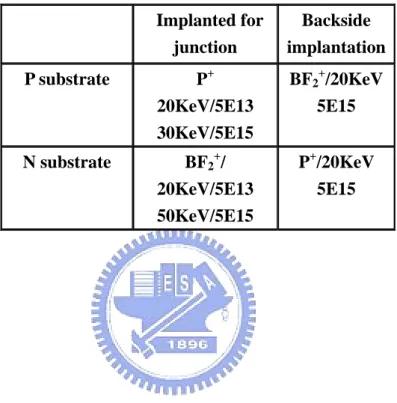
ρ P+ N +eNd -xp -eNa +xnTable 2.1 the implantation condition Implanted for junction Backside implantation P substrate P+ 20KeV/5E13 30KeV/5E15 BF2+/20KeV 5E15 N substrate BF2+/ 20KeV/5E13 50KeV/5E15 P+/20KeV 5E15
Table.2.2 the annealing process conditions
1st RTA 2nd RTA 3rd RTA 4th RTA Heavily implanted sample 400℃/30 sec 400℃-650℃ 60 sec (Case1) 400℃-650℃ 30 sec (Case2) 400℃-650℃ 30 sec (Case3) Lightly implanted samples 400℃/30 sec 450℃-600℃ 60 sec/120sec (Case1/2) 450℃-600℃ 60 sec (Case3)
Fig.3.1 Illustration of dopant activation. The P/N junction interface becomes deeper away from M/S interface with 2nd RTA temperature.
Dopant distribution
N
i
S
i
S
u
b
.
N
i
S
i
S
u
b
.
Junction
interface
Lower annealing temperatureN
i
S
i
S
u
b
.
Higher annealing temperature0 20 40 60 80 100 1E19 1E20 1E21 1E22 B o ro n C oncentr ation (cm -3 ) Depth (nm) MS interface Projection Range With 2nd RTA 650oC 60s
400 450 500 550 600 650 10-9 10-8 10-7 10-6 M/P+/N Sample case1:2nd RTA 60s case2:RTA 60s+30s case3RTA 60s+30s+30s Joff ( A/ cm 2 ) RTA Temperature (oC) (a) 400 450 500 550 600 650 1016 1017 1018 1019 M/P+/N Sample case1:2nd RTA 60s case2:RTA 60s+30s case3:RTA 60s+30s+30s Do p in g Den s it y ( cm -3 ) Temperature (o C) (b)
400 450 500 550 600 650 10-8 10-7 10-6 10-5 10-4 10-3 M/N+/P Sample case1:2nd RTA 60s case2:RTA 60s+30s case3:RTA 60s+30s+30s J off ( A/cm 2 ) RTA Temperature (oC) (a) 400 450 500 550 600 650 1019 1020 1021 1022 M/N+/P Sample case1:2nd RTA 60s case2:RTA 60s+30s case3:RTA 60s+30s+30s D o se ( cm -3 ) Temperature (o C) (b)
0.0 0.5 1.0 1.5 2.0 2.0x10¹⁵ 4.0x10¹⁵ 6.0x10¹⁵ 8.0x10¹⁵ 1.0x10¹⁶ 1.2x10¹⁶ 1.4x10¹⁶ 1/ C 2 V R (V) Lower Density Higher Density M/N+/P sample RTA 600 oC 60s+30s+30s Type 1 : Lower densities near N+/P at Psub
(a) 0.0 0.2 0.4 0.6 0.8 1.0 1.2 1.4 1.6 1.8 2.0 2.0x10¹⁵ 4.0x10¹⁵ 6.0x10¹⁵ 8.0x10¹⁵ 1.0x10¹⁶ 1.2x10¹⁶ 1.4x10¹⁶ M/N+/P sample RTA 600 oC 60s+30s+30s Type 2 : Higher densities near N+/P at Psub
1/ C 2 V R (V) Higher density Lower density (b)
450 500 550 600 1E-4 1E-3 0.01 Jo ff (A/cm 2 ) RTA Temperature(oC) 5E13 M/P+/N samples case1: 2nd RTA 60s case2: 2nd RTA 120s case3: RTA 60s+60s
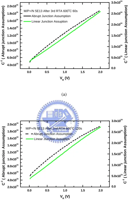
0.0 0.5 1.0 1.5 2.0 4.0x10¹⁵ 6.0x10¹⁵ 8.0x10¹⁵ 1.0x10¹⁶ 1.2x10¹⁶ 1.4x10¹⁶ 1.6x10¹⁶ 1.8x10¹⁶ 2.0x10¹⁶ 0.0 5.0x10²³ 1.0x1024 1.5x1024 2.0x1024 2.5x1024 3.0x1024 C -3 ( Li n ear j u ncti on Assu mpti on ) C -2 ( Ab ru pt j unc tion As s um pt ion ) V R (V)
Abrupt Junction Assumption M/P+/N 5E13 After 3rd RTA 600oC 60s
Linear Junction Assuption
(a) 0.0 0.5 1.0 1.5 2.0 2.0x10¹⁵ 4.0x10¹⁵ 6.0x10¹⁵ 8.0x10¹⁵ 1.0x10¹⁶ 1.2x10¹⁶ 1.4x10¹⁶ 1.6x10¹⁶ 1.8x10¹⁶ 2.0x10¹⁶ 0.0 5.0x10²³ 1.0x1024 1.5x1024 2.0x1024 2.5x1024 3.0x1024 C -2 ( Ab ru pt jun c tion Assump tion ) C -3 ( Lin e a r j unc tion As s um pt ion )
Abrupt Junction Assumption
V
R (V)
Linear Junction Assuption
M/P+/N 5E13 After 2nd RTA 600oC 120s
(b)
Fig. 4.2 Only one kind of C-V distortion for lightly implanted M/P+/N sample treated at RTA 600℃ (a) 120s and (b) 60s+60s (both linear junction like)
450 500 550 600 1E-6 1E-5 1E-4 1E-3 0.01 J o ff (A /c m 2 ) RTA Temperature (oC) 5E13 M/N+/P samples case1: 2nd RTA 60s case2: 2nd RTA 120s case3: RTA 60s+60s
0.0 0.5 1.0 1.5 2.0 2.0x10¹⁵ 4.0x10¹⁵ 6.0x10¹⁵ 8.0x10¹⁵ 1.0x10¹⁶ 0.0 2.0x10²³ 4.0x10²³ 6.0x10²³ 8.0x10²³ 1.0x1024 1.2x1024 1.4x1024 VR (V) C -3 ( L in ear j u ncti on Assu mpti on )
Abrupt Junction Assumption
C -2 ( Ab ru pt j unc tion As s u m pt ion )
Linear Junction Assuption
M/N+/P 5E13 After 2nd RTA 600oC 120s
(a) 0.0 0.5 1.0 1.5 2.0 3x10³ 4x10³ 5x10³ 6x10³ 7x10³ 8x10³ 9x10³ 0 1x10¹⁵ 2x10¹⁵ 3x10¹⁵ 4x10¹⁵ 5x10¹⁵ 6x10¹⁵ 7x10¹⁵
Hyper Junction Assumption
C -2 ( Ab ru pt j unc tion As s um pt ion ) C 1/ 2 ( H y p e r Ju nc ti on As s u m pt ion) V R (V)
M/N+/P 5E13 After 3rd RTA 600oC 60s
Abrupt Junction Assumption
(b)
Fig. 4.4 There are two kinds of C-V distortion for lightly implanted M/N+/P samples treated at RTA 600℃ (a) 120s (linear junction like) and (b) 60s+60s (hyper junction like)
姓 名:林 詩 帆 性 別:男 出生日期:民國七十二年十月十二日 出 生 地:台灣省新竹市 住 址:新竹市民生路 215 號 學 歷:國立中興大學物理學系 (民國九十二年八月~民國九十五年六月) 國立交通大學電子工程學系電子工程研究所碩士班 (民國九十五年八月~民國九十七年八月) 碩士論文: 以離子植入矽化物技術製作在矽化鎳與矽介面間形成陡峭接面之熱穩 定度相關研究
Research of Thermal Stability of Shallow Junction between Nickel Silicide and Silicon using Implant into Silicide Technique

![Fig. 3.4 SIMS profile of heavily implanted phosphorous sample (M/N + /P) [1]](https://thumb-ap.123doks.com/thumbv2/9libinfo/8134458.166370/48.892.226.709.168.541/fig-sims-profile-heavily-implanted-phosphorous-sample-m.webp)