Observation of 394 nm electroluminescence from low-temperature
sputtered n-ZnO / SiO
2thin films on top of the p-GaN heterostructure
Cheng Pin Chen, Min Yung Ke, Chien Cheng Liu, and Yuan Jen Chang
Graduate Institute of Electro-Optical Engineering, National Taiwan University, 1 Roosevelt Road, Section 4, Taipei 106, Taiwan and Department of Electrical Engineering, National Taiwan University, 1
Roosevelt Road, Section 4, Taipei 106, Taiwan Fu Hsiang Yang
Aixtron Taiwan Co., Ltd., 2F, No. 5, Lane 91, Dong Mei Road, HsinChu 300, Taiwan Jian Jang Huanga兲
Graduate Institute of Electro-Optical Engineering, National Taiwan University, 1 Roosevelt Road, Section 4, Taipei 106, Taiwan and Department of Electrical Engineering, National Taiwan University, 1
Roosevelt Road, Section 4, Taipei 106, Taiwan
共Received 7 June 2007; accepted 8 August 2007; published online 27 August 2007兲
The authors report on the 394 nm UV light emission from low-temperature sputtered n-ZnO / SiO2 thin films on top of the p-GaN heterostructure. They compare samples with and without a SiO2 current blocking layer. With a SiO2 layer, electroluminescence spectrum shows a sharp emission peak at 394 nm, which is attributed to the recombination of accumulated carriers between n-ZnO / SiO2 and p-GaN / SiO2 junctions. As for the sample without a SiO2 layer, a broadband ranging from 400 to 800 nm is observed, which is due to Mg+ deep-level transition in the GaN along with defects in the ZnO layers. © 2007 American Institute of Physics.
关DOI:10.1063/1.2777175兴
ZnO, with a large direct band gap of 3.37 eV, is a prom-ising material for ultraviolet共UV兲 light emissions or photo-detections. It possesses unique characteristics such as a large exciton binding energy of 60 meV共versus 26 meV for GaN兲, easy processing due to amenability to conventional chemical wet etching, and the possibility of low-temperature growth. Up to the present, heterostructure light emitting diodes 共LEDs兲 have been demonstrated by growing n-type ZnO on top of a variety of p-type layers such as GaN, Si, SrCu2O2, etc.1–4 Moreover, even though the development of high-quality p-type epitaxial growth for p-type ZnO is relatively slow, p-n ZnO diodes have also been realized.5
Several different emission wavelengths of ZnO hetero-structure LEDs have been presented, ranging from UV emis-sion at 375– 389 nm to wideband spectra 共violet-white to blue-white兲.6
For example, Alivov et al. compared growth of n-ZnO : Ga by chemical vapor deposition 共CVD兲 on both p-GaN : Mg/ c-Al2O3 and p-Al0.12Ga0.88N : Mg/ 6H-SiC structures.1,7 The wavelength maximum is 430 nm for ZnO / GaN LEDs and 389 nm for ZnO / AlGaN devices. It was inferred that electron injection from the n-ZnO into the p-GaN should be more energetically favorable than hole in-jection from the p-GaN into n-ZnO, while hole inin-jection from p-AlGaN into n-ZnO will be more favorable than elec-tron injection from n-ZnO into p-AlGaN.8Furthermore, Jiao et al.9fabricated n-ZnO / p-GaN diodes with a MgO layer for electron blocking. The result showed a peak wavelength at 380 nm.
Despite excellent results of UV light emission from pvious studies of ZnO / GaN based heterostructures, most re-cent studies have focused on carrier recombinations in the ZnO layer. Therefore, in addition to efficient current
block-ing structures, various growth methods were employed to achieve quality ZnO epitaxy for sharp excitonic emission peaks.6In this work, we demonstrate a 394 nm UV electrolu-minescence共EL兲 light emission from a n-ZnO/SiO2/ p-GaN heterostructure. Photoluminescence共PL兲, current-voltage di-ode curves, and EL measurement were conducted to charac-terize ZnO / GaN LEDs with and without a SiO2 current blocking layer.
The fabrication started from the preparation of a p-type GaN epiwafer. The p-type GaN layer was grown on top of a sapphire substrate by metal-organic CVD 共MOCVD兲. The effective carrier concentration in this layer is approximately 5⫻1017cm−3 after p-GaN activation. In the next step, a 300⫻300m2patterned SiO2layer was coated on top of the p-GaN layer at room temperature, followed by the deposition of a 300 nm heavily doped n-type ZnO at 100 ° C, both by rf magnetron sputtering. The 3 nm SiO2 layer is inserted be-tween p- and n-type layers for carrier blocking. We also pre-pared a LED sample without a SiO2 layer for comparison. The sputter target of the n-type ZnO was doped with 0.5 wt % Ga, and the ZnO layer was annealed at 550 ° C for 30 min after deposition. Finally, Ni/ Au and Ti/ Au were evaporated as the p-type and n-type contact electrodes, re-spectively. They were alloyed for optimum contact condi-tions.
We first perform room temperature PL measurement on a sputtered n-ZnO thin film as well as a p-GaN sample by a He–Cd laser operating at 325 nm. As shown in Fig.1, the PL spectrum of the n-ZnO shows a near-band-edge共NBE兲 emis-sion at 379 nm and a wide green band at 503 nm. Green luminescence has been reported to be due to oxygen vacancy related defects in the crystallite surface.10 Despite the fact that the intensity ratio between defect related and NBE emis-sion is higher than other approaches such as pulsed laser deposition or CVD due to the low-temperature sputtering
a兲Author to whom correspondence should be addressed; FAX: 886-2-2367-7467; electronic mail: [email protected]
APPLIED PHYSICS LETTERS 91, 091107共2007兲
0003-6951/2007/91共9兲/091107/3/$23.00 91, 091107-1 © 2007 American Institute of Physics
process, the sharp excitonic peak at 379 nm suggests that the material property is suitable for light emitting devices. In contrast, the PL spectrum of the p-GaN film reveals an in-tense deep-level emission at around 430 nm, which can be attributed to the transmission from the conduction band or shallow donors to the Mg acceptor doping level.11
Figure2shows the I-V curves of heterojunction devices with and without a SiO2current blocking layer. Both samples demonstrate a nonlinear rectifying behavior while an addi-tional voltage drop across the SiO2 layer is observed from the n-ZnO / SiO2/ p-GaN device. The large threshold voltage of both samples is related to the Schottky barrier between the contact electrode and the ZnO layer. EL spectra of these two devices are shown in Figs.3共a兲and 3共b兲, respectively. For the LED without a current blocking layer, a wideband emis-sion between 400 and 800 nm can be seen. By comparing the EL curves in Fig.3共a兲with PL spectra in Fig.1, the emission peaks between 421 and 438 nm result from deep-level carrier recombination in the p-GaN layer, while long tails are due to oxygen vacancies in the n-ZnO layer. As the injection cur-rent is increased, a blueshift is noted which is related to band filling in the p-GaN layer.12 As for the EL spectra of the sample with a SiO2layer, the emission maximum starts from 421 nm at a low injection current 5 mA, which, by compar-ing with the spectra in Figs.1and3共a兲, indicates that recom-bination occurs in the p-GaN layer. When we further
raise the bias voltage to a point that enough electrons and holes accumulate in the interface of n-ZnO / SiO2 and p-GaN / SiO2, respectively, recombination between n-ZnO and p-GaN by carriers through the SiO2can be found from the EL peak at 394 nm. Therefore, the emission peak shifts from 421 nm at 5 mA to 394 nm at injection currents above 10 mA. No significant wavelength shift can be observed for currents beyond 10 mA.
The emission at an optical energy lower than the NBE of ZnO can be described from the band diagram constructed from Anderson model. In Fig.4, the energy barrier for⌬EC and⌬EV in the interface of ZnO / SiO2 and GaN / SiO2, de-termined from electron affinity and band gap, is 3.24 and 2.5 eV, respectively. Therefore, the EL emission peak is shifted toward a longer wavelength due to the band offset at FIG. 1. PL spectra of rf sputtered n-ZnO共solid line兲 and MOCVD grown
p-GaN共dashed line兲.
FIG. 2. I-V curves of a n-ZnO / p-GaN LED共solid line兲 and a n-ZnO/SiO2 共3 nm兲/p-GaN LED 共dashed line兲.
FIG. 3. EL spectra of a ZnO–GaN LED 共a兲 and a n-ZnO/SiO2 共3 nm兲/p-GaN LED 共b兲. The bias current ranges from 5 to 30 mA at a step 5 mA.
FIG. 4. Band gap diagram of the n-ZnO / SiO2/ p-GaN structure.
091107-2 Chen et al. Appl. Phys. Lett. 91, 091107共2007兲
the valence of p-GaN. The result implies that with the inser-tion of a current blocking layer, the emission wavelength can be controlled by selecting different band gap structures of both the n-type and p-type layers.
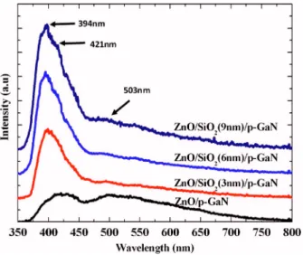
We further extend the thickness of SiO2layers to 6 and 9 nm. Figure5demonstrates the EL spectra of samples with 0, 3, 6, and 9 nm thickness of SiO2layers biased at an injec-tion current of 20 mA. All the samples have the same layout structure and p-type mesa area of 300⫻300m2. It is shown that the emission maximum occurs at 394 nm for the sample with a blocking layer and at 421 nm for the n-ZnO / p-GaN sample. Also, we have noticed that the rela-tive intensity of the n-ZnO / p-GaN sample is much weaker than that of samples with the SiO2 layer. The quantum effi-ciency, calculated from the EL spectra at 20 mA, of sample with 3, 6, and 9 nm SiO2is 7.6%, 24.5%, and 57.2%, respec-tively, higher than that of a n-ZnO / p-GaN device. It indi-cates that the SiO2layer helps confine carriers for the recom-bination between junctions of n-ZnO / SiO2 and SiO2/ p-GaN, and, thus, less carriers are consumed in the n-ZnO or p-GaN layer despite subpeaks at 421 and 503 nm
can still be observed for devices with SiO2. By comparing the EL spectra of the device without SiO2, those humps are related to carrier recombination in the n-ZnO and p-GaN layers. In this experiment, we also fabricated a sample with 12 nm SiO2 layer. But unfortunately the required bias volt-age is too large to be of practical measurement.
In conclusion, we fabricated a n-ZnO / SiO2/ p-GaN light emitting diode with 394 nm UV light emission. We compare samples with and without a SiO2current blocking layer. With a SiO2 layer, EL spectrum shows a sharp emission peak at 394 nm. The 394 nm peak is attributed to the recombination of accumulated carriers between n-ZnO / SiO2 and p-GaN / SiO2 junctions. As for the sample without a SiO2 layer, only the 400– 800 nm broadband is observed, which is due to Mg+ deep-level transition in the GaN and defects related recombination in the ZnO layers
This work was supported by the National Science Coun-cil of Taiwan under Grant No. NSC-95-2221-E-002-272.
1Ya. I. Alivov, J. E. Van Nostrand, D. C. Look, M. V. Chukichev, and B. M. Ataev, Appl. Phys. Lett. 83, 2943共2003兲.
2Qing-Xuan Yu, Bo Xu, Qi-Hong Wu, Yuan Liao, Guan-Zhong Wang, Rong-Chuan Fang, Hsin-Ying Lee, and Ching-Ting Lee, Appl. Phys. Lett.
83, 4713共2003兲.
3Peiliang Chen, Xiangyang Ma, and Deren Yang, J. Appl. Phys. 101, 053103共2007兲.
4Hiromichi Ohta, Masahiro Orita, Masahro Hirano, and Hideo Hosono, J. Appl. Phys. 89, 5720共2001兲.
5J.-H. Lim, C.-K. Kang, K.-K. Kim, I.-K. Park, D.-K. Hwang, and S.-J. Park, Adv. Mater.共Weinheim, Ger.兲 18, 2720 共2006兲.
6D. C. Look, B. Claflin, Ya. I. Alivov, and S. J. Park, Phys. Status Solidi A
201, 2203共2004兲.
7Ya. I. Alivov, E. V. Kalinina, A. E. Cherenkov, D. C. Look, B. M. Ataev, A. K. Omaev, M. V. Chukichev, and D. M. Bagnall, Appl. Phys. Lett. 83, 4719共2003兲.
8D. J. Roger, F. Hosseini. Teherani, A. Tasan, K. Minder, P. Kung, and M. Razeghi, Appl. Phys. Lett. 88, 141918共2006兲.
9S. J. Jiao, Y. M. Lu, D. Z. Shen, Z. Z. Zhang, B. H. Li, J. Y. Zhang, B. Yao, Y. C. Liu, and X. W. Fan, Phys. Status Solidi C 3, 972共2006兲. 10S. A. Studenikin, Nickolay Golego, and Michael Cocivera, J. Appl. Phys.
84, 2287共1998兲.
11M. A. Khan, Q. Chen, R. A. Skogman, and J. N. Kuznia, Appl. Phys. Lett.
66, 2046共1995兲.
12M. Asif Khan, Q. Chen, R. A. Skogman, and J. N. Kuznia, Appl. Phys. Lett. 66, 2046共1995兲.
FIG. 5. EL spectra of n-ZnO / SiO2/ p-GaN LEDs with different SiO2 thick-nesses. The bias current is 20 mA. The EL intensity is expressed in linear scale.
091107-3 Chen et al. Appl. Phys. Lett. 91, 091107共2007兲