Nonuniform Carrier Trapping among Quantum Dots
Yi-Shin Su, Wei-Che Chang and Ching-Fuh Lin
1Graduate Institute of Electro-Optical Engineering
1also with Department of Electrical Engineering and Graduate Institute of Electronics Engineering
National Taiwan University Taipei 106, Taiwan ROC
Abstract — In quantum-dot (QD) structures, carriers do
not distribute uniformly among QDs. Carriers tend to distribute at larger QDs. Combined with state filling effect, carrier will populate larger QDs first. Then, carrier will populate smaller QDs at higher injection density. The nonuniform carrier distribution also leads to the separation of two emission peaks with increasing current. On the fabricated devices, the photon energy difference between the two peaks increased from 70.8meV at 60mA to 78meV at 160mA. By observing the peak separation, the tendency of carrier distribution can be identified.
Index Terms — InAs quantum dot, broadband
semiconductor amplifier, semiconductor devices, nonuniform carrier distribution, quantum dot.
I. INTRODUCTION
Quantum dot (QD) devices have the advantage of high differential gain, low threshold current and improved efficiency [1] because they are supposed to have the unique delta function like density of states. However, growing single-size QDs is difficult. On the other hand, some researchers take advantage of the size fluctuation of QDs and demonstrate tunable lasers with more than 200nm tuning range [2]. In this case, the distribution of carriers among QDs becomes important. Nonuniform carrier distribution encountered nonidentical MQWs usually occur, so broadband devices using nonidentical MQWs cannot be easily achieved[3]. In comparison, Because QDs are distributed in the 2-D epi-growth plane, it is easier to obtain better uniformity of carrier distribution among QDs for broadband applications. However, the carrier distribution among QDs is still not really uniform. When the QDs do not have a single size, their corresponding quantized energy levels have different positions. Thus, the QDs should have different carrier capture ability and different population probabilities. Here we discover that the injected carriers are not trapped among those QDs uniformly. At the low current level, the carriers tend to be trapped in large QDs. When the current level is increased, small QDs gradually trap carriers with increasing number.
II. ACTIVE LAYER DESIGN
The studied QD structure is grown on a GaAs substrate. The InAs QDs are grown within GaAs/ In0.15Ga0.85As QWs
to enhance carrier capture. The p and n type cladding layers are Al0.35Ga0.65As doped with C and Si, respectively.
The contact layer is GaAs with 5x1019 cm-3 doping level. Two types of QD layers for 1.24µm emission and 1.28µm emission are grown alternatively in the active layer as shown in table I. Devices are fabricated on a wafer with the active region containing several layers of QDs. The QDs are intentionally grown to have a large size fluctuation. Whether the carriers are trapped in QDs uniformly or nonuniformly can be clarified from the spectrum measurement of the devices.
TABLE I
SUMMARY OF ACTIVE LAYER STRUCTURE Material Group Repeat Thick
(nm) Doping Type GaAs 100 5e19 P Al(x)Ga(1-x)As 20 3e18 P Al(x)Ga(1-x)As 700 1e18 P Al(x)Ga(1-x)As 500 5e17 P GaAs 2 5 35 U/D In(x)Ga(1-x)As 2 5 5 U/D InAs(for 1.24um) 2 5 0.7 U/D
GaAs 2 5 35 U/D
In(x)Ga(1-x)As 2 5 5 U/D InAs(for 1.28um) 2 5 0.8 U/D
GaAs 35 U/D
Al(x)Ga(1-x)As 500 5e17 N Al(x)Ga(1-x)As 1000 1e18 N Al(x)Ga(1-x)As 20 3e18 N Proceedings of 2005 5th IEEE Conference on Nanotechnology
Nagoya, Japan, July 2005
III. DEVICE FABRICATION
Devices with an optical-amplifier structure are fabricated on this wafer. The devices use double channel ridge waveguides. The channels are etched by HBr:HCl:H2O2:H2O and the waveguide direction is tilted by 7 degrees. In this way, the effective reflection of cleaved facet is reduced to prevent Fabry-Perot oscillation, so spectrum measurement directly reflects the quantized states. After waveguide etch, silicon oxide deposited by plasma enhanced chemical vapor deposition under 300oC is applied as an insulation layer. The dielectric layer on top of the waveguide is removed by reactive ion etch to allow current injection. The electrical contact on top of the waveguide is e-beam deposited Ti/Pt/Au layers followed by 450’C rapid thermal annealing. The wafer is lapped down to 120µm thickness. The backside is polished and e-beam deposited AuGa/Ni/Au is applied for ohmic contact at the n-side. Finally, the wafer is cleaved to devices with 800µm, 500µm, and 350µm chip length.
IV. DEVICE PERFORMANCE
The EL spectrums of the devices are measured without bonding. During EL spectrum measurement, the environment temperature is controlled at 22 oC (295K). The current source used is a HP8114A pulse source. Pulse repetition rate is 1kHz, and pulse width 1µs (0.1% duty cycle). The emitted light is coupled to a multimode fiber and feed into a CM110 monochrometer. The setup is shown in figure 1.
Fig. 1. The setup of spectrum measurement.
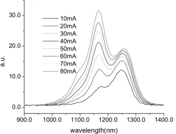
Figure 2 is the measured EL spectrum of the 800µm device. The spectrum has two peaks at 1.25µm and 1.17µm. They correspond to the first quantized state and second quantized state of the QDs. In addition, extra signals can be observed between 1100nm and 1000nm with 240mA and 320mA injection current. This is
considered to be the contribution of energy states in GaAs/InGaAs QWs.
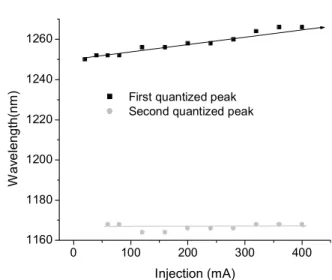
The peak emission power of the 1.25µm peak saturates at 200mA. Its peak position red shifts with increased current. This peak is at 1250nm with 20mA injection. It moves to 1266nm when the injection current is increased to 400mA. The peak emission power of the 1.17µm peak saturates at 320mA. The peak position blue shifts when the current is increased from 60mA to 160mA. It shifts back to 1164nm when the current is increased to 400mA. The emission of GaAs/InGaAs QWs can only be observed with more than 240mA injection. 900 1000 1100 1200 1300 1400 0 2 4 6 8 10 in te ns ity( a. u. ) wavelength(nm) 20mA 40mA 60mA 80mA 120mA 160mA 200mA 240mA 280mA 320mA 360mA 400mA
Fig. 2. The EL spectrum of 800µm device .
0 100 200 300 400 1160 1180 1200 1220 1240 1260 W av e length(nm) Injection (mA) First quantized peak Second quantized peak
The emission spectrum of the 350µm device has the same shape. The peak emission power of the 1.25µm peak saturates at 40mA. Its peak position red shifts with increased current. This peak is at 1248nm with 10mA injection. It moves to 1260nm when the injection current is increased to 80mA. The peak emission power of the 1.17µm peak does not saturate due to lower operation current density. The peak position blue shifts from 1172nm to 1166nm when the current is increased from 20mA to 60mA. It shifts back to 1168nm when the current is increased to 80mA.
Fig. 4. The EL spectrum of 350µm device.
Fig. 5. The current – EL peak curve of 350µm device.
V. DISCUSSION
Several factors influence the emission peaks of the spectrum. In general, with increased injection current, the position of 1.25µm peak red shifts. This can be explained by bandgap narrowing due to increased active layer temperature. The same mechanisms effect should have the effect on the emission of the second quantized state. Thus, the emission peak wavelengths of both quantized states will increase with increasing current. In addition, the magnitude of red shift should approximately be the same because bandgap narrowing will change the positions of quantized states by the same amount.
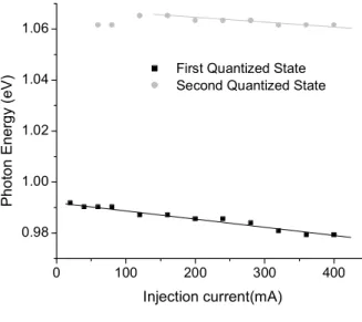
Although, simultaneous red shift of both emission peaks is observed under high current density, 160mA to 400mA for 800µm device and 60mA to 80mA for 350µm device. The decreases of photon energy for both peaks are different. Photon energy of first quantized state decrease more than that of second quantized state, as shown in Fig. 6.
Another effect of increasing injection current is to change the distribution of carriers among different QDs. The origin of this effect is the different carrier capture abilities of QDs with different sizes and the state filling effect. Larger QDs have more chance to capture carriers because they occupy more volume. In addition, the quantized states of larger QDs have lower quantized energy. Thus, carriers tend to populate in larger QDs under equilibrium according to Fermi-Dirac distribution. Under very low injection density, most of the carriers will be captured by larger QDs. As injected current increase, the states of larger QDs are filled up, so more carriers will fall into smaller QDs.
Because the QDs in this sample have a large size variation, inhomogeneous broadening makes the observed emission bandwidth broad. The position of each observed emission peak is affected by both carrier distribution and quantized state position. If carriers tend to distribute at larger QDs, the emission peak will be at the longer wavelength. If carriers tend to distribute at smaller QDs, the emission peak will be at the shorter wavelength. In the observed devices, this effect makes the peak emission position of second quantized states blue shifted as current is increased from 60mA to 160mA for the 800µm device and 10mA to 60mA for the 350µm device. Under higher injection level, this effect is less important because the quantized states of smaller QDs are saturated also. Finally, thermal bandgap narrowing will dominate the direction of emission-peak shift.
The final issue is to explain the different behavior of both emission peaks. It is because the two quantized states have different density distribution. Because the position of quantized level depends on n2. n is 1 for the 900.0 1000.0 1100.0 1200.0 1300.0 1400.0 0.0 10.0 20.0 30.0 a. u. wavelength(nm) 10mA 20mA 30mA 40mA 50mA 60mA 70mA 80mA 0 20 40 60 80 1100 1150 1200 1250 1300 Wa ve le n gt h( n m ) Injection (mA)
First quantized peak Second quantized peak
first quantized state and 2 for the second quantized state. The position of the second quantized level is more sensitive to the dot-size variation than the position of the first quantized level. Thus, the separation between the first and the second quantized levels of a smaller dot will be larger and it will be smaller for a larger dot. If carriers concentrate in larger dots, the separation between two emission peaks will be smaller. If carriers concentrate in smaller dots, the separation between two emission peaks will be larger. For this reason, the directions and amounts of shift of the two emission peaks must be different. The observed separation between the two emission peaks increases as current increases because the increased current will provide more carriers to smaller QDs than to larger QDs.
Fig. 6. The current – photon energy 800µm device.
Fig. 7. The relative position of quantized states in different size QDs.
VI. CONCLUSION
In QD structures, carriers do not distribute uniformly among QDs. Carriers tend to distribute at larger QDs. Combined with state filling effect, it makes the emission
peak of the second quantized state blue shift with increasing current. The nonuniform carrier distribution also leads to the separation of two emission peaks increasing with increased current. On the observed 800µm device, the photon energy difference between the two peaks increases from 70.8meV at 60mA to 78meV at 160mA. By observing the peak separation, the tendency of carrier distribution can be identified.
REFERENCES
[1] Q. Xie, P. Chen, A. Kalburge, T. R. Ramachandran, A. Nayfonov, A. Konkar, and A. Madhukar, “Realization of optically active strained InAs island quantum boxes on GaAs (100) via molecular beam epitaxy and the role of island induced strain fields,” J. Cryst. Growth, vol. 150, p. 357, 1995.
[2] P. M. Varangis, H. Li, G. T. Liu, T. C. Newell, A. Stintz, B. Fuchs, K. J. Malloy, and L. F. Lester, “Low-threshold quantum dot lasers with 201 nm tuning range,” Electron.
Lett., vol. 36, pp. 529–530, 2000.
[3] Bor-Lin Lee, Ching-Fuh Lin, and Jie-Wei Lai, "Experimental evidence of nonuniform carrier distribution in multiple-quantum well laser diodes," IEE Electron. Lett. Vol. 34, pp.1230-1231, 1998.
Large
Small Dot
0 100 200 300 400 0.98 1.00 1.02 1.04 1.06 Phot on Ener gy (e V) Injection current(mA)First Quantized State Second Quantized State