國 立 交 通 大 學
電子工程學系電子研究所碩士班
碩 士 論 文
尖狀氧化鋅奈米柱陣列之製備與場發射特性之
研究
Study on Fabrication and Field Emission
Properties of Sharp ZnO Nanorod Array
研 究 生:顏宏全
尖狀氧化鋅奈米柱陣列之製備與場發射特性之
研究
Study on Fabrication and Field Emission
Properties of Sharp ZnO Nanorod Array
研 究 生 : 顏宏全 Student: Hung-Chuan Yen 指導教授 : 曾俊元 教 授 Advisor: Prof. Tseung-Yuen Tseng
國 立 交 通 大 學
電子工程學系電子研究所碩士班 碩 士 論 文
A Thesis
Submitted to Department of Electronics Engineering & Institute of Electronics
College of Electrical and Computer Engineering National Chiao Tung University
in partial Fulfillment of the Requirements For the Degree of
Master in
Electronics Engineering June 2008
Hsinchu, Taiwan, Republic of China
尖狀氧化鋅奈米柱陣列之製備與場發射特性之
研究
研究生:顏宏全 指導教授:曾俊元
國立交通大學
電子工程學系 電子研究所
摘要
近年來,利用奈米材料當作場發射顯示器的發射源已被
廣泛地研究,其中以低溫製備的氧化鋅奈米柱最受到注意。
但氧化鋅奈米柱本身場發射特性不足以應用於場發射顯示
器上,因此在本論文中,我們藉由濕式與乾式蝕刻的方式,
將柱狀的氧化鋅變成尖狀,以改善其場發射特性。濕式蝕刻
是用稀釋的醋酸去蝕刻未退火與退火過的奈米柱,而乾式蝕
刻是用氬離子轟擊奈米柱。為了更進一步提升其場發射特
性,我們結合濕式與乾式蝕刻的二段蝕刻去形成更尖銳的奈
米柱。經量測結果顯示利用二段蝕刻出的尖狀氧化鋅奈米
柱,具有最佳的場發射特性與穩定性,其可降低兩倍以上的
Study on Fabrication and Field Emission
Properties of Sharp ZnO Nanorod Array
Student: Hung-Chuan Yen Advisor: Tseung-Yuen Tseng
Department of Electronics Engineering & Institute of Electronics National Chiao Tung University
ABSTRACT
In recent years, nanostructures used as emitter sources of field emission display have been researched extensively. ZnO nanorods fabricated by low process temperature attract much attentionspecifically. But they can not be applicable to field emission display due to bad field emission properties themselves. To improve the properties, we use wet and dry etching to sharpen ZnO nanorods in this thesis. For wet etching, we use dilute acetic acid to etch the non-annealed and the annealed nanorods. For dry etching, we use argon ion to bombard nanorods. Also, to improve the properties further, two-step etching combining wet with dry etching is used to form sharper nanorods. From our results, two-step etching exhibits the best field emission properties and stability. It can reduce over twice in the work voltage so that power consumption of field
誌謝
首先誠摯的感謝指導教授曾俊元老師悉心的教導,並提供了這 個資源充分的環境,使我得以一窺電子材料領域的深奧。常常地與 老師討論提供了我正確的研究方向,使我在實驗中獲益匪淺。本論 文的完成特別感謝奕全學長的大力協助,因為有你的意見和分析, 使得實驗的過程中因而順利且完整。 兩年裡的日子,有許多研究室裡共同的實驗生活以及課業上的討 論,讓我特別珍惜這段回憶。感謝群傑、志洋、孟漢、聖裕、岱螢、 明錡、永昇、承佑、冠仲、文仁等學長的指導和費心,啟翔、世偉、 毅函和我共同努力及成長,以及承翰、昱廷、淑炫、盈賢和志文學弟 妹們的陪伴,讓這兩年的研究生活變得絢麗多彩。女朋友韻如在背後 的支持更是我前進的力量,沒有韻如在英文上的指導,生活上的包容 與體諒,相信這兩年不會如此順遂。 最後感謝我的父母,默默地支持和栽培使我能完成這段歷程,這 份喜悅禮是屬於你們的。Contents
Chinese Abstract ... I
English Abstract...II
Acknowledgements... III
Contents ... IV
Table Captions ...VII
Figure Captions... VIII
Chapter 1 Introduction ...1
1.1 Basic Properties of Zinc Oxide ...1
1.2 Field Emission Display ...2
1.3 Synthesis of Zinc Oxide Nanorods ...4
1.3.1 VLS Growth Method ...4
1.3.2 Vapor Solid (VS) Growth Method ...5
1.3.3 Template-Based Synthesis ...5
1.3.4 Hydrothermal Growth Method ...5
1.4 Field Emission Principle ...6
1.5 Sharp Zinc Oxide Nanorods ...8
1.6 Optical Properties of Zinc Oxide ...9
Chapter 2 Experiment Details ...17
2.1 Sample Preparation ...17
2.1.1 Cleaning Wafer...17
2.2 Measurement and Analysis ...19
2.2.1 X-ray Diffraction...19
2.2.2 Four Point Probe ...20
2.2.3 Scanning Electron Microscopy (SEM) ...20
2.2.4 Transmission Electron Microscopy (TEM) ...21
2.2.5 Ultraviolet-Visible Spectrophotometer...21
2.2.6 Cathodoluminescence (CL) ...22
2.2.7 Field Emission Measurement...22
Chapter 3 Results and Discussion ...25
3.1 ZnO Seed Layer ...25
3.1.1 XRD Analysis of Seed Layer...25
3.1.2 SEM Analysis of Seed Layer ...25
3.1.3 Electrical Analysis of Seed Layer...26
3.1.4 Optical Analysis of Seed Layer ...26
3.2 ZnO Nanorod Arrays ...28
3.2.1 SEM Analysis of Nanorod Growth ...28
3.2.1.1 The Influence of Growth Concentration ...28
3.2.1.2 The Influence of Growth Time...28
3.2.2 XRD Analysis of Nanorods ...29
3.2.3 Optical Analysis of Nanorods...29
3.2.4 Field Emission Measurement of Nanorods...30
3.3 Sharp ZnO Nanorod Array ...32
3.3.1 Etching of Non-Annealed Nanorods by Acid...32
3.3.1.1 The SEM Analysis of Morphology ...32
3.3.2 Etching of Annealed Nanorods by Acid ...34
3.3.2.1 The SEM Analysis of Morphology ...34
3.3.2.2 The XRD Analysis of Structure ...35
3.3.2.3 The Optical Analysis...36
3.3.2.4 The Field Emission Measurement...36
3.3.3 Etching of Nanorods by Plasma...37
3.3.3.1 The SEM Analysis of Morphology ...37
3.3.3.2 The TEM Analysis of Structure ...38
3.3.3.3 The XRD Analysis of Structure ...38
3.3.5 Field Emission Property Comparisons of Sharp Nanorods ...41
Chapter 4 Conclusion ...71
References...73
Table Captions
Chapter 1
Table 1-1 Properties of zinc oxide ...11
Chapter 3
Table 3-1 The detail data of field emission properties of ZnO nanorods with different growth concentration...43 Table 3-2 The detail data of field emission properties of ZnO nanorods
with different growth time ...43 Table 3-3 The detail data of field emission properties of annealed ZnO
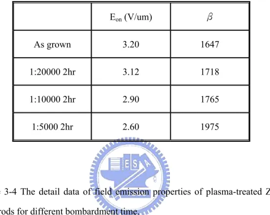
nanorods which are etched with different acidic concentration ...44 Table 3-4 The detail data of field emission properties of plasma-treated
ZnO nanorods for different bombardment time...44 Table 3-5 The detail data of field emission properties of ZnO nanorods
which are sharpened by two-step for different bombardment time...45 Table 3-6 The detail data of field emission properties of sharp ZnO
Figure Captions
Chapter 1
Figure 1-1 Wurtzite structure of ZnO ...12 Figure 1-2 The SEM images of ZnO nanostructure ...12 Figure 1-3 Schematic diagram of (a) CRT structure (b) FED structure ...13 Figure 1-4 Schematic diagram of Spindt-type field emission source ...13 Figure 1-5 Structure of FED with carbon nanotube emitter...14 Figure 1-6 VLS growth mechanism...14 Figure 1-7 Potential energy distribution of emitter surface under electric
field...15 Figure 1-8 SEM images of sharp ZnO nanorods synthesized by different
method (a) One step VS (b) two step VS (c) chemical
solution ...15
Chapter 2
Figure 2-1 Flow chart of experiments ...23 Figure 2-2 The structure of sharpened ZnO nanorods through etching
process ...24 Figure 2-3 Schematic diagram of a high-vacuum chamber system for field emission property measurement...24
Chapter 3
Figure 3-1 The XRD pattern of ZnO seed layer which is annealed at
different temperature ...46 Figure 3-2 The XRD pattern of annealed ZnO seed layers. The seed
layers are deposited under different Ar/O2 flow ratio ...46
Figure 3-3 The SEM images of annealed ZnO seed layer on Si substrate. (a) Top and (b) cross view ...47 Figure 3-4 The optical transmittance of annealed ZnO seed layer...48 Figure 3-5 The pourbaix diagram for zinc...48
2hr, 3hr, and 4hr, respectively. And (b)(d)(f)(h) are
corresponding cross views ...50 Figure 3-8 The XRD patterns of ZnO nanorods which are annealed for
different time ...51 Figure 3-9 The CL spectra of ZnO nanorods which are annealed in
oxygen for different time ...51 Figure 3-10 The bended band diagram of ZnO nanorod (a) before
annealing (b) after annealing in oxygen...52 Figure 3-11 The field emission J-E curves of ZnO nanorods with different growth concentration...52 Figure 3-12 The field emission F-N plots of ZnO nanorods with different
growth concentration...53 Figure 3-13 The field emission J-E curves of ZnO nanorods with different growth time ...53 Figure 3-14 The field emission F-N plots of ZnO nanorods with different
growth time ...54 Figure 3-15 The SEM images of non-annealed nanorods which are etched
with 1:20000 concentrations for different etching time. (a) 5min (b) 15min (c) 1hr (d) 2hr (e) 4hr (f) 5hr...55 Figure 3-16 The etching mechanism of non-annealed nanorods...56 Figure 3-17 The SEM images of non-annealed nanorods which are etched
with different acidic concentration for 2hr. (a) 1:30000 (b) 1:25000 (c) 1:20000 (d) 1:15000 ...56 Figure 3-18 (a)(c)(e) are tilted views of nanorods which are etched with
1:10000 concentration for 1hr, 2hr, and 4hr after short time annealing, respectively. And (b)(d)(f) are corresponding cross views ...57 Figure 3-19 The etching mechanism of annealed nanorods ...58 Figure 3-20 (a)(c)(e) are tilted views of nanorods which are etched with
1:20000, 1:10000, and 1:5000 concentration for 2hr after short time annealing, respectively. And (b)(d)(f) are
corresponding cross views ...59 Figure 3-21 (a)(c)(e) are tilted views of nanorods which are etched for 2hr
with 1:20000, 1:10000, and 1:5000 concentration after long time annealing, respectively. And (b)(d)(f) are corresponding
Figure 3-23 The CL spectra of annealed ZnO nanorods which are etched by acid ...61 Figure 3-24 The field emission J-E curves of annealed ZnO nanorods
which are etched with different acidic concentration ...62 Figure 3-25 The field emission F-N plots of annealed ZnO nanorods
which are etched with different acidic concentration ...62 Figure 3-26 (a)~(e) are the SEM image of plasma-treated nanorods for
bombardment time of 10s, 20s, 30s, 60s, and 120s,
respectively...63 Figure 3-27 The TEM and SAED image of plasma-treated nanorods for
bombardment time of 60s...64 Figure 3-28 The XRD patterns of plasma-treated nanorods which are
bombarded for 120s...65 Figure 3-29 The field emission J-E curves of plasma-treated ZnO
nanorods for different bombardment time ...65 Figure 3-30 The field emission F-N plots of plasma-treated ZnO nanorods for different bombardment time ...66 Figure 3-31 (a)~(e) are the SEM image of nanorods which are sharpened
by two-step etching for bombardment time of 5, 10, 15, 30, 45, 60, and 120s, respectively ...67 Figure 3-32 The field emission J-E curves of ZnO nanorods which are
sharpened by two-step etching for different bombardment time...68 Figure 3-33 The field emission F-N plots of ZnO nanorods which are
sharpened by two-step etching for different bombardment time...68 Figure 3-34 The field emission J-E curves of sharp nanorods by different
methods ...69 Figure 3-35 The field emission F-N plots of sharp nanorods by different
methods ...69 Figure 3-36 The stability measurement of sharp nanorods by different
Chapter 1
Introduction
1.1
Basic Properties of Zinc Oxide
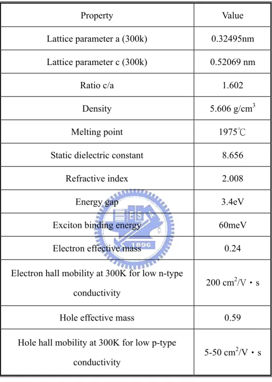
Zinc oxide (ZnO) is a II-VI group semiconductor. It is wurtzite structure as Figure 1-1. The lattice parameter of ZnO wurtzite structure is a = 0.325 nm and c = 0.521 nm. The ratio of c/a which equals to 1.602 is nearly perfect. Its melting point is up to 1975 and thermal stability is ℃ very high. In addition, ZnO materials are generally n-type semiconductors with typical carrier concentration of 1017 cm-3 because of oxygen vacancies or zinc interstitials within them. The properties of ZnO are listed at Table 1-11.
Some important properties of ZnO are as follow: a. Direct wide band gap (3.4eV)
b. Large exciton binding energy (60meV) c. High transparency and conductivity d. Piezoelectricity
e. Bio-safe and biocompatible
For these reasons, ZnO is applicable to ultraviolet light-emitting devices2, ultraviolet laser3, transparent conducting film4, surface acoustic wave (SAW) devices in wireless communication5, and biomedical device6.
In recent years, nanotechnology has been researched extensively. There are many kinds of nanostructures, including zero-dimension (0D) nanostructures such as nanoparticle 7 , nanodot 8 ; one-dimension (1D)
morphology of nanostructures, there are many different properties compared to the bulk. It provides many new applications of electronic and optical devices.
Since the carbon nanotubes (CNTs) were discovered in 1991, one-dimensional semiconductor nanostructures such as nanorods, nanowires, and nanotubes have attracted much attention due to their many unique properties and the possibility. In addition to carbon, other one-dimension materials, like ZnO, GaAs and TiO2, were researched in recent years. Among
them, ZnO nanorods exhibit not only large surface area and high aspect ratio but also many mentioned advantages of ZnO so that they may be used as ultraviolet laser16, field emission display17, gas sensor18, hydrogen storage19, and solar cell20 etc. Figure 1-2 illustrates scanning electron microscopy (SEM) images of several ZnO nanostructures21,22,23,24.
1.2
Field Emission Display
Various kinds of flat panel display devices such as liquid crystal display (LCD), vacuum fluorescent display (VFD), and plasma display panel (PDP), organic light emitting display (OLED) have been developed. Among them, LCD is the most popular flat panel displays. However, there are many drawbacks like low brightness, high cost, high temperature sensitivity, and narrow view angle in LCDs. More and more studies of flat panel display have been investigated lately. FED especially attracts attention in these displays. FED is a vacuum electron device, sharing many common features with the
created by injecting electrons from a cathode onto a phosphor coated screen. In a CRT, the electron source is made up of up to three thermionic cathodes. A set of electromagnetic deflection coils can control electrons to scan the phosphor screen, which is typically held at a potential of 15~30 kV. In a FED, the electron source consists of a matrix-addressed array of millions of cold emitters. This field emission array (FEA) is placed above phosphor faceplate 0.2~2.0um and is aligned such that each phosphor pixel has a dedicated set of field emitters. Thin panel thickness (approximately 2 mm), high image quality, wide view angle (about 170°), quick response (about uS), low power consumption, and high tolerance to environments are all advantages of FED.
Since 1960s, the concepts of FED were demonstrated, and many kinds of cathode emitters have been researched. Spindt successfully fabricated emitters of FED by semiconductor technology, called the Spindt-type cold cathode26. Schematic diagram of Spindt-type cold cathode is showed in Figure1-4. The Spindt-type cold cathode is micro-meter scale emitters with self-aligned metal pyramids and gates. The metal pyramids are usually molybdenum with diameter of 1um. The advantage of Spindt-type cold cathode includes long lifetime, high brightness, and high adequate color purity. However, Spindt-type FED is high cost and its applicable size is not large enough. Other kinds of cathode emitters such as ballistic electron surface emitting device (BSD)27,
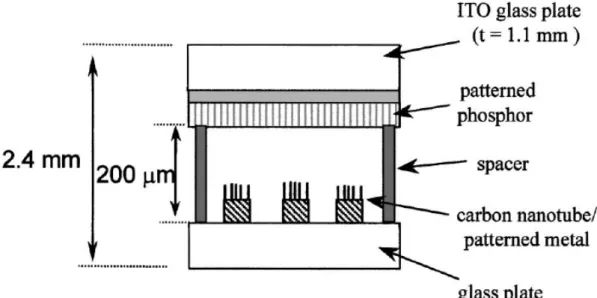
metal insulator metal (MIM)28, surface conduction emitter (SCE)29 and carbon nanotube (CNT) emitter30 have been developed. The CNT emitters have been able to replace the metal pyramids of spindt-type cold cathode recently. The structure of FED with carbon nanotube emitters is showed in Figure1-5.
with CNTs, ZnO nanorods are easy to synthesize large area by low temperature process. Low cost of synthesis and stable chemical property are also the advantage of ZnO nanorods. Therefore, we replace CNTs with ZnO nanorods as cathode emitters in this thesis.
1.3
Synthesis of Zinc Oxide Nanorods
There are a lot of methods to synthesize ZnO nanorods such as vapor-liquid-solid (VLS) method, metal-organic chemical vapor deposition (MOCVD), thermal evaporation, template-based synthesis, and hydrothermal method.
1.3.1
VLS Growth Method
31,32The VLS growth mechanism was originally developed by Wagner and Ellis to produce micrometer-sized whiskers during the 1960s. In a typical VLS growth method, ZnO powder and graphite are mixed appropriately and load into an alumina boat, then the boat is placed in the center of a quartz tube under N2 or Ar flow. As the temperature is increased to the reactive temperature, the
ZnO reacts with graphite to form Zn(g) and CO(g). The gaseous products produced by reactions (1.1) and (1.2) would adsorb and condense on the metal catalytic droplets. Then nucleation is starting and the single crystalline ZnO nanorods grow by the reaction (1.3).The process is showed in Figure1-6.
1.3.2
Vapor Solid (VS) Growth Method
33,34For VS growth methods, such as MOCVD and thermal evaporation, the ZnO nanorods are deposited by chemically gaseous reaction without extra metal catalysts. The gaseous atoms can play the role of the catalyst. In the VS growth mode, control of the nanorod diameter is accomplished by adjusting chamber temperature and vapor pressure. Although VS growth methods can improve the disadvantage of VLS growth methods, the aspect ratio and alignment of ZnO nanorods are worse than VLS.
1.3.3
Template-Based Synthesis
35,36Template-based synthesis uses the porous Anodic Aluminum Oxide (AAO) substrate as the template of the ZnO nanorods. The AAO structure can provide some properties for nanorods, including high pores density, controllable diameter and length of pores, large area and uniform arrays. The holes of the AAOtemplate are filled with ZnO by CVD, sol-gel or hydrothermal method. After filling the ZnO, NaOH solution is used to remove the AAO template. Template-based synthesis is easy and cheap to synthesize ZnO nanorods, but it is not pure enough and hard to create single crystal ZnO nanorods.
1.3.4
Hydrothermal Growth Method
37,38Hydrothermal growth method is the cheapest method to synthesize ZnO nanorods. It has some advantages over other growth methods such as catalyst-free and large area growth, low cost, environmental friendliness, and
The substrate with ZnO seed layer which can help ZnO nanorods grow along C-orientation is put into an aqueous solution of the zinc nitrate hexahydrate ( Zn(NO3)2 . 6H2O (99.9% purity) ) and the
hexamethylenetetramine ( HMT; C6H12N4, (99.9% purity) ) in a vessel. Zinc
nitrate hexahydrate is used as source of zinc and HMT is used to control the PH value. These can be represented by the following reactions:
(CH2)6N4 + 6H2O → 6HCHO + 4NH3 (1.5) NH3 + H2O ↔ NH4+ + OH- (1.6) 2OH- + Zn2+ → Zn(OH)2 (1.7) Zn(OH)2 → ZnO(s)+ H2O (1.8)
Hydrothermal method involves two steps: nucleation and growth. When zinc nitrate hexahydrate and HMT are mixed together, no precipitation accrues initially. With the increase of temperature, the HMT begins to decompose into ammonia and the Zn(OH)2 occurs. Then ZnO nuclei are
formed on the substrate. As soon as the ZnO nuclei are formed, the ZnO nanorods begin to grow. This synthesis of ZnO nanorods without catalysts or templates provides a promising option for the large size production of well-dispersed one-dimensional nanostructure materials.
1.4
Field Emission Principle
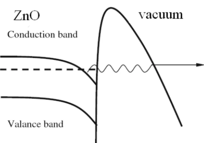
When we applied a negative voltage on nanorods, the negative voltage would induce a strong electric field near the tip of structures. The electric field
electrons to pass through this barrier. This phenomenon of electric tunneling is followed by Fowler-Nordheim tunneling40. The F-N current density can be described by the F-N equation. The F-N equation is as follow41:
3 2 2 2
exp[
]
J
β
β
Α Ε
ΒΦ
=
−
Φ
Ε
(1.9)R
D
S
β
≅
(1.10)Where J is the current density, E is the applied electric field of tip, Φ is the work function (5.37 eV42), β is the field emission enhancement factor, A is 1.5x10⁻¹⁰(AV-2eV), and B is 6.83x10³(eV-3/2V/um). From the equation, we can know that smaller work function generates higher field emission current. That is because the materials with smaller work function exhibits lower barrier height, then electrons can easier tunnel through this barrier. Besides reducing work function, raising β can also generate higher field emission current. The β can be written as Eq. (1.10) where S is dependent on screen effect, D is the distance from anode to cathode, and R is dependent on the radius of electron emitter. If the neighboring emitters are farther, S is larger. It causes higher field emission current. The sharper morphology with smaller R can also contribute to higher current in the equation. To sum up, the field emission current is highly dependent on both the properties of the material and the morphology of the cathode. In this thesis, we would enhance the field emission property by narrowing the radius of cathode emitter top.
3 2
m
β
ΒΦ
= −
(1.12) 2 ln( ) b= Αβ Φ (1.13)A plot of log (J/E2) versus 1/E is a straight line with slop m and intercept b. The value of β can be calculated by the equation (1.12). Besides β, the turn on electric field (Eon) is also considered in field emission measurement. The Eon is
defined as the electric field at the current density of 1.0 μA/cm2. It is a critical electric field differentiating from noise. In this thesis, we judge the field emission of nanorods by β and Eon. Larger β represents sharper tip structure and
lower Eon can reduce the consumption of power.
1.5
Sharp Zinc Oxide Nanorods
It is well known that the sharp ZnO nanorods can improve field emission property. Some researches have demonstrated it by different experiments43,44. To apply ZnO nanorods to FED, we must fabricate sharp nanorods to reduce the power of operation. Many kinds of synthesis of sharp ZnO nanorods have been reported lately such as VS and chemical solution methods. For VS, ZnO nanorods with sharp tip morphologies are fabricated by chemical reaction of gas source. This method can be divided into one step and two step growth. One step growth means that the condition of growth is fixed45, while the condition would be altered during synthesis of nanorods for two step growth46. The
method, sharp nanorods are fabricated by direct oxidation of zinc foil in alkaline zincate ion solution at near room temperature47. The sharp nanorods by chemical solution method are showed in Figure1-8 (c).
VS method is a high temperature process. It is not suitable for application of FED due to low melting point of glass and plastic substrate. While chemical solution method is a process of low temperature, it is restricted by substrate of zinc foil. Therefore, we advance a new process that as-grown ZnO nanorods are etched by acid or plasma to sharpen the nanorods in this thesis.
1.6
Optical Properties of Zinc Oxide
Compared with other direct wide band gap materials, ZnO exhibits a larger exciton binding energy48 which assures more efficient exciton emissions. In addition, its binding energy is also larger than the thermal energy (~26 meV). For those reason, ZnO has attracted considerable attention in optical applications such as ultraviolet light-emitting devices and laser devices. The optical spectrum shows in Figure 1-949.
There are generally two kinds of emission manners in ZnO. One is the ultraviolet emission; the other is the visible emission. The mechanism of the ultraviolet and visible light is shown in Figure1-10. The ultraviolet emission is related to the exciton emission of ZnO. There is an exciton state under the conduction band within ZnO band diagram. An exciting energy would cause electrons to jump to conduction band, and then the electrons might jump to the exciton state. Next, the electrons would spontaneously jump to the valence
Vanheusden et al50, the visible emission originates from the oxygen vacancies. Oxygen vacancies in ZnO can occur in three different charge states: the VΦ state which captures two electrons and is neutral relative to the lattice, the singly ionized VO • state which captured one electron, the VO • • state which do
not trap any electron and is doubly positive charge relative to the lattice. Generally, the VΦ st ate is assumed to be a very shallow donor51. The visible emission, in the main, results from the recombination of the photogenerated hole in the valence band with the singly ionized oxygen vacancy. The more singly ionized oxygen vacancies are, the stronger intensity of visible emission is52.
Table 1-1 Properties of zinc oxide Property Value Lattice parameter a (300k) 0.32495nm Lattice parameter c (300k) 0.52069 nm Ratio c/a 1.602 Density 5.606 g/cm3 Melting point 1975℃
Static dielectric constant 8.656
Refractive index 2.008
Energy gap 3.4eV
Exciton binding energy 60meV Electron effective mass 0.24 Electron hall mobility at 300K for low n-type
conductivity 200 cm
2/V‧s
Hole effective mass 0.59 Hole hall mobility at 300K for low p-type
conductivity 5-50 cm
Figure 1-1 Wurtzite structure of ZnO
Figure 1-3 Schematic diagram of (a) CRT structure (b) FED structure
Figure 1-5 Structure of FED with carbon nanotube emitter
Figure 1-9 Optical spectrum
Chapter 2
Experiment Details
In this chapter, we will introduce the experiment details including sample preparation, measurement and analysis. The flow of experiment is showed in Figure 2-1.
2.1
Sample Preparation
2.1.1
Cleaning Wafer
In the experiment, the p-type Si (100) substrate is cleaned by a standard Radio Corporation of America (RCA) cleaning method and rinsed in acetone for 30 min to remove native oxide and particles from the surface of Si substrate.
2.1.2
Deposition of ZnO Seed Layer
ZnO nanorod array is generally hard to grow on Si substrate due to lattice mismatch. To grow ZnO nanorod array on the substrate, a ZnO seed layer is deposited on Si substrate by radio frequency magnetron sputtering system with 30W for 30 min under 10-2 torr.
2.1.3
Thermal Treatment of ZnO Seed Layer
ZnO seed layer grown by RF sputter is amorphous generally. To improve (002) orientation of ZnO seed layer, a high temperature annealing process is
under O2 flow (35 sccm).
2.1.4
Growth of ZnO Nanorod Array
In this thesis, ZnO nanorod array grows by hydrothermal method. ZnO seed layer on Si substrate is put into an aqueous solution of zinc nitrate hexahydrate (Zn(NO3)2.6H2O (99.9% purity)) and hexamethylenetetramine
( HMT ; C6H12N4, ( 99.9 % purity ) ) in a vessel at 85 for various ℃ growth
times from 1 hr to 4 hr. The concentration of zinc and amine in the mixed solution are varied from 0.0125M to 0.05M.
2.1.5
Fabrication of Sharp Nanorods
There are four methods to sharpen the nanorods in this thesis. They are as following:
a. Etching of non-annealed nanorods by acid b. Etching of annealed nanorods by acid c. Etching of nanorods by plasma
d. Etching of nanorods by combining acid with plasma (two-step etching) For acidic etching, the nanorod array is put in a sealed vessel with dilute acetic acid of 20 mL. The etching temperature is fixed about 85℃. The concentration (Vacid:Vwater) of dilute acetic acid is varied from 1:30000 to
1:5000. And the reactive time is varied from 5min to 5hr. For etching annealed nanorods, the nanorods are annealed by rapid thermal annealing (RTA) at 500℃ for 1min before etching. For plasmatic etching, the substrate covered
varied from 10s to 120s.
To fabricate sharper nanorod array, we combined acidic etching with plasmatic etching. At first, the nanorod arrays without annealing are etched by dilute acetic acid for appropriate time to form raised tips. Then they are etched by plasma to form sharp tips. In this two-step etching, the concentration (Vacetic:Vwater) of dilute acetic acid is fixed in 1:20000, and the etching time is
15min. The etching temperature is kept about 85℃. The bombardment time of plasma is varied from 30s to 120s with 15W under 5x10⁻² torr. Figure 2-2 is the structure of etched nanorod array.
2.2
Measurement and Analysis
2.2.1
X-ray Diffraction
The crystal structure of ZnO nanorod array can be observed by the high resolution X-ray diffractometer (Bede, D1). The X-ray diffraction equipment is often used for identifying the crystal structure. If the angle θ (Bragg`s angle) between the crystal plane and the incident light matches the Bragg`s law (nλ=2dsinθ), the incident light would be diffracted by the crystal plane. And then the reflected x-rays from the respective atomic planes can be measured by the detector. In the Bragg`s law, nλ is an integral number of wavelengths, and d is the distance between two successive crystal planes. The average grain size and orientations can be determined from XRD data. The average grain size of a specimen is estimated from XRD peaks using Scherrer’s formula by
.
.F
C
I
V
Rs
=
⋅
the XRD peak, abbreviated as FWHM, and θ is taken as diffraction angle. The X-ray diffraction measurement with Cu Kα radiation (λ=1.5418 Å ) is operated at 40KV and 40mA. In order to avoid the peak of silicon about 70°, the angle 2θ of the measurement is from 20° to 60°.
2.2.2
Four Point Probe
Four point probe is used to measure the sheet resistance of the sample. The instrument consists of four equally spaced (62.5 mil) tungsten metal tips. During measuring, a supplied current would pass through the outer two probes, and the voltage across the inner two probes is measured. According to the applied current (I) and measured voltage (V), the sheet resistance (Rs) can be derived by the following equation:
(2.2)
The unit of Rs is (Ω/□); C.F. is the correction factor which depends on the sample size and the probe tip spacing. In our measurement, C.F. is
2 ln
π .
2.2.3
Scanning Electron Microscopy (SEM)
Field emission scanning electron Microscopy (FESEM, Hitachi S4700) is used to observe the seed layer surface morphology and film thickness. Besides, it also analyzes the surface structure, morphology, diameter, length and density of ZnO nanostructures. Hitachi S4700 operates at 15 kV under 2x10⁻⁶ torr with the resolution of 1.5 nm. The cold field electron gun is used as the source of
2.2.4
Transmission Electron Microscopy (TEM)
The crystal structure and morphology analysis of ZnO nanorod can be measured by the high resolution transmission electron microscopy (HR-TEM, JEM-2100F). TEM is a microscopy technique whereby a beam of electrons is transmitted through a specimen, interacting with the specimen as it passes through it. An image is formed from the electrons transmitted through the specimen, magnified and focused by an objective lens, and then detected by a sensor such as a CCD camera. And by the selected area electron diffraction (SAED), it can show the crystal structure of ZnO nanorod. The lattice constant of the ZnO nanorod can be observed by HR-TEM.
The sample of TEM is prepared through scratching the nanorods from the substrate, ultrasonic dispersing in ethanol and dripping the solution on a copper grid. The rate of the vibration is about 14000 rpm. The vibration time is 3~5 minutes.
2.2.5
Ultraviolet-Visible Spectrophotometer
The ultraviolet-visible spectrophotometer (Hitachi, U-3010) can be used to analyze UV/VIS spectroscopy of sample. It measures the intensity (I) of light passing through the sample, and compares it to the intensity (I0) of light
before it passes through the sample. The ratio of I/I0 is called the transmittance
(T), and is usually expressed as a percentage. From the transmittance, the band-gap property of material can be understood. The spectrophotometer includes light sources, a holder for the sample, a diffraction grating or
2.2.6
Cathodoluminescence (CL)
The luminescence properties of sample can be measured by the Cathodluminescence (CL, JEOL JSM6500F, Japan) with an electron beam as an excitation source at room temperature. CL is an optical and electrical phenomenon whereby a beam of electrons is generated by an electron gun and then impacts on a material, causing the electrons of atoms to jump from ground state to excited state. Because the excited state is very unstable, the electrons would subsequently jump to ground state. Between the transitions of electrons, the redundant energy would release in the form of heat energy or photon energy. The photon energy is measured by the detector. From the analysis of CL spectrum, the band gap, the defects and impurity of the materials can be understood.
The excited source of CL is 15 KV. The sweeping range is from 350nm to 700nm. The sweeping rate is 2nm per second. The excited depth of electrical beam for ZnO material is several tens nanometer.
2.2.7
Field Emission Measurement
Keithley 237 equipment is used for measuring the current–voltage (I –V) and field emission characteristics. The prepared sample is put in a vacuum chamber under a pressure of 5 × 10⁻⁶ torr at room temperature. A copper electrode probe as an anode with an area of 7.09 × 10⁻³ cm2 is placed above the sample. The measurement equipment is illustrated in Figure 2-3.
Cleaning Wafer
Deposition of ZnO Seed Layer
Thermal Treatment of Seed Layer
Growth of ZnO Nanorod Array by
Hydrothermal Method
Fabrication of Sharp Nanorods
Analysis (XRD,SEM,TEM,CL,FE)
Acidic etching Annealing Plasmatic etching Acidic etching Acidic etching Plasmatic etchingFigure 2-2 The structure of sharpened ZnO nanorods through etching process
Figure 2-3 Schematic diagram of a high-vacuum chamber system for field emission property measurement.
Chapter 3
Results and Discussion
3.1
ZnO Seed Layer
3.1.1
XRD Analysis of Seed Layer
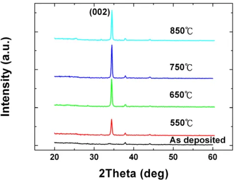
Figure 3-1 shows the XRD patterns of seed layers which are annealed at different temperature under Ar/O2 flow ratio of 3. It indicates that the (002)
orientation of seed layer is improved by annealing. And the (002) peak increases with increase of annealing temperature. But the intensity of (002) peak at 850℃ is weaker than 750℃. It is attributed to the melt of ZnO seed layer at this temperature. Figure 3-2 shows the XRD patterns of seed layers which are deposited under different Ar/O2 flow ratio and annealed at 750℃.
From this figure, it is indicated that the Ar/O2 flow ratio of the strongest (002)
orientation is 3. And the (002) peak decreases with decrease of the ratio. In order to grow nanorod array along C-axis, we choose to deposit seed layer under Ar/O2 flow ratio of 3 and anneal it at 750℃ in this thesis. The FWHM of
this seed layer is 5.62x10⁻³ radian and the diffraction angle is 34.4°. The grain size calculated by Scherrer’s formula (eq. 2.1) is about 30nm.
3.1.2
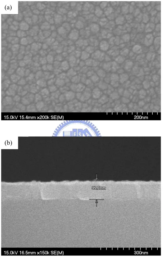
SEM Analysis of Seed Layer
Figure 3-3 is the SEM images of annealed ZnO seed layer, (a) shows the top view and (b) is corresponding cross view. It can be found that there are
fabricate well-aligned ZnO nanorod array.
3.1.3
Electrical Analysis of Seed Layer
The sheet resistance of seed layer can be measured by the four point probe. Many different positions of film are measured for accurate value. The sheet resistance of seed layer before annealing is 104.6(Ω/□) on average. The sheet resistance after annealing is 285.0(Ω/□) on average. It is indicated that the resistance of seed layer increases through annealing in oxygen. It is well-known that resistance of semiconductor is related to carrier concentration and mobility. Higher carrier concentration and mobility can generate higher current. And the mobility of high crystal quality is large than low crystal quality. From the results of XRD, the crystal quality of seed layer would become better after annealing in oxygen. But the resistance not decreases but increase through annealing as above result. It can be explained that the decrease of carrier concentration is more than the increase of mobility. According to some researches, the carriers of ZnO are provided from oxygen vacancy and zinc interstitial53. When the ZnO is annealed in oxygen, the oxygen vacancies would be filled and the structure defects are recovered. Therefore, the carrier concentration would decrease largely so that the sheet resistance increases.
3.1.4
Optical Analysis of Seed Layer
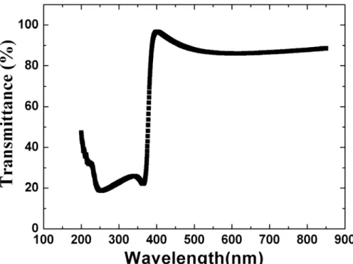
It indicates ZnO exhibits good transmittance for visible light. Therefore, ZnO is applicable to optical device such as solar cell. It also shows a low transmittance region from 250 to 400nm. This is because the energy of light is larger than the band gap of ZnO (3.4eV). When the incident light passes through the sample, the electrons of valence band would absorb the light to jump on higher energy level so that the transmittance decreases.
3.2
ZnO Nanorod Arrays
3.2.1
SEM Analysis of Nanorod Growth
ZnO nanorod array is synthesized by the hydrothermal method. The sources of the hydrothermal method are zinc nitrate hexahydrate and hexamethylenetetramine. It is very important to control the pH value of solution for the hydrothermal method. Figure 3-5 is the pourbaix diagram for zinc. It is indicated that the pH value must be controlled between 6 and 14 for growing nanorod array. If the pH value of the solution is not in this range, there are many other compounds produced, including Zn2+(aq) , Zn(s) and
Zn(OH)42-(aq) .
3.2.1.1 The Influence of Growth Concentration
The solution concentration is a key factor of growing ZnO nanorod arrays by the hydrothermal method. Figure 3-6 is the SEM images of ZnO nanorods with different growth concentration varied from 0.0125 M to 0.05M for same growth time (3 hours) and temperature (85℃). It is observed that the nanorod array is denser with increasing concentration. For the concentration of 0.05M, the ZnO nanorod array is densest. And the array is thinner and inclined for 0.0125M and 0.025M. Besides, the lengths of 0.0125M and 0.05M are shorter on average, and the diameters of 0.025M and 0.05M are thicker.
(85℃). This figure shows that the lengths of nanorods are increased with increasing the growth time, but the length no longer increases after 3hr. It is because the pH value of solution is between 6 and 8 for our growth concentration so that the nanorod growth can happen. During growing, the pH value would decrease gradually. It contributes to stopping growth of nanorods. This figure also shows that the densities and diameters of different growth time are similar. It means that the growth time would not affect the density and diameters of nanorod array.
3.2.2
XRD Analysis of Nanorods
Figure 3-8 shows the XRD patterns of nanorods which are annealed at 500℃ for different time in oxygen environment. It can be observed that the (002) orientation of nanorods is enhanced after annealing. And the (002) peak increases with increase of annealing time. In addition, the FWHM of annealing for 1min and 30 min (both 0.233°) are smaller than as-grown (0.248°). They are indicated that the structure of ZnO nanorod array is improved through annealing process.
3.2.3
Optical Analysis of Nanorods
To understand the source of visible emission in the nanorods, we annealed the ZnO nanorods at 500℃ for different time under oxygen environment. Figure 3-9 is the CL spectra of nanorods with different annealing time. From this figure, it can be found that the UV emission and the visible emission decrease with increasing the time of annealing.
annealing can be understood as follows: ZnO nanostructures are n-type and are generally recognized as exhibiting a depletion layer at their surface. Surface adsorbed oxygen has been proposed as contributing to the formation of this depletion layer, by extracting electrons from the conduction band of ZnO54,55. UV emission arises from the recombination of photogenerated holes and electrons across the band-gap. Band bending at the surface separate the photogenerated electron-hole pairs so that the probability of recombination is reduced. Consequently, the probability of UV emission from the depletion region is much lower than that from the central region of the ZnO crystal56. The depletion would expand after annealing in oxygen due to a decrease of oxygen vacancies within the ZnO. Therefore, the reduced UV emission from the sample annealed in oxygen can be explained by invoking an expanded depletion layer, as show in Figure 3-10.
The decrease of visible emission results from the decrease of the oxygen vacancies. When the nanorods were annealed in oxygen environment, the oxygen atoms would occupy the oxygen vacancies. It leads to the reduction of source of visible emission. So the visible emission would become weak after annealing in oxygen. From this conclusion, it is indicated that the visible emission of ZnO nanorods arises from oxygen vacancies.
3.2.4
Field Emission Measurement of Nanorods
In order to fabricate the ZnO nanorod array which exhibits better field emission characteristic, we should choose a concentration with low density,
The J-E curves of ZnO nanorods with different concentration are showed in Figure 3-11. The corresponding F-N plot is showed in Figure 3-12. It should be noticed that the electrical field value below Eon are not drawn in F-N plot
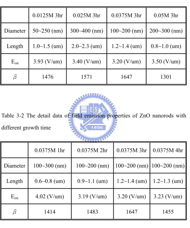
since they are recognized as noise. Field enhance factor (β) can be calculated from the slop of the F-N plot. The details of field emission properties with different concentration are showed in Table 3-1. As shown in this table, the ZnO nanorods which grew in the 0.0125M and 0.05M exhibit the worse field emission properties. For 0.0125M, the nanorod array is inclined due to thinner growth concentration. For 0.05M, the nanorod arrays are so dense that screen effect is serious. And the length of this concentration is shorter than others on average. Therefore, the field emission properties of 0.05M and 0.0125M are worse.
The J-E curves of ZnO nanorods with different growth time are showed in Figure 3-13. The corresponding F-N plot is showed in Figure 3-14. The details of field emission properties with different growth time are showed in Table 3-2. As shown in this table, the ZnO nanorod array which grew for 1hr exhibit worse field emission properties because its length is shorter than others.
Comparing above results, we choose the growth concentration of 0.0375M and growth time of 3hr as growth parameters in this thesis since field emission of the nanorods and the uniform level of nanorod distribution are best.
3.3
Sharp ZnO Nanorod Array
3.3.1
Etching of Non-Annealed Nanorods by Acid
We used acetic acid to etch the nanorods which grew in 0.0375M for 3hr by different acidic concentration (Vacid:Vwater) and etching time. The etching
temperature is fixed at 85℃.
3.3.1.1 The SEM Analysis of Morphology
Figure 3-15 is the SEM images of non-annealed nanorods which are etched with same acidic concentration (1:20000) for different etching time. It is observed that the flat top of as-grown nanorods become raised when they are etched for 5min. About 15min, the raised tops would become more obvious. For 1hr, some of raised tops start to become concave. Most raised tops would become flat or concave tops about 2hr. After 4hr, the six sides of nanorods start to melt together. It results from over etching and too close nanorods. After 5hr, most nanorods are etched too much. It contributes to melt of nanorods.
The etching mechanism of non-annealed nanorods is shown in Figure 3-16. At first, there are many OH- bonded on the top of nanorod. It is proposed that the terminal Zn atom on the polar (0001) surface bonds to three of the underneath O atoms. But it bonds to four O atoms in the ZnO bulk. Therefore, every surface Zn atom exhibits extra charges so that the negative ion (OH-) would adsorb on the positive polar face of (0001) by electrostatic57,58,59. The
energy and is metastable, while the nonpolar faces parallel to the C-axis are the most stable faces and exhibit lower surface energy60. The etching rate of the polar (0001) face is faster than that of the nonpolar faces (the lateral planes). Moreover, it is proposed that more defects were formed near the center of ZnO nanorod61,62. The etching prefers to take place in the metastable (0001) face from the defect-rich initial parts of the ZnO nanorods. Therefore, the center of nanorod would be etched after etching of corners. The concave tops are formed through this etching process. Besides, it is noticed that many hollow nanorods are observed at which nanorods contact. When the nanorod edges contact together, there are dislocations here. The dislocations would generate high energy in the nanorods. It results in etching nanorods easier and deeper. Therefore, the nanorods with contacts are easier to become hollow, while the tops of nanorods without contacts become shallow hole at most.
Figure 3-17 is the SEM images of non-annealed nanorods which are etched for same etching time (2hr) with different acidic concentration. It is observed that the flat top of as-grown nanorods become raised top in weaker acid (1:30000). And some of raised tops would become concave tops in 1:25000. In stronger acid (1:20000 and 1:15000), most raised tops would become flat or concave tops. But the nanorods are etched so much that some of them melt together.
In order to fabricate the ZnO nanorod arrays which exhibit better field emission characteristic, we should choose an etching parameter with sharp tip nanorods. According to above results, a raised top can be fabricated with weaker acidic concentration and shorter etching time. But the weak acidic
1:20000 and 15min as the etching parameters of non-annealed nanorods for improving field emission in this thesis.
3.3.2
Etching of Annealed Nanorods by Acid
The nanorods were annealed in oxygen at 500℃ for improving the crystal quality and reducing defects at first. Then we used acetic acid to etch the nanorods which grew in 0.0375M for 3hr with different etching time and acidic concentration (Vacid:Vwater). And the etching temperature is fixed at 85℃.
3.3.2.1 The SEM Analysis of Morphology
Figure 3-18 is SEM images of nanorods which are etched with same acidic concentration (1:10000) for different etching time. From this figure, it is observed that the flat tops of nanorods become round for short etching time (1hr). And the tops become sharper with increase of etching time. The etching process doesn’t involve with the form of concave tops. The nanorods with sharp tops can be fabricated through this process. It should be noticed that the sharp tops are not perfect structure. There is roughness on the top due to the damage of crystal structure by acid. It would contribute to worse field emission property of nanorods.
From the results of etching of non-annealed and annealed nanorods, it is indicated that the etching mechanisms of them are different. The reason for it is that upon annealing, defects in the crystals would become less and attain thermal equilibrium with a uniform distribution instead of preferentially
still the weakest in the nanorods. So the nanorods are etched isotropicly from the corners into the core. The etching mechanism is shown in Figure 3-19. Figure 3-20 is SEM images of annealed nanorods which are etched with different acidic concentration for same etching time (2hr) after short annealing (1min). It is observed that sharper nanorod tops are fabricated by stronger acid. For weaker acid (1:20000), the corners are etched and the tops of nanorods become round. For stronger acid (1:5000), the top can become needle-like. It would contribute to better field emission property of nanorods. The etching process of different acidic concentration is similar to the results of different etching time mentioned above.
Figure 3-21 is SEM images of annealed nanorods which are etched with different acidic concentration for same etching time (2hr) after longer annealing (30min). Compared to Figure 3-20, it is observed that the nanorods with longer annealing are etched hardly. It results from the stronger crystal structure after longer thermal treatment. The acid is hard to etch them so that these nanorods can’t become as sharp as above nanorods with shorter annealing.
3.3.2.2 The XRD Analysis of Structure
Figure 3-22 shows the XRD patterns of annealed nanorods which are etched with different acidic concentration for same etching time (2hr) after annealing (1min). It can be observed that the (002) orientation of nanorods become weaker after etching. And the (002) peak decreases with increase of acidic concentration. It is indicated that the structure of ZnO nanorod array is
They are like the FWHM of annealed nanorods (0.233°). It is indicated that the average grain sizes are similar even after etching.
3.3.2.3 The Optical Analysis
Figure 3-23 is the CL spectra of annealed nanorods which are etched with the concentration of 1:10000 for 2hr at 85℃. It can be observed that the UV emission increase and visible emission decrease after etching annealed nanorods. The UV emission is affected by surface depletion region and the visible emission is related to oxygen vacancies as above results. When the nanorods are put in dilute acid, the surface region of them would be etched, thus the depletion regions of surface are reduced. And the excited depth of electrical beam for CL is fixed. Therefore, the region which can emit UV light would increase. As a result, UV emission increases after etching process. In addition, the surface defects of nanorods are also reduced due to etching process. It results in the decrease of visible emission.
3.3.2.4 The Field Emission Measurement
The J-E curves of annealed nanorods which are etched with different acidic concentration are showed in Figure 3-24. The corresponding F-N plot is showed in Figure 3-25. The details of field emission properties with different acidic concentration are showed in Table 3-3. As shown in this table, the annealed nanorods which are etched with the concentration of 1:5000 exhibit the best field emission properties. That is because the tops of the nanorods are
results of SEM. The nanorods are destroyed more seriously with increase of etching concentration.
In this thesis, we choose the concentration of 1:5000 and the etching time of 2 hour as our etching parameters of annealed ZnO nanorods for improving field emission property.
3.3.3
Etching of Nanorods by Plasma
Besides acidic etching, nanorods could become sharper through plasmatic etching. We use Ar plasma to etch nanorods which grew in 0.0375M for 3hr with different bombardment time. The RF power is fixed at 15W and the pressure is under 5x10⁻² torr.
3.3.3.1 The SEM Analysis of Morphology
Figure 3-26 shows the SEM images of plasma-treated ZnO nanorod arrays with different bombardment time. For 10s, the edge of nanorod top starts to round due to ion bombardment. About 30s, the nanorods top become cone-like morphology. The cone top is smooth and sharp. The angle of cone top is about 100° for 30s and 60s bombardment. It also can be observed that the nanorods remain perpendicular to the substrate after bombardment. In addition, there is no significant reduction of nanorod length observed until 120s. It indicates that a short plasma exposure would not result in shortening and destruction of nanorods, which would deteriorate the field emission property. After 120s, the nanorods become shorter and rounder. Therefore, we must control the time of bombardment to fabricate sharp ZnO nanorod arrays which exhibit the best
3.3.3.2 The TEM Analysis of Structure
In order to make a detail investigation on structure changes of ZnO nanorods after plasma bombardment, we analyze the nanorods which are etched by Ar plasma for 60s with HRTEM and SAED. Figure 3-27 shows the TEM, HRTEM and SAED images of plasma-treated ZnO nanorod. As shown in this image, the nanorod top is sharp tip as the results of SEM. The inserts of this figure are the HRTEM images of column core and cone top, respectively. These images illustrate that the ZnO wurtzite structure is complete without destruction. It suggests that there is no significant change on the surface crystal structure of plasma-treated nanorod. The other insert of this figure shows the SAED image of cone top. It indicates that the top of plasma-treated nanorod is still single crystal structure. It suggests again that the structure of nanorod is complete. Therefore, the field emission would be deteriorated through plasma bombardment due to complete ZnO nanorod structure. From this SAED image, it also illustrate that the growth direction of ZnO nanorod is along [0001].
3.3.3.3 The XRD Analysis of Structure
Figure 3-28 shows the XRD patterns of plasma-treated ZnO nanorod arrays with bombardment time of 120s. It can be observed that the (002) orientation of nanorods become weaker after etching. In addition, the FWHM of bombarded nanorods is 0.251° larger than as-grown (0.248°). It is indicated that the structure of ZnO nanorod array would be destroyed through ion
3.3.3.4 The Field Emission Measurement
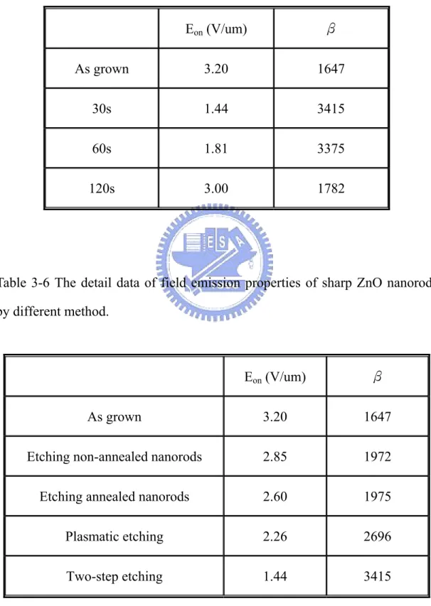
The J-E curves of plasma-treated nanorods with different bombardment time are showed in Figure 3-29. The corresponding F-N plot is showed in Figure 3-30. The details of field emission properties with different bombardment time are showed in Table 3-4. As shown in this table, the nanorods which are bombarded for 60s exhibit the best field emission properties. It is because the tops of nanorods for 60s are sharper than others on the whole.
In this thesis, we choose the bombardment time of 60s as our etching parameters of plasma-treated ZnO nanorods for improving field emission property.
3.3.4
Two-Step Etching
ZnO nanorods have been etched by acid and plasma individually above for small radius of nanorod tip. To improve the field emission further, we combine the acidic etching and plasmatic etching to sharpen nanorod tops. At first, the nanorods are etched by acetic acid to form raised top. Different diameters of raised tops can be fabricated by different concentration and etching time. Then the raised tops are bombarded by Ar ion to form cone tips. Different angles of cone tips can be fabricated by different bombardment time. To fabricate sharper tip, the nanorods which grew in 0.0375M for 3hr at 85℃ are etched with concentration of 1:20000 and etching time of 15min at 85℃. And then they are etched for different bombardment time with 15W under
3.3.4.1 The SEM Analysis of Morphology
Figure 3-31 is the SEM images of nanorods which are etched by two-step etching with different bombardment time. After acidic etching, the nanorod top is divided into two parts called raised top and remaining rod. For 5s, the raised top and remaining rod are still like as-etched top. When bombardment time is 10s, the raised tops become cone tips and the top edge of remaining rod is pared off. Up to 30s, the nanorod tops become sharp tip. The angle of tip is about 70° smaller than the angle with only plasmatic etching. It contributes to further improvement of field emission property. From 30s to 60s, the angles of nanorod tips are similar. About 120s, the nanorods become shorter and rounder. It is like the plasmatic etching nanorods at 120s. It means that field emission property of nanorods would be deteriorated through long bombardment time. Therefore, we must control the time of bombardment to fabricate the sharpest ZnO nanorod arrays which exhibit the best field emission property.
The reason that the nanorods with two-step etching are sharper than only plasmatic etching is as follows: the acidic etching can narrow the diameter of top to form raised top at first. The following ion bombardment would sharpen this raised top further. Since the diameter of raised top is smaller than as-grown nanorod tops, two-step etching tops would be sharper than plasmatic etching.
3.3.4.2 The Field Emission Measurement
the nanorods which are bombarded for 30s exhibit the best field emission properties. It is because the tops of nanorods for 30s are sharper than others on the whole.
In this thesis, we choose 30s as our bombardment time in two-step etching for improving field emission property.
3.3.5
Field Emission Property Comparisons of
Sharp Nanorods
To apply ZnO nanorod array to field emission display, the turn-on electrical field (Eon) should be small and field enhancement factor (β) should be
large. For this reason, we try four methods to sharpen ZnO nanorods. First, non-annealed nanorods are etched with a weaker acid (1:20000) for 15min at 85℃. Second, nanorods are annealed initially at 500℃ for 1min. Then they are etched with a stronger acid (1:5000) for 1hr at 85℃. Third, nanorods are etched by Ar plasma with 15W for 60s under 5x10⁻² torr. Fourth, nanorods are etched initially in a weaker acid (1:20000) at 85℃ for 15min as first method. Then they are etched by Ar plasma with 15W for 30s under 5x10⁻² torr. The J-E curves of sharpened ZnO nanorods by different methods are showed in Figure 3-34. The corresponding F-N plot is showed in Figure 3-35. The details of field emission properties with different methods are showed in Table 3-6. It shows that the field emission property of nanorods with raised top is better than as-grown. It is attributed to narrowing the radius of top. It also can be observed
destroying the structure. Compared to two-step etching, the angles of cone tops of plasma-treated nanorods are larger. It results in worse field emission property than two-step etching. Although the tops of annealed nanorods which are etched by acid are very sharp in these methods, the structures of them would be destroyed due to acidic etching. It contributes to even worse property than plasmatic etching.
Besides Eon and β, the stability of ZnO nanorod array is important to
practical application of field emission display. To study the stability of nanorod arrays, the field emission property is measured through one thousand cycles. And then the Eon values are extracted. Figure 3-36 is the Eon variations of
as-grown, plasmatic etching, and two-step etching. From this figure, it is observed that the Eon of two-step etching is the most stable. It is because a
nanorod with plat top generates current from different position every time. And a nanorod with sharp top generates current at its apex every time. Therefore, the stability of two-step etching with the sharpest top is the best. Form above results, it is indicated that the two-step etching exhibits not only the best field emission properties but also the best stability.
Table 3-1 The detail data of field emission properties of ZnO nanorods with different growth concentration
0.0125M 3hr 0.025M 3hr 0.0375M 3hr 0.05M 3hr Diameter 50~250 (nm) 300~400 (nm) 100~200 (nm) 200~300 (nm)
Length 1.0~1.5 (um) 2.0~2.3 (um) 1.2~1.4 (um) 0.8~1.0 (um) Eon 3.93 (V/um) 3.40 (V/um) 3.20 (V/um) 3.50 (V/um)
β 1476 1571 1647 1301
Table 3-2 The detail data of field emission properties of ZnO nanorods with different growth time
0.0375M 1hr 0.0375M 2hr 0.0375M 3hr 0.0375M 4hr Diameter 100~300 (nm) 100~200 (nm) 100~200 (nm) 100~200 (nm)
Length 0.6~0.8 (um) 0.9~1.1 (um) 1.2~1.4 (um) 1.2~1.3 (um) Eon 4.02 (V/um) 3.19 (V/um) 3.20 (V/um) 3.23 (V/um)
Table 3-3 The detail data of field emission properties of annealed ZnO nanorods which are etched with different acidic concentration
Eon (V/um) β
As grown 3.20 1647
1:20000 2hr 3.12 1718
1:10000 2hr 2.90 1765
1:5000 2hr 2.60 1975
Table 3-4 The detail data of field emission properties of plasma-treated ZnO nanorods for different bombardment time.
Eon (V/um) β
As grown 3.20 1647
30s 2.51 2546 60s 2.26 2696 120s 3.07 1614
Table 3-5 The detail data of field emission properties of ZnO nanorods which are sharpened by two-step for different bombardment time.
Eon (V/um) β
As grown 3.20 1647
30s 1.44 3415 60s 1.81 3375 120s 3.00 1782
Table 3-6 The detail data of field emission properties of sharp ZnO nanorods by different method.
Eon (V/um) β
As grown 3.20 1647
Etching non-annealed nanorods 2.85 1972 Etching annealed nanorods 2.60 1975 Plasmatic etching 2.26 2696
Figure 3-1 The XRD patterns of ZnO seed layer which is annealed at different temperature.
Figure 3-3 The SEM images of annealed ZnO seed layer on Si substrate. (a) Top and (b) cross view
(a)
(a) (b)
(c) (d)
(e) (f)
(a) (b)
(c) (d)
(e) (f)
Figure 3-8 The XRD patterns of ZnO nanorods which are annealed for different time
Figure 3-10 The bended band diagram of ZnO nanorod (a) before annealing (b) after annealing in oxygen
Ec EF Ec Ev Ev boundary depletion (a) (b)
Figure 3-12 The field emission F-N plots of ZnO nanorods with different growth concentration
Figure 3-14 The field emission F-N plots of ZnO nanorods with different growth time
Figure 3-15 The SEM images of non-annealed nanorods which are etched with 1:20000 concentrations for different etching time. (a) 5min (b) 15min (c) 1hr (d) 2hr (e) 4hr (f) 5hr.
(a)
(e) (f)
(c) (d)
Figure 3-16 The etching mechanism of non-annealed nanorods
Figure 3-17 The SEM images of non-annealed nanorods which are etched with
(a) (b) (c) (d) Defect OH- OH- OH- OH- OH-OH-
Figure 3-18 (a)(c)(e) are tilted views of nanorods which are etched with 1:10000 concentration for 1hr, 2hr, and 4hr after short time annealing, respectively. And (b)(d)(f) are corresponding cross views.
(a) (b)
(c) (d)
Figure 3-19 The etching mechanism of annealed nanorods Defect Etching Annealing Etching OH- OH- OH- OH-
Figure 3-20 (a)(c)(e) are tilted views of nanorods which are etched with 1:20000, 1:10000, and 1:5000 concentration for 2hr after short time annealing, respectively. And (b)(d)(f) are corresponding cross views.
(a) (b)
(c) (d)
Figure 3-21 (a)(c)(e) are tilted views of nanorods which are etched for 2hr with 1:20000, 1:10000, and 1:5000 concentration after long time annealing, respectively. And (b)(d)(f) are corresponding cross views.
(a)
(c) (d)
Figure 3-22 The XRD patterns of annealed nanorods which are etched with different acidic concentration
Figure 3-24 The field emission J-E curves of annealed ZnO nanorods which are etched with different acidic concentration
Figure 3-26 (a)~(e) are the SEM image of plasma-treated nanorods for bombardment time of 10s, 20s, 30s, 60s, and 120s, respectively.
(a) (b)
(c) (d)
Figure 3-27 The TEM and SAED image of plasma-treated nanorods for bombardment time of 60s.
Figure 3-28 The XRD patterns of plasma-treated nanorods which are bombarded for 120s
Figure 3-30 The field emission F-N plots of plasma-treated ZnO nanorods for different bombardment time
(a) (b) (c) (e) (d) (f) (g)
Figure 3-32 The field emission J-E curves of ZnO nanorods which are sharpened by two-step etching for different bombardment time
Figure 3-34 The field emission J-E curves of sharp nanorods by different methods